Table of Contents
Advertisement
Quick Links
Advertisement
Table of Contents

Related Manuals for IEI Technology WAFER-AL


Summary of Contents for IEI Technology WAFER-AL
- Page 1 WAFER-AL SBC WAFER-AL CPU Card MODEL: WAFER-AL ® ® ® 3.5” SBC with 14nm Intel Pentium /Celeron On-board SoC, DP++, VGA, LVDS, Dual PCIe GbE, USB 3.0, PCIe Mini, mSATA, SATA 6Gb/s, RS-232/422/485, HD Audio, SIM Slot and RoHS User Manual Page I Rev.
- Page 2 WAFER-AL SBC Revision Date Version Changes May 3, 2018 1.01 Deleted E series SKUs Updated Chapter 6: Software Drivers November 30, 2017 1.00 Initial release Page II...
- Page 3 WAFER-AL SBC Copyright COPYRIGHT NOTICE The information in this document is subject to change without prior notice in order to improve reliability, design and function and does not represent a commitment on the part of the manufacturer. In no event will the manufacturer be liable for direct, indirect, special, incidental, or consequential damages arising out of the use or inability to use the product or documentation, even if advised of the possibility of such damages.
- Page 4 WAFER-AL SBC Manual Conventions WARNING Warnings appear where overlooked details may cause damage to the equipment or result in personal injury. Warnings should be taken seriously. CAUTION Cautionary messages should be heeded to help reduce the chance of losing data or damaging the product.
-
Page 5: Table Of Contents
PTIONAL TEMS 3 CONNECTORS ......................14 3.1 P ..............15 ERIPHERAL NTERFACE ONNECTORS 3.1.1 WAFER-AL Layout ................... 15 3.1.2 Peripheral Interface Connectors ..............16 3.1.3 External Interface Panel Connectors ............... 17 3.2 I ..............18 NTERNAL ERIPHERAL ONNECTORS 3.2.1 +12V DC-IN Power Connector ............... 18 3.2.2 Audio Connector .................... - Page 6 WAFER-AL SBC 3.2.11 PCIe Mini Card Slot ..................29 3.2.12 Power and HDD LED Connector ..............31 3.2.13 Power Button Connector ................32 3.2.14 Reset Button Connector ................. 33 3.2.15 RS-232 Serial Port Connectors ..............34 3.2.16 RS-232/422/485 Serial Port Connectors ............35 3.2.17 SATA 6Gb/s Connectors .................
- Page 7 WAFER-AL SBC 4.8 C .................... 63 HASSIS NSTALLATION 4.8.1 Airflow ......................63 4.8.2 Motherboard Installation ................. 63 4.9 I ............63 NTERNAL ERIPHERAL EVICE ONNECTIONS 4.9.1 Audio Kit Installation ..................63 4.9.2 AT Power Connection ..................64 4.9.3 SATA Drive Connection ................... 66 5 BIOS ..........................
- Page 8 WAFER-AL SBC 5.4.1 North Bridge Configuration ................92 5.4.1.1 Intel IGD Configuration ................92 5.4.2 South Bridge Configuration ................94 5.4.2.1 HD-Audio Configuration ................96 5.4.2.2 PCI Express Configuration ............... 97 5.4.2.2.1 Onboard LAN ..................98 5.4.2.2.2 MINI-PCIE ..................99 5.4.2.3 SATA Configuration ................
- Page 9 WAFER-AL SBC List of Figures Figure 1-1: WAFER-AL ........................2 Figure 1-2: Connectors (Front Side) ..................... 4 Figure 1-3: Connectors (Solder Side) ................... 5 Figure 1-4: Dimensions with Heatsink (mm) ................6 Figure 1-5: Data Flow Diagram ...................... 7 Figure 3-1: Connector and Jumper Locations (Front Side) ............. 15 Figure 3-2: Connector and Jumper Locations (Solder Side) ...........
- Page 10 WAFER-AL SBC Figure 3-27: HDMI Connector Pinout Locations ................ 43 Figure 3-28: LAN Connector ......................44 Figure 3-29: USB 3.0 Port Pinout Locations ................45 Figure 3-30: VGA Connector ....................... 46 Figure 4-1: SO-DIMM Installation ....................50 Figure 4-2: Removing the Retention Screw ................51 Figure 4-3: Inserting the Full-size mSATA Module into the Slot at an Angle ......
- Page 11 WAFER-AL SBC List of Tables Table 1-1: WAFER-AL Model Variations ..................3 Table 1-2: Technical Specifications ....................9 Table 3-1: Peripheral Interface Connectors ................17 Table 3-2: Rear Panel Connectors ....................17 Table 3-3: +12V DC-IN Power Connector Pinouts ..............18 Table 3-4: Audio Connector Pinouts ..................
- Page 12 WAFER-AL SBC Table 4-1: AT/ATX Mode Select Switch Settings ............... 57 Table 4-2: LVDS Voltage Select Jumper Settings ..............59 Table 4-3: LVDS Backlight Mode Select Jumper Settings............60 Table 4-4: LVDS Panel Resolution Selection ................61 Table 4-5: RS-232/422/485 Mode Selection ................62 Table 5-1: BIOS Navigation Keys ....................
- Page 13 WAFER-AL SBC List of BIOS Menus BIOS Menu 1: Main ........................71 BIOS Menu 2: Advanced ......................72 BIOS Menu 3: Trusted Computing ....................73 BIOS Menu 4: ACPI Settings ....................... 74 BIOS Menu 5: F81866 Super IO Configuration ................75 BIOS Menu 6: Serial Port n Configuration .................
-
Page 15: Introduction
WAFER-AL SBC Chapter Introduction Page 1... -
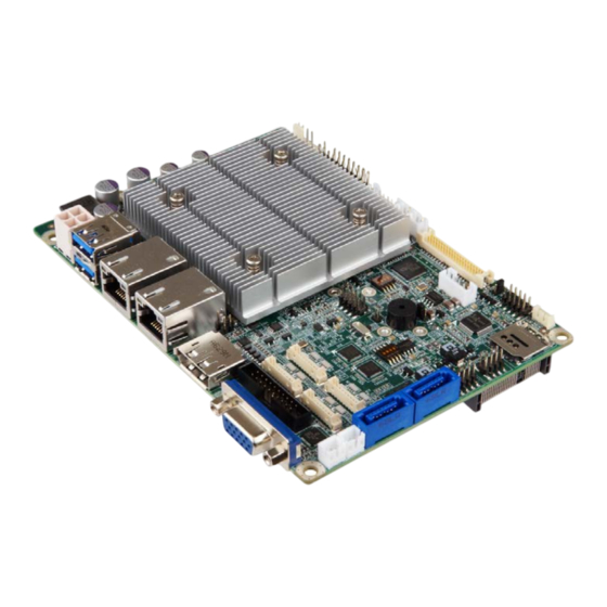
Page 16: Introduction
WAFER-AL SBC 1.1 Introduction Figure 1-1: WAFER-AL ® The WAFER-AL series is a 3.5” single bard computer. It has an on-board 14nm Intel ® ® Pentium or Celeron processor, and supports one 204-pin 1867/1600 MHz single-channel DDR3 Low Voltage (DDR3L) SDRAM SO-DIMM slot with up to 8.0 GB of memory. -
Page 17: Model Variations
WAFER-AL SBC 1.2 Model Variations The model variations of the WAFER-AL series are listed below. Model No. Display Interface ® ® Intel Pentium N4200 on-board SoC DP++, LVDS, VGA WAFER-AL-N2 (up to 2.5 GHz, quad-core, TDP=6 W) ® ® Intel... -
Page 18: Connectors
WAFER-AL SBC 1.4 Connectors The connectors on the WAFER-AL are shown in the figure below. Figure 1-2: Connectors (Front Side) Page 4... -
Page 19: Figure 1-3: Connectors (Solder Side)
WAFER-AL SBC Figure 1-3: Connectors (Solder Side) Page 5... -
Page 20: Dimensions
WAFER-AL SBC 1.5 Dimensions The dimensions of the WAFER-AL series are listed in Figure 1-4. Figure 1-4: Dimensions with Heatsink (mm) Page 6... -
Page 21: Data Flow
WAFER-AL SBC 1.6 Data Flow Figure 1-5 shows the data flow between the system chipset, the CPU and other components installed on the motherboard. Figure 1-5: Data Flow Diagram Page 7... -
Page 22: Technical Specifications
WAFER-AL SBC 1.7 Technical Specifications WAFER-AL technical specifications are listed below. Specification WAFER-AL ® ® Intel Pentium N4200 on-board SoC (up to 2.5 GHz, quad-core, 2 MB cache, TDP=6 W) ® ® Intel Celeron N3350 on-board SoC (up to 2.4 GHz, dual-core, 2 MB cache, TDP=6 W) -
Page 23: Table 1-2: Technical Specifications
WAFER-AL SBC Specification WAFER-AL USB Ports 2 x USB 3.0 on rear I/O 4 x USB 2.0 by 8-pin (2x4) header Front Panel 1 x Power LED & HDD LED by 6-pin (1x6) wafer 1 x Power button by 2-pin wafer... -
Page 24: Unpacking
WAFER-AL SBC Chapter Unpacking Page 10... -
Page 25: Anti-Static Precautions
Only handle the edges of the PCB: Don't touch the surface of the motherboard. Hold the motherboard by the edges when handling. 2.2 Unpacking Precautions When the WAFER-AL is unpacked, please do the following: Follow the antistatic guidelines above. -
Page 26: Packing List
If any of the components listed in the checklist below are missing, do not proceed with the installation. Contact the IEI reseller or vendor the WAFER-AL was purchased from or contact an IEI sales representative directly by sending an email to sales@ieiworld.com. -
Page 27: Optional Items
WAFER-AL SBC 2.4 Optional Items The following are optional components which may be separately purchased: Item and Part Number Image RS-232/422/485 cable, 250 mm, p=1.25 (P/N : 32005-003500-200-RS) Dual USB port cable, 210mm, p=2.0 mm (P/N: 32001-008600-200-RS) Audio cable, 300mm, p=2.0 mm (P/N: 32007-005200-200-RS) Infineon TPM 2.0 module, 20-pin, firmware v5.5... -
Page 28: Connectors
WAFER-AL SBC Chapter Connectors Page 14... -
Page 29: Peripheral Interface Connectors
WAFER-AL SBC 3.1 Peripheral Interface Connectors This chapter details all the jumpers and connectors. 3.1.1 WAFER-AL Layout The figures below show all the connectors and jumpers. Figure 3-1: Connector and Jumper Locations (Front Side) Figure 3-2: Connector and Jumper Locations (Solder Side) -
Page 30: Peripheral Interface Connectors
WAFER-AL SBC 3.1.2 Peripheral Interface Connectors The table below lists all the connectors on the board. Connector Type Label +12V DC-IN power connector 4-pin Molex PWR1 Audio connector 10-pin header AUDIO1 Battery connector 2-pin wafer Digital I/O connector 10-pin header... -
Page 31: External Interface Panel Connectors
WAFER-AL SBC SIM card slot Micro SIM card slot SIM1 SMBus/I C connector 4-pin wafer J_SMB1 SPI Flash Connector 6-pin wafer J_SPI1 TPM connector 20-pin header TPM1 USB 2.0 connector 8-pin header USB1, USB2 EC firmware update connector 2-pin header... -
Page 32: Internal Peripheral Connectors
WAFER-AL SBC 3.2 Internal Peripheral Connectors The section describes all of the connectors on the WAFER-AL. 3.2.1 +12V DC-IN Power Connector CN Label: PWR1 4-pin Molex, p=4.2 mm CN Type: CN Location: See Figure 3-3 CN Pinouts: See Table 3-3 The connector supports the +12V power supply. -
Page 33: Audio Connector
WAFER-AL SBC 3.2.2 Audio Connector CN Label: AUDIO1 CN Type: 10-pin header, p=2.00 mm CN Location: See Figure 3-4 CN Pinouts: See Table 3-4 The audio connector is connected to external audio devices including speakers and microphones for the input and output of audio signals to and from the system. -
Page 34: Battery Connector
Dispose of used batteries according to instructions and local regulations. NOTE: It is recommended to attach the RTC battery onto the system chassis in which the WAFER-AL is installed. CN Label: CN Type: 2-pin wafer, p=1.25 mm CN Location:... -
Page 35: Digital I/O Connector
WAFER-AL SBC Description VBAT+ Table 3-5: Battery Connector Pinouts 3.2.4 Digital I/O Connector CN Label: DIO1 CN Type: 10-pin header, p=2.00 mm CN Location: See Figure 3-6 See Table 3-6 CN Pinouts: The 8-bit digital I/O connector provides programmable input and output for external devices. -
Page 36: Fan Connector
WAFER-AL SBC 3.2.5 Fan Connector CN Label: CPU_FAN1 4-pin wafer, p=2.54 mm CN Type: CN Location: See Figure 3-7 CN Pinouts: See Table 3-7 The fan connector attaches to a cooling fan. Figure 3-7: Fan Connector Location Description +V12S Rotation Signal... -
Page 37: Idp Connector (Optional)
WAFER-AL SBC 3.2.6 iDP Connector (Optional) CN Label: 20-pin box header, p=2.00 mm CN Type: CN Location: See Figure 3-8 CN Pinouts: See Table 3-8 The internal DisplayPort (iDP) connector supports HDMI, LVDS, VGA, DVI and DisplayPort devices with up to 2560x1600 resolution. The iDP connector is only available in iDP SKUs. -
Page 38: Lvds Backlight Inverter Connector
WAFER-AL SBC 3.2.7 LVDS Backlight Inverter Connector CN Label: INV1 5-pin wafer, p=2.00 mm CN Type: CN Location: See Figure 3-9 CN Pinouts: See Table 3-9 The backlight inverter connector provides power to an LCD panel. Figure 3-9: Backlight Inverter Connector Location... -
Page 39: Lvds Lcd Connector
WAFER-AL SBC 3.2.8 LVDS LCD Connector CN Label: LVDS1 40-pin crimp, p=1.25 mm CN Type: CN Location: See Figure 3-10 CN Pinouts: See Table 3-10 The LVDS connector is for an LCD panel connected to the board. The voltage provided to the monitor connected to the LVDS connector is set to 3.3 V by default. -
Page 40: Lan Led Connectors
WAFER-AL SBC Description Description LVDS_B_TX1-N LVDS_B_TX2-N LVDS_B_TX1-P LVDS_B_TX2-P GROUND GROUND LVDS_B_TXCLK-N LVDS_B_TX3-N LVDS_B_TXCLK-P LVDS_B_TX3-P GROUND GROUND GROUND GROUND +LCD VCC +LCD VCC +LCD VCC +LCD VCC +LCD VCC +LCD VCC Table 3-10: LVDS Connector Pinouts 3.2.9 LAN LED Connectors CN Label:... -
Page 41: Msata Module Slot
WAFER-AL SBC Description +3.3V LAN1_LED_LINK#_ACT Table 3-11: LAN1 LED Connector (JLAN_LED1) Pinouts Description +3.3V LAN2_LED_LINK#_ACT Table 3-12: LAN2 LED Connector (JLAN_LED2) Pinouts 3.2.10 mSATA Module Slot CAUTION: If an mSATA module is installed in the mSATA slot (MINI-PCIE1), the SATA port 2 (SATA2) will be disabled. Choose either the SATA2 connector or the mSATA module for storage. -
Page 42: Figure 3-12: Msata Module Slot Location
WAFER-AL SBC Figure 3-12: mSATA Module Slot Location Description Description PCIE_WAKE# VCC3 1.5V PCIE_CLK# PCIE_CLK PCIRST# PCIE_RXN (SATA_RX+) PCIE_RXP (SATA_RX-) 1.5V SMBCLK PCIE_TXN (SATA_TX-) SMBDATA PCIE_TXP (SATA_TX+) USBD- USBD+ VCC3 VCC3 1.5V Page 28... -
Page 43: Pcie Mini Card Slot
WAFER-AL SBC Description Description VCC3 Table 3-13: mSATA Module Slot Pinouts 3.2.11 PCIe Mini Card Slot CN Label: MINI-PCIE2 CN Type: Half-size/Full-size PCIe Mini card slot CN Location: See Figure 3-13 CN Pinouts: See Table 3-14 The PCIe Mini card slot is for installing a PCIe Mini expansion card with USB interface, such as 3G modules. -
Page 44: Table 3-14: Pcie Mini Card Slot Pinouts
WAFER-AL SBC Description Description PCIRST# PCIE_RXN PCIE_RXP 1.5V SMBCLK PCIE_TXN SMBDATA PCIE_TXP USBD- USBD+ VCC3 VCC3 1.5V VCC3 Table 3-14: PCIe Mini Card Slot Pinouts Page 30... -
Page 45: Power And Hdd Led Connector
WAFER-AL SBC 3.2.12 Power and HDD LED Connector CN Label: 6-pin wafer, p=2.00 mm CN Type: CN Location: See Figure 3-14 CN Pinouts: See Table 3-15 The CN1 connector connects to power and HDD LED indicators. Figure 3-14: Power and HDD LED Connector Location... -
Page 46: Power Button Connector
WAFER-AL SBC 3.2.13 Power Button Connector CN Label: PWR_BTN1 CN Type: 2-pin wafer, p=2.00 mm CN Location: See Figure 3-15 CN Pinouts: See Table 3-16 The power button connector connects to a power button. Figure 3-15: Power Button Connector Location... -
Page 47: Reset Button Connector
WAFER-AL SBC 3.2.14 Reset Button Connector CN Label: RST_BTN1 CN Type: 2-pin wafer, p=2.00 mm CN Location: See Figure 3-16 CN Pinouts: See Table 3-17 The reset button connector connects to a reset button. Figure 3-16: Reset Button Connector Location... -
Page 48: Serial Port Connectors
WAFER-AL SBC 3.2.15 RS-232 Serial Port Connectors CN Label: COM3, COM4 9-pin wafer, p=1.25 mm CN Type: CN Location: See Figure 3-17 CN Pinouts: See Table 3-18 The serial connectors provide RS-232 connection. Figure 3-17: RS-232 Serial Port Connector Locations PIN NO. -
Page 49: Rs-232/422/485 Serial Port Connectors
WAFER-AL SBC 3.2.16 RS-232/422/485 Serial Port Connectors CN Label: COM1, COM2 9-pin wafer, p=1.25 mm CN Type: CN Location: See Figure 3-18 CN Pinouts: See Table 3-19 These two connectors provide RS-232, RS-422 or RS-485 communications. The default mode is set to RS-232 by the on-board switch. To configure the connectors as RS-422 or RS-485, please refer to Section 4.7.6. -
Page 50: Sata 6Gb/S Connectors
WAFER-AL SBC PIN NO. RS-232 RS-422 RS-485 TXD422- TXD485- TXD422+ TXD485+ RXD422+ RXD422- Table 3-20: RS-232/422/485 Cable Pinouts 3.2.17 SATA 6Gb/s Connectors CN Label: SATA1, SATA2 CN Type: 7-pin SATA connector CN Location: See Figure 3-19 The SATA 6Gb/s connector is connected to a SATA 6Gb/s device. The SATA 6Gb/s device transfers data at speeds as high as 6Gb/s. -
Page 51: Sata Power Connectors
WAFER-AL SBC CAUTION: If an mSATA module is installed in the mSATA slot (MINI-PCIE1), the SATA port 2 (SATA2) will be disabled. Choose either the SATA2 connector or the mSATA module for storage. 3.2.18 SATA Power Connectors CN Label: SATA_PWR1, SATA_PWR2 2-pin wafer, p=2.00 mm... -
Page 52: Sim Card Slot
WAFER-AL SBC 3.2.19 SIM Card Slot CN Label: SIM1 Micro SIM card slot CN Type: CN Location: See Figure 3-21 The SIM card slot accepts a micro SIM card for network communication. Figure 3-21: SIM Card Slot Location 3.2.20 SMBus/I... -
Page 53: Spi Flash Connector
WAFER-AL SBC Description SMBus (I C) DATA SMBus (I C) CLK Table 3-22: SMBus/I C Connector Pinouts 3.2.21 SPI Flash Connector CN Label: J_SPI1 CN Type: 6-pin wafer, p=1.25 mm CN Location: See Figure 3-23 CN Pinouts: See Table 3-23 The 6-pin SPI Flash connector is used to flash the BIOS. -
Page 54: Tpm Connector
WAFER-AL SBC 3.2.22 TPM Connector CN Label: TPM1 CN Type: 20-pin header, p=2.54 mm CN Location: See Figure 3-24 CN Pinouts: See Table 3-24 The Trusted Platform Module (TPM) connector secures the system on bootup. Figure 3-24: TPM Connector Location... -
Page 55: Usb 2.0 Connectors
WAFER-AL SBC 3.2.23 USB 2.0 Connectors CN Label: USB1, USB2 CN Type: 8-pin header, p=2.00 mm CN Location: See Figure 3-25 CN Pinouts: See Table 3-25 These USB connectors provide four USB 2.0 ports by dual-port USB cable. Figure 3-25: USB Connector Locations PIN NO. -
Page 56: External Peripheral Interface Connector Panel
WAFER-AL SBC 3.3 External Peripheral Interface Connector Panel Figure 3-26 shows the WAFER-AL external peripheral interface connector (EPIC) panel. The EPIC panel consists of the following: 1 x DisplayPort++ connector 2 x GbE LAN connector 2 x USB 3.0 connector ... -
Page 57: Figure 3-27: Hdmi Connector Pinout Locations
WAFER-AL SBC HDMI DisplayPort TMDS DATA2+ TMDS DATA2- TMDS DATA1+ TMDS DATA1- TMDS DATA0+ TMDS DATA0- TMDS CLK+ TMDS CLK- DP_HDMI_SEL DP_HDMI_SEL AUXP AUXN HDMI HPD DP HPD HDMI PWR DP PWR Table 3-26: HDMI Connector Pinouts Figure 3-27: HDMI Connector Pinout Locations... -
Page 58: Lan Connectors
See Figure 3-26 See Table 3-28 CN Pinouts: The WAFER-AL has two external USB 3.0 ports. The USB connector can be connected to a USB 2.0 or USB 3.0 device. The pinouts of USB 3.0 connectors are shown below. Page 44... -
Page 59: Vga Connector
WAFER-AL SBC Description Description USB_VCC USB_VCC USB2_D0- USB2_D0- USB2_D0+ USB2P0_D0+ USB3P0_RXDN1 USB3P0_RXDN2 USB3P0_RXDP1 USB3P0_RXDP2 USB3P0_TXDN1 USB3P0_TXDN2 USB3P0_TXDP1 USB3P0_TXDP2 Table 3-28: USB 3.0 Port Pinouts Figure 3-29: USB 3.0 Port Pinout Locations 3.3.4 VGA Connector CN Label: VGA1 CN Type: 15-pin Female... -
Page 60: Figure 3-30: Vga Connector
WAFER-AL SBC Figure 3-30: VGA Connector Description Description GREEN BLUE VCC / NC DDC DAT HSYNC VSYNC DDCCLK Table 3-29: VGA Connector Pinouts Page 46... -
Page 61: Installation
WAFER-AL SBC Chapter Installation Page 47... -
Page 62: Anti-Static Precautions
Electrostatic discharge (ESD) can cause serious damage to electronic components, including the WAFER-AL. Dry climates are especially susceptible to ESD. It is therefore critical that whenever the WAFER-AL or any other electrical component is handled, the following anti-static precautions are strictly adhered to. - Page 63 Turn all power to the WAFER-AL off: When working with the WAFER-AL, make sure that it is disconnected from all power supplies and that no electricity is being fed into the system. Before and during the installation of the WAFER-AL DO NOT: ...
-
Page 64: So-Dimm Installation
WAFER-AL SBC 4.3 SO-DIMM Installation To install an SO-DIMM, please follow the steps below and refer to Figure 4-1. Figure 4-1: SO-DIMM Installation Step 1: Locate the SO-DIMM socket. Place the board on an anti-static mat. Step 2: Align the SO-DIMM with the socket. Align the notch on the memory with the notch on the memory socket. -
Page 65: Full-Size Msata Module Installation
WAFER-AL SBC 4.4.1 Full-size mSATA Module Installation To install a full-size mSATA module, please follow the steps below. Step 1: Locate the PCIe Mini slot (MINI-PCIE1). See Chapter 3. Step 2: Remove the retention screw as shown in Figure 4-2. -
Page 66: Half-Size Msata Module Installation
WAFER-AL SBC Step 4: Secure the mSATA module with the retention screw previously removed (Figure 4-4). Step 0: Figure 4-4: Securing the mSATA Module 4.4.2 Half-size mSATA Module Installation To install a half-size mSATA module, please follow the steps below. -
Page 67: Figure 4-5: Removing The Retention Screw And The Standoff
WAFER-AL SBC Figure 4-5: Removing the Retention Screw and the Standoff Step 3: Install the previously removed standoff to the screw hole for the half-size mSATA module (Figure 4-6). Figure 4-6: Installing the Standoff Step 4: Line up the notch on the card with the notch on the slot. Slide the mSATA module into the slot at an angle of about 20º... -
Page 68: Figure 4-7: Inserting The Half-Size Msata Module Into The Slot At An Angle
WAFER-AL SBC Figure 4-7: Inserting the Half-size mSATA Module into the Slot at an Angle Step 5: Secure the half-size mSATA module with the retention screw previously removed (Figure 4-8). Step 0: Figure 4-8: Securing the Half-size mSATA Module Page 54... -
Page 69: Pcie Mini Card Installation
WAFER-AL SBC 4.5 PCIe Mini Card Installation The PCIe Mini card slot (MINI-PCIE2) allows installation of either a full-size or half-size PCIe Mini card. To install a full-size PCIe Mini card, please refer to the steps described in Section 4.4 above. -
Page 70: Figure 4-10: Sim Card Installation
WAFER-AL SBC Step 3: Open the slot cover and place a SIM card onto the slot. The cut mark on the corner should be facing away from the slot as shown in Figure 4-10. Figure 4-10: SIM Card Installation Step 4: Close the slot cover and lock it by sliding it in the direction as shown by the arrow in Figure 4-11. -
Page 71: System Configuration
WAFER-AL SBC 4.7 System Configuration The system configuration is controlled by buttons, jumpers and switches. The system configuration should be performed before installation. 4.7.1 AT/ATX Mode Select Switch CN Label: J_ATX_AT1 CN Type: Switch CN Location: See Figure 4-12 CN Settings: See Table 4-1 The AT/ATX mode select switch specifies the systems power mode as AT or ATX. -
Page 72: Clear Cmos Button
CN Location: See Figure 4-13 If the WAFER-AL fails to boot due to improper BIOS settings, use the button to clear the CMOS data and reset the system BIOS information. To clear the CMOS, disconnect the battery (BT1) and press the clear CMOS button for about 3 seconds. -
Page 73: Lvds Voltage Select Jumper
4.7.3 LVDS Voltage Select Jumper WARNING: Permanent damage to the screen and WAFER-AL may occur if the wrong voltage is selected with this jumper. Please refer to the user guide that came with the monitor to select the correct voltage. -
Page 74: Lvds Backlight Mode Select Jumper
WAFER-AL SBC 4.7.4 LVDS Backlight Mode Select Jumper Jumper Label: BL_MODE1 3-pin header, p=2.00 mm Jumper Type: Jumper Settings: See Table 4-3 Jumper Location: See Figure 4-15 The LVDS backlight mode selection jumper allows setting the mode of the LVDS backlight. -
Page 75: Lvds Panel Resolution Select Switch
WAFER-AL SBC 4.7.5 LVDS Panel Resolution Select Switch Jumper Label: DIP switch Jumper Type: Jumper Settings: See Table 4-4 Jumper Location: See Figure 4-16 The SW1 selects the resolution of the LCD panel connected to the LVDS connector. * ON=0, OFF=1; Single=S, Dual=D... -
Page 76: Rs-232/422/485 Mode Select Switch
WAFER-AL SBC 4.7.6 RS-232/422/485 Mode Select Switch Jumper Label: DIP switch Jumper Type: Jumper Settings: See Table 4-5 Jumper Location: See Figure 4-17 The SW2 selects RS-232/422/485 mode of the COM1 and COM2 serial ports. SW2 (1) SW2 (2) Description... -
Page 77: Chassis Installation
The chassis should have fans and vents as necessary to keep things cool. The WAFER-AL must be installed in a chassis with ventilation holes on the sides allowing airflow to travel through the heat sink surface. In a system with an individual power supply unit, the cooling fan of a power supply can also help generate airflow through the board surface. -
Page 78: At Power Connection
0: 4.9.2 AT Power Connection Follow the instructions below to connect the WAFER-AL to an AT power supply. WARNING: Disconnect the power supply power cord from its AC power source to prevent a sudden power surge to the WAFER-AL. -
Page 79: Figure 4-19: Power Cable To Motherboard Connection
WAFER-AL SBC Step 2: Connect the Power Cable to the Motherboard. Connect the 4-pin (2x2) Molex type power cable connector to the AT power connector on the motherboard. See Figure 4-19. Figure 4-19: Power Cable to Motherboard Connection Step 3: Connect Power Cable to Power Supply. -
Page 80: Sata Drive Connection
WAFER-AL SBC 4.9.3 SATA Drive Connection The WAFER-AL is shipped with two SATA cables. To connect the SATA drive to the connector, please follow the steps below. Step 1: Locate the SATA connector and the SATA power connector. The locations of the connectors are shown in Chapter 3. -
Page 81: Figure 4-21: Sata Drive Cable Connection
WAFER-AL SBC Figure 4-21: SATA Drive Cable Connection Step 3: Connect the cable to the SATA disk. Connect the connector on the other end of the cable to the connector at the back of the SATA drive. See Figure 4-21. -
Page 82: Bios
WAFER-AL SBC Chapter BIOS Page 68... -
Page 83: Introduction
WAFER-AL SBC 5.1 Introduction The BIOS is programmed onto the BIOS chip. The BIOS setup program allows changes to certain system settings. This chapter outlines the options that can be changed. NOTE: Some of the BIOS options may vary throughout the life cycle of the product and are subject to change without prior notice. -
Page 84: Getting Help
WAFER-AL SBC Function Decrease the numeric value or make changes F1 key General help, only for Status Page Setup Menu and Option Page Setup Menu F2 key Load previous values. F3 key Load optimized defaults F4 key Save changes and Exit BIOS Esc key Main Menu –... -
Page 85: Main
WAFER-AL SBC The following sections completely describe the configuration options found in the menu items at the top of the BIOS screen and listed above. 5.2 Main The Main BIOS menu (BIOS Menu 1) appears when the BIOS Setup program is entered. -
Page 86: Advanced
WAFER-AL SBC System Time [xx:xx:xx] Use the System Time option to set the system time. Manually enter the hours, minutes and seconds. 5.3 Advanced Use the Advanced menu (BIOS Menu 2) to configure the CPU and peripheral devices through the following sub-menus:... -
Page 87: Trusted Computing
WAFER-AL SBC 5.3.1 Trusted Computing Use the Trusted Computing menu (BIOS Menu 3) to configure settings related to the Trusted Computing Group (TCG) Trusted Platform Module (TPM). Aptio Setup Utility – Copyright (C) 2017 American Megatrends, Inc. Advanced Configuration Enables or Disables BIOS... -
Page 88: Acpi Settings
WAFER-AL SBC 5.3.2 ACPI Settings The ACPI Settings menu (BIOS Menu 4) configures the Advanced Configuration and Power Interface (ACPI) options. Aptio Setup Utility – Copyright (C) 2017 American Megatrends, Inc. Advanced ACPI Settings ACPI Sleep State [S3 (Suspend to RAM] ---------------------- : Select Screen... -
Page 89: F81866 Super Io Configuration
WAFER-AL SBC 5.3.3 F81866 Super IO Configuration Use the F81866 Super IO Configuration menu (BIOS Menu 5) to set or change the configurations for the serial ports. Aptio Setup Utility – Copyright (C) 2017 American Megatrends, Inc. Advanced F81866 Super IO Configuration... -
Page 90: Serial Port 1 Configuration
WAFER-AL SBC 5.3.3.1.1 Serial Port 1 Configuration Serial Port [Enabled] Use the Serial Port option to enable or disable the serial port. Disabled Disable the serial port Enable the serial port Enabled EFAULT Change Settings [IO=3F8h; IRQ=4] Use the Change Settings option to change the serial port IO port address and interrupt address. -
Page 91: Serial Port 2 Configuration
WAFER-AL SBC 5.3.3.1.2 Serial Port 2 Configuration Serial Port [Enabled] Use the Serial Port option to enable or disable the serial port. Disabled Disable the serial port Enable the serial port Enabled EFAULT Change Settings [IO=2F8h; IRQ=3] Use the Change Settings option to change the serial port IO port address and interrupt address. -
Page 92: Serial Port 3 Configuration
WAFER-AL SBC 5.3.3.1.3 Serial Port 3 Configuration Serial Port [Enabled] Use the Serial Port option to enable or disable the serial port. Disabled Disable the serial port Enable the serial port Enabled EFAULT Change Settings [IO=3E8h; IRQ=10] Use the Change Settings option to change the serial port IO port address and interrupt address. -
Page 93: Serial Port 4 Configuration
WAFER-AL SBC 5.3.3.1.4 Serial Port 4 Configuration Serial Port [Enabled] Use the Serial Port option to enable or disable the serial port. Disabled Disable the serial port Enable the serial port Enabled EFAULT Change Settings [IO=2E8h; IRQ=10] Use the Change Settings option to change the serial port IO port address and interrupt address. -
Page 94: F81866 H/W Monitor
WAFER-AL SBC 5.3.4 F81866 H/W Monitor The F81866 H/W Monitor menu (BIOS Menu 7) contains the fan configuration submenus and displays operating temperature, fan speeds and system voltages. Aptio Setup Utility – Copyright (C) 2017 American Megatrends, Inc. Advanced PC Health Status Smart Fan Mode Select >... -
Page 95: Smart Fan Mode Configuration
WAFER-AL SBC +3.3VSB 5.3.4.1 Smart Fan Mode Configuration Use the Smart Fan Mode Configuration submenu (BIOS Menu 8) to configure fan temperature and speed settings. Aptio Setup Utility – Copyright (C) 2017 American Megatrends, Inc. Advanced Smart Fan Mode Configuration... -
Page 96: Usb Configuration
WAFER-AL SBC CPU Temperature 2 If CPU temperature is higher than the value set in this BIOS option, the fan duty cycle is 85. Use the + or – key to change the value or enter a decimal number between 1 and 100. - Page 97 WAFER-AL SBC USB Devices The USB Devices Enabled field lists the USB devices that are enabled on the system Legacy USB Support [Enabled] Use the Legacy USB Support BIOS option to enable USB mouse and USB keyboard support. Normally if this option is not enabled, any attached USB mouse or USB keyboard does not become available until a USB compatible operating system is fully booted with all USB drivers loaded.
-
Page 98: Cpu Configuration
WAFER-AL SBC 5.3.6 CPU Configuration Use the CPU Configuration menu (BIOS Menu 10) to view detailed CPU specifications and configure the CPU. Aptio Setup Utility – Copyright (C) 2017 American Megatrends, Inc. Advanced CPU Configuration Enable/Disable Intel SpeedStep Intel(R) Celeron(R) CPU N3350 @ 1.10GHz... - Page 99 WAFER-AL SBC Enabled Enables the C-state Intel Virtualization Technology [Disabled] Use the Intel Virtualization Technology option to enable or disable virtualization on the ® system. When combined with third party software, Intel Virtualization technology allows several OSs to run on the same system at the same time.
-
Page 100: Rtc Wake Settings
WAFER-AL SBC 5.3.7 RTC Wake Settings The RTC Wake Settings menu (BIOS Menu 11) configures RTC wake event. Aptio Setup Utility – Copyright (C) 2017 American Megatrends, Inc. Advanced Wake system with Fixed Time [Disabled] Enable or disable System wake on alarm event. When... -
Page 101: Power Saving Configuration
WAFER-AL SBC Wake up second After setting the alarm, the computer turns itself on from a suspend state when the alarm goes off. 5.3.8 Power Saving Configuration Use the Power Saving Configuration menu (BIOS Menu 12) to configure system to reduce power consumption in system off state. -
Page 102: Serial Port Console Redirection
WAFER-AL SBC 5.3.9 Serial Port Console Redirection The Serial Port Console Redirection menu (BIOS Menu 13) allows the console redirection options to be configured. Console redirection allows users to maintain a system remotely by re-directing keyboard input and text output through the serial port. -
Page 103: Legacy Console Redirection Settings
WAFER-AL SBC 5.3.9.1 Legacy Console Redirection Settings The Legacy Console Redirection Settings menu (BIOS Menu 14) allows the legacy console redirection options to be configured. Aptio Setup Utility – Copyright (C) 2017 American Megatrends, Inc. Advanced Select a COM port to... -
Page 104: Iei Feature
WAFER-AL SBC 5.3.10 IEI Feature Use the IEI Feature menu (BIOS Menu 15) to configure One Key Recovery function. Aptio Setup Utility – Copyright (C) 2017 American Megatrends, Inc. Advanced iEi Feature Auto Recovery Function Reboot and recover Auto Recovery Function... -
Page 105: Chipset
WAFER-AL SBC 5.4 Chipset Use the Chipset menu (BIOS Menu 16) to access the north bridge and south bridge configuration menus WARNING! Setting the wrong values for the Chipset BIOS selections in the Chipset BIOS menu may cause the system to malfunction. -
Page 106: North Bridge Configuration
WAFER-AL SBC 5.4.1 North Bridge Configuration Use the North Bridge Configuration menu (BIOS Menu 17) to configure the Intel IGD settings. Aptio Setup Utility – Copyright (C) 2017 American Megatrends, Inc. Chipset > Intel IGD Configuration Intel IGD Configuration Memory Information --------------------- : Select Screen... -
Page 107: Bios Menu 18: Intel Igd Configuration
WAFER-AL SBC Aptio Setup Utility – Copyright (C) 2017 American Megatrends, Inc. Chipset IGD Configuration Select which of IGD/PCI Primary Display [IGD] Graphics device should Integrated Graphics Device [Enable] be Primary Display. DVMT Pre-Allocated [256M] DVMT Total Gfx Mem [MAX] --------------------- : Select Screen... -
Page 108: South Bridge Configuration
WAFER-AL SBC then only be used as graphics memory, and is no longer available to applications or the operating system. Configuration options are listed below: 128M 256M EFAULT 512M DVMT Total Gfx Mem [MAX] Use the DVMT Total Gfx Mem option to select DVMT5.0 total graphic memory size used by the internal graphic device. -
Page 109: Bios Menu 19: South Bridge Configuration
WAFER-AL SBC Aptio Setup Utility – Copyright (C) 2017 American Megatrends, Inc. Chipset Auto Power Button Function [Disable (ATX)] Select the state system > HD-Audio Configuration should be when restoring > PCI Express Configuration on AC Power Loss. > SATA Configuration... -
Page 110: Hd-Audio Configuration
WAFER-AL SBC 5.4.2.1 HD-Audio Configuration Use the HD-Audio Configuration menu (BIOS Menu 20) to configure the HD Audio. Aptio Setup Utility – Copyright (C) 2017 American Megatrends, Inc. Chipset HD-Audio Configuration Enable/Disable HD-Audio HD-Audio Support [Enable] Support --------------------- : Select Screen ↑... -
Page 111: Pci Express Configuration
WAFER-AL SBC 5.4.2.2 PCI Express Configuration Use the PCI Express Configuration menu (BIOS Menu 21) to configure the PCI Express. Aptio Setup Utility – Copyright (C) 2017 American Megatrends, Inc. Chipset PCI Express Configuration Control the PCI Express > Onboard LAN1 Root Port. -
Page 112: Onboard Lan
WAFER-AL SBC 5.4.2.2.1 Onboard LAN Use the Onboard LAN menus (BIOS Menu 22) to configure the LAN 1 or LAN 2 port. Aptio Setup Utility – Copyright (C) 2017 American Megatrends, Inc. Chipset Onboard LAN1 [Enable] Control the PCI Express Root Port. -
Page 113: Mini-Pcie
WAFER-AL SBC 5.4.2.2.2 MINI-PCIE Use the MINI-PCIE menus (BIOS Menu 23) to configure the PCIe Mini slots. Aptio Setup Utility – Copyright (C) 2017 American Megatrends, Inc. Chipset MINI-PCIE1 [Enable] Control the PCI Express PCIe Speed [Auto] Root Port. Enable: Enable PCIe root... -
Page 114: Sata Configuration
WAFER-AL SBC 5.4.2.3 SATA Configuration SATA Configuration menu (BIOS Menu 24BIOS Menu 24BIOS Menu 24BIOS Menu 24BIOS Menu 24) to change and/or set the configuration of the SATA devices installed in the system. BIOS Menu 24BIOS Menu 24 Aptio Setup Utility – Copyright (C) 2017 American Megatrends, Inc. -
Page 115: Security
WAFER-AL SBC Hot Plug [Disabled] Use the Hot Plug option to enable or disable the SATA device hot plug. Disables the SATA device hot plug. Disabled EFAULT Enables the SATA device hot plug Enabled 5.5 Security Use the Security menu (BIOS Menu 25) to set system and user passwords. -
Page 116: Boot
WAFER-AL SBC 5.6 Boot Use the Boot menu (BIOS Menu 26) to configure system boot options. Aptio Setup Utility – Copyright (C) 2017 American Megatrends, Inc. Main Advanced Chipset Security Boot Save & Exit Boot Configuration Select the keyboard Bootup NumLock State... - Page 117 WAFER-AL SBC Quiet Boot [Enabled] Use the Quiet Boot BIOS option to select the screen display when the system boots. Normal POST messages displayed Disabled OEM Logo displayed instead of POST messages Enabled EFAULT Launch PXE OpROM [Disabled] Use the Launch PXE OpROM option to enable or disable boot option for legacy network devices.
-
Page 118: Bios Menu 27: Save & Exit
WAFER-AL SBC 5.7 Save & Exit Use the Save & Exit menu (BIOS Menu 27) to load default BIOS values, optimal failsafe values and to save configuration changes. Aptio Setup Utility – Copyright (C) 2017 American Megatrends, Inc. Main Advanced... - Page 119 WAFER-AL SBC Save as User Defaults Use the Save as User Defaults option to save the changes done so far as user defaults. Restore User Defaults Use the Restore User Defaults option to restore the user defaults to all the setup options.
-
Page 120: Software Drivers
WAFER-AL SBC Chapter Software Drivers Page 106... -
Page 121: Available Drivers
WAFER-AL SBC 6.1 Available Drivers All the drivers for the WAFER-AL are available on IEI Resource Download Center (https://download.ieiworld.com). Type WAFER-AL and press Enter to find all the relevant software, utilities, and documentation. Figure 6-1: IEI Resource Download Center IEI provides the following drivers for Windows 7, Windows 8 and Windows 10 operating systems. -
Page 122: Driver Download
6.2 Driver Download To download drivers from IEI Resource Download Center, follow the steps below. Step 1: Go to https://download.ieiworld.com. Type WAFER-AL and press Enter. Step 2: All product-related software, utilities, and documentation will be listed. You can choose Driver to filter the result. - Page 123 WAFER-AL SBC NOTE: To install software from the downloaded ISO image file in Windows 8, 8.1 or 10, double-click the ISO file to mount it as a virtual drive to view its content. On Windows 7 system, an additional tool (such as Virtual CD-ROM Control Panel from Microsoft) is needed to mount the file.
-
Page 124: A Regulatory Compliance
WAFER-AL SBC Appendix Regulatory Compliance Page 110... - Page 125 WAFER-AL SBC DECLARATION OF CONFORMITY This equipment has been tested and found to comply with specifications for CE marking. If the user modifies and/or installs other devices in the equipment, the CE conformity declaration may no longer apply. FCC WARNING This equipment complies with Part 15 of the FCC Rules.
-
Page 126: B Product Disposal
WAFER-AL SBC Appendix Product Disposal Page 112... - Page 127 WAFER-AL SBC CAUTION: Risk of explosion if battery is replaced by an incorrect type. Only certified engineers should replace the on-board battery. Dispose of used batteries according to instructions and local regulations. Outside the European Union–If you wish to dispose of used electrical and electronic products outside the European Union, please contact your local authority so as to comply with the correct disposal method.
-
Page 128: C Bios Menu Options
WAFER-AL SBC Appendix BIOS Menu Options Page 114... - Page 129 WAFER-AL SBC System Date [xx/xx/xx] ......................71 System Time [xx:xx:xx] ....................... 72 Security Device Support [Disable] ..................73 ACPI Sleep State [S3 (Suspend to RAM)] ................74 Serial Port [Enabled] ......................76 Change Settings [IO=3F8h; IRQ=4] ..................76 Transfer Mode [RS232] ......................76 Serial Port [Enabled] ......................
- Page 130 WAFER-AL SBC DVMT Pre-Allocated [256MB] ....................93 DVMT Total Gfx Mem [MAX] ....................94 Primary IGFX Boot Display [Auto] ..................94 Restore on AC Power Loss [Last State] ................95 HD-Audio Support [Enable] ....................96 Onboard LAN1/2 [Enable] ....................98 MINI-PCIE1/ MINI-PCIE2 [Enable] ..................
-
Page 131: D Digital I/O Interface
WAFER-AL SBC Appendix Digital I/O Interface Page 117... - Page 132 WAFER-AL SBC The DIO connector on the WAFER-AL is interfaced to GPIO ports on the Super I/O chipset. The DIO has both 8-bit digital inputs and 8-bit digital outputs. The digital inputs and digital outputs are generally control signals that control the on/off circuit of external devices or TTL devices.
- Page 133 WAFER-AL SBC AH – 6FH Sub-function: AL – 9 :Set the digital port as OUTPUT :Digital I/O output value Assembly Language Sample 2 AX, 6F09H ;setting the digital port as output BL, 09H ;digital value is 09H Digital Output is 1001b...
-
Page 134: E Watchdog Timer
WAFER-AL SBC Appendix Watchdog Timer Page 120... - Page 135 WAFER-AL SBC NOTE: The following discussion applies to DOS. Contact IEI support or visit the IEI website for drivers for other operating systems. The Watchdog Timer is a hardware-based timer that attempts to restart the system when it stops working. The system may stop working because of external EMI or software bugs.
- Page 136 WAFER-AL SBC NOTE: The Watchdog Timer is activated through software. The software application that activates the Watchdog Timer must also deactivate it when closed. If the Watchdog Timer is not deactivated, the system will automatically restart after the Timer has finished its countdown.
-
Page 137: F Hazardous Materials Disclosure
WAFER-AL SBC Appendix Hazardous Materials Disclosure Page 123... - Page 138 WAFER-AL SBC The details provided in this appendix are to ensure that the product is compliant with the Peoples Republic of China (China) RoHS standards. The table below acknowledges the presences of small quantities of certain materials in the product, and is applicable to China RoHS only.
- Page 139 WAFER-AL SBC 此附件旨在确保本产品符合中国 RoHS 标准。以下表格标示此产品中某有毒物质的含量符 合中国 RoHS 标准规定的限量要求。 本产品上会附有”环境友好使用期限”的标签,此期限是估算这些物质”不会有泄漏或突变”的 年限。本产品可能包含有较短的环境友好使用期限的可替换元件,像是电池或灯管,这些元 件将会单独标示出来。 部件名称 有毒有害物质或元素 铅 汞 镉 六价铬 多溴联苯 多溴二苯 醚 (Pb) (Hg) (Cd) (CR(VI)) (PBB) (PBDE) 壳体 显示 印刷电路板 金属螺帽 电缆组装 风扇组装 电力供应组装 电池 O: 表示该有毒有害物质在该部件所有物质材料中的含量均在 SJ/T 11363-2006 (现由 GB/T 26572-2011 取代) 标准规定的限量要求以下。...
Need help?
Do you have a question about the WAFER-AL and is the answer not in the manual?
Questions and answers