Table of Contents
Advertisement
Quick Links
SERVICE MANUAL
Ver. 1.0 2004. 12
AUDIO POWER SPECIFICATIONS (US MODEL)
POWER OUTPUT AND TOTAL HARMONIC DISTORTION
60 watts per channel minimum continuous average power into
4 ohms, both channels driven from 20 Hz to 20 kHz with no more
than 0.08% total harmonic distortion per Car Audio Ad Hoc
Committee standards.
Other Specifications
Circuit system
OTL (output transformerless) circuit
Pulse power supply
Inputs
RCA pin jacks
High level input connector
Outputs
Speaker terminals
Suitable speaker impedance
2 – 8 Ω (stereo)
4 – 8 Ω (when used as a bridging amplifier)
Maximum outputs
Four speakers:
120 W × 4 (at 4 Ω)
150 W × 4 (at 2 Ω)
Three speakers:
120 W × 2 + 300 W × 1 (at 4 Ω)
Rated outputs (supply voltage at 14.4 V)
Four speakers:
60 W RMS × 4 (20 Hz – 20 kHz,
0.08% THD + N, at 4 Ω)
75 W RMS × 4 (20 Hz – 20 kHz,
0.1% THD + N, at 2 Ω)
Three speakers:
60 W RMS × 2 + 150 W RMS × 1 (20
Hz – 20 kHz, 0.1% THD + N, at 4 Ω)
SN Ratio
97 dBA (Reference 1W into 4 Ω)
Frequency response
5 Hz – 50 kHz (
Harmonic distortion
0.005% or less (at 1 kHz)
Sony Corporation
9-879-366-01
2004L04-1
e Vehicle Company
© 2004. 12
Published by Sony Engineering Corporation
SPECIFICATIONS
+0
dB)
–3
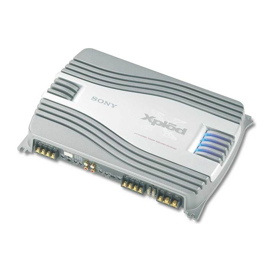
XM-SD46X
Input level adjustment range
0.3 – 6.0 V (RCA pin jacks)
1.2 – 12 V (High level input)
High-pass filter
50 – 300 Hz, –12 dB/oct
Low-pass filter
50 – 300 Hz, –12 dB/oct
Low boost
0 – 10 dB (40 Hz)
Power requirements
12 V DC car battery
(negative ground)
Power supply voltage
10.5 – 16 V
Current drain
at rated output: 31 A (4 Ω)
Remote input: 1 mA
Dimensions
Approx. 403 × 55 × 277 mm
(w/h/d) (15
incl. projecting parts and controls
Mass
Approx. 4.7 kg (10 lb. 6 oz.) not incl.
accessories
Supplied accessories
Mounting screws (4)
High level input cord (1)
Protection cap (1)
Design and specifications are subject to change without
notice.
STEREO POWER AMPLIFIER
US Model
Canadian Model
AEP Model
UK Model
E Model
× 2
× 11 in) not
7/8
1/4
1
Advertisement
Table of Contents

Related Manuals for Sony XM-SD46X


Summary of Contents for Sony XM-SD46X
-
Page 1: Service Manual
97 dBA (Reference 1W into 4 Ω) Frequency response 5 Hz – 50 kHz ( –3 Harmonic distortion 0.005% or less (at 1 kHz) STEREO POWER AMPLIFIER Sony Corporation 9-879-366-01 2004L04-1 e Vehicle Company © 2004. 12 Published by Sony Engineering Corporation... -
Page 2: Table Of Contents
LES COMPOSANTS IDENTIFIÉS PAR UNE MARQUE 0 SUR LES DIAGRAMMES SCHÉMATIQUES ET LA LISTE DES PIÈCES SONT CRITIQUES POUR LA SÉCURITÉ DE FONCTIONNEMENT. NE REMPLACER CES COMPOSANTS QUE PAR DES PIÈCES SONY DONT LES NUMÉROS SONT DONNÉS DANS CE MANUEL OU DANS LES SUPPLÉMENTS PUBLIÉS PAR SONY. -
Page 3: General
XM-SD46X SECTION 1 GENERAL This section is extracted from instruction manual. -
Page 4: Connections
XM-SD46X... - Page 5 XM-SD46X...
-
Page 6: Disassembly
XM-SD46X SECTION 2 DISASSEMBLY Note : This set can be disassemble according to the following sequence. 2-1. BOTTOM PLATE (Page 6) 2-2. MAIN BOARD SECTION (Page 7) 2-4. LED BOARD 2-3. MAIN BOARD, (Page 8) INPUT LEVEL BOARD (Page 7) Note : Follow the disassembly procedure in the numerical order given. -
Page 7: Main Board Section
XM-SD46X 2-2. MAIN BOARD SECTION three screws 3 x 8) screw 3 x 8) three screws 5 MAIN board section 3 x 8) three screws 3 x 8) 6 CN850 heat sink (main) 2-3. MAIN BOARD, INPUT LEVEL BOARD 5 INPUT LEVEL board... -
Page 8: Led Board
XM-SD46X 2-4. LED BOARD 1 three screws 3 x 8) 2 bracket (LED) 3 LED board heat sink (main) -
Page 9: Electrical Adjustment
XM-SD46X SECTION 3 ELECTRICAL ADJUSTMENT Bias Adjustment Note : The Bias adjustment should be performed only if any of Q109 and Q110 for RV104, Q209 and Q210 for RV204, Q309 and Q310 for RV304, and Q409 and Q410 for RV404 are replaced. -
Page 10: Diagrams
XM-SD46X SECTION 4 DIAGRAMS • Semiconductor Location (MAIN SECTION) THIS NOTE IS COMMON FOR PRINTED WIRING Ref. No. Location Ref. No. Location BOARDS AND SCHEMATIC DIAGRAMS. D101 D-10 Q112 D-10 (In addition to this, the necessary note is printed D141... -
Page 11: Block Diagram
XM-SD46X 4-1. BLOCK DIAGRAM (FRONT) S801-1 PRE AMP FILTER LINE AMP IC801 (1/2) IC806 (1/2) CN810 IC802 (1/2) LOW BOOST OVER LOAD CNJ100-1 LINE FRONT IC806 (2/2) SWITCH SPEAKER Q112 Q102 DIFFERENTIAL DRIVE POWER CNJ802 (1/2) RV801-2 FILTER Q103 Q107... -
Page 12: Printed Wiring Board -Main Section
XM-SD46X 4-2. PRINTED WIRING BOARD — MAIN SECTION — • Refer to page 10 for Semiconductor Location. : Uses unleaded solder. JW114 Q803 R806 JW115 Q813 R807 Q814 Q805 R829 R856 C807 R809 C808 Q804 Q812 Q850 JW92 R854 JW110... -
Page 13: Schematic Diagram -Main Section (1/2)
XM-SD46X 4-3. SCHEMATIC DIAGRAM — MAIN SECTION (1/2) — R129 R133 C133 Q107 D101 R135 R151 R131 RV104 Q109 C125 R106 R137 R145 Q112 R117 Q102 C104 IC806(2/2) C123 Q103 R158 TP11 C102 R140 IC802(1/2) R102 IC806(1/2) C106 C107 S801... -
Page 14: Schematic Diagram -Main Section (2/2)
XM-SD46X 4-4. SCHEMATIC DIAGRAM — MAIN SECTION (2/2) — • Refer to page 10 for IC Block Diagram. (Page 13) D853 D852 R860 R853 R856 D851 D850 R821 R852 R851 CN852 CN850 C809 R827 C817 Q805 JR800 R800 R807 R854... -
Page 15: Printed Wiring Boards -Input Level, Led Section
XM-SD46X 4-5. PRINTED WIRING BOARDS — INPUT LEVEL, LED SECTION — : Uses unleaded solder. (Page 12) INPUT LEVEL BOARD BOARD CNJ101 C220 JW313 JW314 R225 R325 R425 C218 C318 C217 C317 C118 C418 C417 C117 (Page 12) CNJ802... -
Page 16: Exploded Views
XM-SD46X SECTION 5 EXPLODED VIEWS NOTE: • The mechanical parts with no reference • Color Indication of Appearance Parts The components identified by mark 0 or dotted line with mark number in the exploded views are not supplied. Example : 0 are critical for safety. -
Page 17: Main Board Section
XM-SD46X 5-2. MAIN BOARD SECTION not supplied not supplied not supplied not supplied not supplied Ref. No. Part No. Description Remark Ref. No. Part No. Description Remark 3-262-164-01 PANEL (FRONT) 3-225-184-12 SCREW (+PS.TT.3XL) A-1083-678-A MAIN BOARD, COMPLETE 3-253-537-01 SCREW (M5X11) -
Page 18: Electrical Parts List
XM-SD46X SECTION 6 INPUT LEVEL MAIN ELECTRICAL PARTS LIST NOTE: • Due to standardization, replacements in • Items marked “*” are not stocked since The components identified by mark 0 or dotted line with mark the parts list may be different from the they are seldom required for routine service. - Page 19 XM-SD46X MAIN Ref. No. Part No. Description Remark Ref. No. Part No. Description Remark C115 1-163-251-11 CERAMIC CHIP 100PF C406 1-136-167-00 FILM 0.15uF C121 1-128-499-11 ELECT 220uF C407 1-136-167-00 FILM 0.15uF C122 1-163-251-11 CERAMIC CHIP 100PF C408 1-126-795-11 ELECT 10uF...
- Page 20 XM-SD46X MAIN Ref. No. Part No. Description Remark Ref. No. Part No. Description Remark C951 1-100-199-31 ELECT 2200uF D917 8-719-987-67 DIODE 11EFS2 C952 1-100-199-31 ELECT 2200uF D918 8-719-987-67 DIODE 11EFS2 C953 1-100-199-31 ELECT 2200uF C958 1-100-199-31 ELECT 2200uF < FUSE >...
- Page 21 XM-SD46X MAIN Ref. No. Part No. Description Remark Ref. No. Part No. Description Remark Q110 8-729-053-85 FET IRF9540 < RESISTOR > Q111 8-729-041-66 TRANSISTOR 2SC4015TV2 Q112 8-729-200-13 TRANSISTOR 2SC2712-Y R101 1-216-837-11 METAL CHIP 1/10W Q201 8-729-107-45 TRANSISTOR 2SC3624A-L16 R102 1-216-837-11 METAL CHIP...
- Page 22 XM-SD46X MAIN Ref. No. Part No. Description Remark Ref. No. Part No. Description Remark R227 1-216-837-11 METAL CHIP 1/10W R342 1-216-033-00 RES-CHIP 1/10W R228 1-216-829-11 METAL CHIP 4.7K 1/10W R344 1-216-827-11 METAL CHIP 3.3K 1/10W R229 1-216-829-11 METAL CHIP 4.7K...
- Page 23 XM-SD46X MAIN Ref. No. Part No. Description Remark Ref. No. Part No. Description Remark R808 1-216-833-11 METAL CHIP 1/10W RV404 1-241-762-11 RES, ADJ, CERMET 2.2K R809 1-216-833-11 METAL CHIP 1/10W R810 1-216-857-11 METAL CHIP 1/10W < VARIABLE RESISTOR > R811 1-249-421-11 CARBON 2.2K...
- Page 24 XM-SD46X REVISION HISTORY Clicking the version allows you to jump to the revised page. Also, clicking the version at the upper on the revised page allows you to jump to the next revised page. Ver. Date Description of Revision 2004. 12...
Need help?
Do you have a question about the XM-SD46X and is the answer not in the manual?
Questions and answers