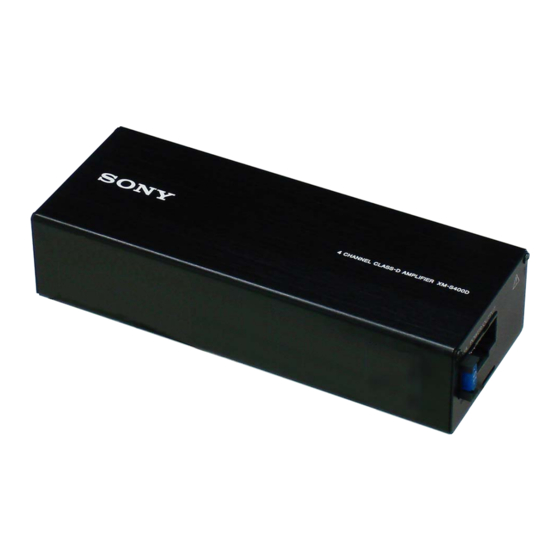
Sony XM-S400D Service Manual
4 channel class-d amplifier
Hide thumbs
Also See for XM-S400D:
- Operating instructions manual (16 pages) ,
- Operating instructions manual (160 pages) ,
- Operating instructions manual (15 pages)
Table of Contents
Advertisement
Quick Links
SERVICE MANUAL
Ver. 1.0 2015.10
FOR THE CUSTOMERS IN THE USA. NOT
APPLICABLE IN CANADA, INCLUDING IN THE
PROVINCE OF QUEBEC.
POUR LES CLIENTS AUX ÉTATS-UNIS. NON
AP PLICABLE AU CANADA, Y COMPRIS LA
PROVINCE DE QUÉBEC.
AUDIO POWER SPECIFICATIONS
CEA2006 Standard
Power Output: 45 Watts RMS × 4 at
4 Ohms < 1% THD+N
SN Ratio: 83 dBA
(reference: 1 Watt into 4 Ohms)
Circuit system
OTL (output transformerless) circuit,
Pulse power supply
Inputs
RCA pin jacks,
High level input connector
Input level
1 V (RCA pin jacks),
8 V (High level input)
9-896-237-01
Sony Video & Sound Products Inc.
2015J33-1
©
2015.10
Published by Sony Techno Create Corporation
SPECIFICATIONS
Outputs
Speaker terminals
Speaker impedance
4
– 8
Maximum output
4 Speakers: 100 W × 4 (at 4
)
Rated output
(supply voltage at 14.4 V, 1 kHz, 1% THD)
4 Speakers: 45 W × 4 (at 4
)
Frequency response
+0.5
20 Hz – 20 kHz (
dB)
−3.0
Harmonic distortion
0.08% or less (at 1 kHz, 4
)
Low-pass filter
120 Hz, 12 dB/oct
High-pass filter
120 Hz, 12 dB/oct
Power requirements
12 V DC car battery (negative ground (earth))
Power supply voltage
10.5 V – 16 V
Current drain
At rated output: 15 A (4
, 45 W × 4)
Remote input: 1 mA
NOTES ON CHIP COMPONENT REPLACEMENT
•
Never reuse a disconnected chip component.
•
Notice that the minus side of a tantalum capacitor may be dam-
aged by heat.
4 CHANNEL CLASS-D AMPLIFIER
XM-S400D
Canadian Model
Australian Model
Dimensions
Approx. 162.8 mm × 37.3 mm × 62.6 mm
1
1
(6
/
in × 1
/
in × 2
2
2
projecting parts and controls
37.3 mm (1
1
/
in)
2
62 .6 mm (2
1
/
in)
2
31.3 m m (1
1
/
in)
4
1
162.8 mm (6
/
in)
2
176.8 mm (7 in)
Mass
Approx. 0.46 kg (1
1
/
64
Package contents:
Main unit (1)
Parts for installation and connections (1 set)
Design and specifications are subject to change
without notice.
US Model
AEP Model
UK Model
E Model
1
/
in) (w/h/d) not incl.
2
lb) not incl. accessories
Advertisement
Table of Contents

Related Manuals for Sony XM-S400D


Summary of Contents for Sony XM-S400D
- Page 1 Never reuse a disconnected chip component. • Notice that the minus side of a tantalum capacitor may be dam- aged by heat. 4 CHANNEL CLASS-D AMPLIFIER 9-896-237-01 Sony Video & Sound Products Inc. 2015J33-1 © 2015.10 Published by Sony Techno Create Corporation...
-
Page 2: Section 1 Servicing Notes
XM-S400D SECTION 1 SERVICING NOTES The SERVICING NOTES contains important information for servicing. Be sure to read this section before repairing the unit. UNLEADED SOLDER DESTINATION ABBREVIATIONS Boards requiring use of unleaded solder are printed with the lead- The following abbreviations for model destinations are used in this free mark (LF) indicating the solder contains no lead. -
Page 3: Section 2 General
XM-S400D SECTION 2 This section is extracted GENERAL from instruction manual. Input Connections Power Connections Installation Set the INPUT SELECT switch to “2CH” or “4CH” Connect the +12 V power supply wire only after all Mount the unit on a flat surface. - Page 4 XM-S400D 2-way system High level input connection Speaker Connections Set with the input connection (page 7) or or D. Set the INPUT SELECT switch to “2CH” with the Set the REAR LPF switch and FRONT HPF switch to (page 8).
-
Page 5: Section 3 Disassembly
XM-S400D SECTION 3 DISASSEMBLY • This set can be disassembled in the order shown below. 3-1. DISASSEMBLY FLOW 3-2. CHASSIS BOTTOM BLOCK 3-3. HEAT TRANSFER SHEET (CHIP), MAIN BOARD (Page 5) (Page 6) Note: Follow the disassembly procedure in the numerical order given. - Page 6 XM-S400D 3-3. HEAT TRANSFER SHEET (CHIP), MAIN BOARD Note 1: When the complete MAIN board is replaced, be sure to apply the grease (OIL COMPOUND (KS609)) so as to cover the IC301 on the MAIN board. 1 two screws o itio o...
- Page 7 XM-S400D SECTION 4 DIAGRAMS 4-1. BLOCK DIAGRAM CN101 S103-1 SIGNAL FRONT INPUT POWER AMP DIFFERENTIAL HIGH-PASS IC301 CN501 BUFFER FILTER IC104 (1/2) IC101 (1/2) IC107 (1/2) FL– OUT2_P 15 IN2_P OUT2_M FL– R-CH FR– R-CH LOW-PASS FR– FILTER IC107 (2/2)
- Page 8 XM-S400D THIS NOTE IS COMMON FOR PRINTED WIRING BOARDS AND SCHEMATIC DIAGRAMS. • IC Block Diagrams (In addition to this, the necessary note is printed in each block.) – MAIN Board – For Printed Wiring Boards. For Schematic Diagrams. IC301 TAS5414CTPHDRQ1...
- Page 9 XM-S400D 4-2. PRINTED WIRING BOARD - MAIN Board - • : Uses unleaded solder. MAIN BOARD (SIDE A) (CHASSIS) (CHASSIS) R572 R569 R519 LND501 R571 R599 LND101 C509 R527 R575 R582 IC508 R526 R521 IC503 C528 C108 D101 C525 (CHASSIS)
- Page 10 XM-S400D 4-3. SCHEMATIC DIAGRAM - MAIN Board (1/3) - MAIN BOARD (1/3) C159 R145 R147 R152 C156 8.2k R134 C135 C138 R135 8.2k C133 2.7k 220p C145 R158 C154 8.2k R162 100V R126 R122 C151 100V C128 220p C127 220p...
-
Page 11: Main Board
XM-S400D 4-4. SCHEMATIC DIAGRAM - MAIN Board (2/3) - • See page 8 for IC Block Diagram. MAIN BOARD (2/3) C319 C321 C323 C325 C369 C368 0.01 R308 R314 C306 C311 R309 R315 C307 C312 RCH_GND C370 C352 R304 R307... - Page 12 XM-S400D 4-5. SCHEMATIC DIAGRAM - MAIN Board (3/3) - • See page 8 for Waveforms. • See page 8 for IC Block Diagrams. • See page 13 for IC Pin Function Description. MAIN BOARD (3/3) TP001 TP034 TP039 TP005 TH501...
- Page 13 XM-S400D • IC Pin Function Description MAIN BOARD IC508 R5F1037AANA (SYSTEM CONTROLLER) Pin No. Pin Name Description /RESET Reset signal input terminal “L”: reset Fixed at “H” in this unit BU_IN Battery voltage detection signal input terminal “L”: over voltage...
-
Page 14: Section 5 Exploded View
XM-S400D SECTION 5 EXPLODED VIEW Note: • -XX and -X mean standardized parts, so • The mechanical parts with no reference they may have some difference from the number in the exploded views are not sup- original one. plied. • Items marked “*” are not stocked since •... -
Page 15: Electrical Parts List
XM-S400D SECTION 6 MAIN ELECTRICAL PARTS LIST Note: • Due to standardization, replacements in • CAPACITORS When indicating parts by reference num- the parts list may be different from the uF: μF ber, please include the board name. parts specifi ed in the diagrams or the com- •... -
Page 16: Revision History
XM-S400D REVISION HISTORY Ver. Date Description of Revision 2015.10 How to search for a contact point of signal lines or the like in DIAGRAMS SECTION If a contact point of a BLOCK DIAGRAM, PRINTED WIRING BOARD or SCHEMATIC DIAGRAM is shown in a different page, use the PDF fi...
Need help?
Do you have a question about the XM-S400D and is the answer not in the manual?
Questions and answers