Sign In
Upload
Manuals
Brands
National Instruments Manuals
Computer Hardware
PXI-6508
National Instruments PXI-6508 Manuals
Manuals and User Guides for National Instruments PXI-6508. We have
1
National Instruments PXI-6508 manual available for free PDF download: User Manual
National Instruments PXI-6508 User Manual (88 pages)
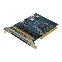
96-Bit and 24-Bit Parallel Digital I/O Interface for PCI, PXI, and CompactPCI
Brand:
National Instruments
| Category:
Computer Hardware
| Size: 1.86 MB
Table of Contents
Important Information
3
Table of Contents
4
About this Manual
8
Conventions
8
Related Documentation
9
Chapter 1 Introduction
10
About Your Board
10
Using PXI with Compactpci
11
What You Need to Get Started
11
Optional Equipment
12
Custom Cabling
12
Unpacking
13
Chapter 2 Installation and Configuration
14
Software Installation
14
Installing NI-DAQ
14
Installing Other Software
14
Hardware Installation
14
Installing the PCI-DIO-96 or PCI-6503
14
Installing the PXI-6508
15
Board Configuration
15
Chapter 3 Signal Connections
16
I/O Connector (PCI-DIO-96, PXI-6508)
16
I/O Connector Pin Assignments
16
Figure 3-1. PCI-DIO-96 and PXI-6508 Connector Pin Assignments
17
Cable Assembly Connectors
18
Figure 3-2. Cable-Assembly Connector Pinout for the R1005050
18
I/O Connector Signal Descriptions
19
Table 3-1. Signal Descriptions for PCI-DIO-96 and PXI-6508 I/O Connectors
19
I/O Connector (PCI-6503)
21
PCI-6503 I/O Connector Pin Descriptions
21
Figure 3-3. PCI-6503 I/O Connector Pin Assignments
21
Port C Pin Assignments
22
Table 3-2. PCI-6503 Signal Descriptions
22
Digital I/O Signal Connections
23
Table 3-3. Port C Signal Assignments
23
Figure 3-4. Digital I/O Connections Block Diagram
24
Power Connections
25
Digital I/O Power-Up State Selection
25
High DIO Power-Up State
25
Figure 3-5. DIO Channel Configured for High DIO Power-Up State with External Load
26
Low DIO Power-Up State (PXI-6508, PCI-6503 Only)
27
Figure 3-6. DIO Channel Configured for Low DIO Power-Up State with External Load
27
Chapter 4 Theory of Operation
29
Functional Overview
29
Figure 4-1. PCI-DIO-96/PXI-6508 Block Diagram
30
82C55A Programmable Peripheral Interface
31
PCI Interface Circuitry
31
Table 4-1. the 82C55A Chips Used in the PCI-DIO-96, PXI-6508
31
Timing Specifications
32
Table 4-2. Signal Names Used in Timing Diagrams
32
Figure 4-2. Timing Specifications for Mode 1 Input Transfer
33
Mode 1 Input Timing
33
Figure 4-3. Timing Specifications for Mode 1 Output Transfer
34
Mode 1 Output Timing
34
Figure 4-4. Timing Specifications for Mode 2 Bidirectional Transfer
35
Mode 2 Bidirectional Timing
35
Input Signals
36
Appendix A Specifications
37
Output Signals
37
Bus Interface
38
Shock and Vibration
40
Electromagnetic Compatibility
40
Appendix B Register-Level Programming
42
82C53 Programmable Interval Timer (PCI-DIO-96, PXI-6508 Only
43
Interrupt Control Circuitry
43
Figure B-1. Interrupt Control Circuitry Block Diagram
44
Register Map and Description
45
Introduction
45
Register Map
46
Table B-1. Register Address Map
46
Register Descriptions
47
Register Description for the 82C55A
47
Register Description Format
47
Figure B-2. Control Word Formats for the 82C55A
48
Table B-2. Port C Set/Reset Control Words
49
Register Description for the 82C53 (PCI-DIO-96, PXI-6508 Only
50
Figure B-3. Control Word Format for the 82C53
50
Register Description for the Interrupt Control Registers
51
Interrupt Control Register 1
51
Interrupt Control Register 2
53
Interrupt Clear Register (PCI-DIO-96, PXI-6508 Only
54
Programming
55
Pcl Local Bus
55
Programming Examples
55
PCI Initialization
56
Table B-3. Common Programming Example Terms
56
Programming Considerations for the 82C55A
58
Modes of Operation
58
Mode 0-Basic I/O
59
Table B-4. Mode 0 I/O Configurations
59
Mode 1-Strobed Input
60
Figure B-4. Control Word to Configure Port a for Mode 1 Input
60
Figure B-5. Control Word to Configure Port B for Mode 1 Input
61
Port C Status-Word Bit Definitions for Input (Ports a and B
62
Figure B-6. Port C Pin Assignments on I/O Connector When Port C Configured for Mode 1 Input
63
Mode 1-Strobed Output
64
Figure B-7. Control Word to Configure Port a for Mode 1 Output
64
Figure B-8. Control Word to Configure Port B for Mode 1 Output
64
Port C Status-Word Bit Definitions for Output (Ports a and B
65
Figure B-9. Port C Pin Assignments on I/O Connector When Port C Configured for Mode 1 Output
66
Mode 2-Bidirectional Bus
67
Port C Status-Word Bit Definitions for Bidirectional Data Path (Port a Only
68
Configured for Mode 2
69
Figure B-11. Port C Pin Assignments on I/O Connector When Port C Is Configured for Mode 2
69
Interrupt Handling
70
Interrupt Programming Examples for the 82C55A
70
General Information
71
Programming Considerations for the 82C53
71
Interrupt Programming Example
72
Appendix C Technical Support and Professional Services
73
Advertisement
Advertisement
Related Products
National Instruments PXI-6521
National Instruments PXI-6528
National Instruments PXI-6031E
National Instruments PXI-6602
National Instruments PXI-8423
National Instruments CAN PXI-8460
National Instruments NI Multifunction RIO PXI-7853R 8 AI
National Instruments NI PXI-8221
National Instruments DAQ X NI PXIe-6376
National Instruments DAQ X NI PXIe-6375
National Instruments Categories
Control Unit
I/O Systems
Controller
Computer Hardware
Measuring Instruments
More National Instruments Manuals
Login
Sign In
OR
Sign in with Facebook
Sign in with Google
Upload manual
Upload from disk
Upload from URL