
Related Manuals for National Instruments PCI-1200


Summary of Contents for National Instruments PCI-1200
- Page 1 NI PCI-1200 User Manual Multifunctional I/O Device for PCI Bus Computers NI PCI-1200 User Manual June 2002 Edition Part Number 320942D-01...
- Page 2 Sweden 08 587 895 00, Switzerland 056 200 51 51, Taiwan 02 2528 7227, United Kingdom 01635 523545 For further support information, see the Technical Support and Professional Services appendix. To comment on the documentation, send email to techpubs@ni.com. © 1996–2002 National Instruments Corporation. All rights reserved.
- Page 3 Warranty The NI PCI-1200 is warranted against defects in materials and workmanship for a period of one year from the date of shipment, as evidenced by receipts or other documentation. National Instruments will, at its option, repair or replace equipment that proves to be defective during the warranty period.
-
Page 4: Table Of Contents
National Instruments ADE Software...............1-3 Optional Equipment .......................1-3 Custom Cabling ......................1-4 Unpacking ........................1-4 Safety Information ......................1-5 Chapter 2 Installing and Configuring the NI PCI-1200 Installing the Software ....................2-1 Installing the Hardware....................2-1 Configuring the Device....................2-2 Analog I/O Configuration................2-2 Analog Output Polarity ..............2-3 Analog Input Polarity................2-3... - Page 5 Theory of Operation Functional Overview ..................... 4-1 PCI Interface Circuitry ....................4-2 Timing ........................... 4-3 Analog Input........................4-5 Analog Input Circuitry ..................4-6 DAQ Operations ..................... 4-7 Controlled Acquisition Mode ............4-8 Freerun Acquisition Mode..............4-8 NI PCI-1200 User Manual ni.com...
- Page 6 DAC Timing....................4-12 Digital I/O ........................4-12 Chapter 5 Calibration Calibration at Higher Gains ...................5-2 Calibration Equipment Requirements................5-2 Using the Calibration Function..................5-3 Appendix A Specifications Appendix B Technical Support and Professional Services Glossary Index © National Instruments Corporation NI PCI-1200 User Manual...
-
Page 7: About This Manual
The NI PCI-1200 is a low-cost multifunction analog, digital, and timing device. The NI PCI-1200 is a member of the National Instruments PCI Series of expansion devices for PCI bus computers. These devices are... -
Page 8: National Instruments Documentation
National Instruments plug-in DAQ devices. National Instruments Documentation The PCI-1200 User Manual is one piece of the documentation set for your DAQ system. You could have any of several types of manuals, depending on the hardware and software in your system. Use the manuals you have as follows: •... -
Page 9: Related Documentation
NI Developer Zone tutorial, Field Wiring and Noise Considerations for Analog Signals, located at ni.com/zone • PCI Local Bus Specification, Revision 2.2, available at pcisig.com • The technical reference manual for the computer © National Instruments Corporation NI PCI-1200 User Manual... -
Page 10: Introduction
Introduction This chapter describes the NI PCI-1200, lists what you need to get started, software programming choices, and optional equipment, and explains how to build custom cables and unpack the NI PCI-1200. About the NI PCI-1200 Thank you for purchasing the NI PCI-1200, a low-cost, high-performance multifunction analog, digital, and timing device for PCI bus computers. -
Page 11: Software Programming Choices
NI application development environment (ADE) or other ADEs. In either case, you use NI-DAQ. NI-DAQ NI-DAQ, which ships with the NI PCI-1200, has an extensive library of functions that you can call from the ADE. These functions allow you to use all the features of the NI PCI-1200. -
Page 12: National Instruments Ade Software
Using LabVIEW or Measurement Studio greatly reduces the development time for your data acquisition and control application. Optional Equipment NI offers a variety of products to use with the NI PCI-1200 device, including cables, connector blocks, and other accessories, as follows: •... -
Page 13: Custom Cabling
NI PCI-1200. Unpacking The NI PCI-1200 is shipped in an antistatic package to prevent electrostatic damage to the device. Electrostatic discharge (ESD) can damage several components on the device. To avoid such damage in handling the device,... -
Page 14: Safety Information
Notify NI if the device appears damaged in any way. Do not install a damaged device into your computer. Store the NI PCI-1200 in the antistatic envelope when not in use. Safety Information The following section contains important safety information that you must follow during installation and use of the product. - Page 15 MAINS is defined as the electricity supply system to which the equipment concerned is designed to be connected either for powering the equipment or for measurement purposes. NI PCI-1200 User Manual ni.com...
- Page 16 Chapter 1 Introduction Below is a diagram of a sample installation. © National Instruments Corporation NI PCI-1200 User Manual...
-
Page 17: Installing And Configuring The Ni Pci-1200
Install NI-DAQ according to the instructions on the CD and the DAQ Quick Start Guide included with the NI PCI-1200. It is important to install NI-DAQ before installing the NI PCI-1200 to ensure that Note the NI PCI-1200 is properly detected. -
Page 18: Configuring The Device
Chapter 2 Installing and Configuring the NI PCI-1200 Insert the NI PCI-1200 in an unused PCI system slot. The fit may be tight, but do not force the device into place. Screw the NI PCI-1200 mounting bracket to the back panel rail of the computer or use the slot side tabs, if available, to secure the NI PCI-1200 in place. -
Page 19: Analog Output Polarity
(4,095 decimal). Analog Input Polarity You can select the analog input on the NI PCI-1200 for either a unipolar range (0 to 10 V) or a bipolar range (–5 to +5 V). In addition, you can select the coding scheme for analog input as either two’s complement or straight binary. -
Page 20: Analog Input Mode
RSE Input Mode (Eight Channels, Reset Condition) RSE input means that all input signals are referenced to a common ground point that is also tied to the NI PCI-1200 AI ground. The differential amplifier negative input is tied to analog ground. RSE mode is useful for measuring floating signal sources. -
Page 21: Nrse Input Mode (Eight Channels)
NRSE Input Mode (Eight Channels) NRSE input means that all input signals are referenced to the same common-mode voltage, which floats with respect to the NI PCI-1200 analog ground. This common-mode voltage is subsequently subtracted by the input instrumentation amplifier. NRSE mode is useful for measuring ground-referenced signal sources. -
Page 22: Signal Connections
This chapter describes how to make input and output signal connections to the NI PCI-1200 through the device I/O connector and details the I/O timing specifications. The I/O connector for the NI PCI-1200 has 50 pins that you can connect to 50-pin accessories. I/O Connector Figure 3-1 shows the pin assignments for the NI PCI-1200 I/O connector. -
Page 23: Signal Connection Descriptions
DGND Figure 3-1. NI PCI-1200 I/O Connector Pin Assignments Signal Connection Descriptions The following table describes the connector pins on the NI PCI-1200 I/O connector by pin number and gives the signal name and description of each signal connector pin. - Page 24 Chapter 3 Signal Connections Table 3-1. Signal Descriptions for NI PCI-1200 I/O Connector Pins (Continued) Signal Name Direction Reference Description DAC0OUT AGND Digital-to-Analog Converter 0 Output—Voltage output signal for AO channel 0. AGND Analog Ground—AO ground reference for AO voltages. Bias current return point for differential measurements.
-
Page 25: Analog Input Signal Connections
AISENSE/AIGND, is an analog common signal. You can use this pin for a general analog power ground tie to the NI PCI-1200 in RSE mode or as a return path in NRSE mode. Pin 11, AGND, is the bias current return point for differential measurements. - Page 26 Caution Exceeding the input signal range distorts input signals. Exceeding the maximum input voltage rating may damage the NI PCI-1200 device and the computer. NI is not liable for any damage resulting from such signal connections. Table 3-2. Bipolar Analog Input Signal Range Versus Gain...
-
Page 27: Types Of Signal Sources
A/D conversions. All signals must be referenced to ground, either at the source device or at the NI PCI-1200. If you have a floating source, you must use a ground-referenced input connection at the NI PCI-1200. If you have a grounded source, use a nonreferenced input connection at the NI PCI-1200. -
Page 28: Ground-Referenced Signal Sources
The connection instructions that follow for grounded signal sources eliminate this ground potential difference from the measured signal. If you power both the NI PCI-1200 and the computer with a floating power source Note (such as a battery), the system may float with respect to earth ground. In this case, treat all of the signal sources as floating sources. - Page 29 Single-Ended — – Ground Referenced (RSE) AIGND Ground-loop losses, V , are added to measured signal. – AISENSE – AISENSE – – Single-Ended — Nonreferenced (NRSE) AIGND AIGND See text for information on bias resistors. NI PCI-1200 User Manual ni.com...
-
Page 30: Differential Connection Considerations (Diff Configuration)
When configuring the NI PCI-1200 for DIFF input, each signal uses two of the multiplexer inputs—one for the signal and one for its reference signal. -
Page 31: Differential Connections For Grounded Signal Sources
Figure 3-3. Differential Input Connections for Grounded Signal Sources With this connection type, the instrumentation amplifier rejects both the common-mode noise in the signal and the ground-potential difference between the signal source and the NI PCI-1200 ground (shown as V Figure 3-3). NI PCI-1200 User Manual 3-10 ni.com... -
Page 32: Differential Connections For Floating Signal Sources
Chapter 3 Signal Connections Differential Connections for Floating Signal Sources Figure 3-4 shows how to connect a floating signal source to a NI PCI-1200 configured for DIFF input mode. Configuration instructions are in the Analog I/O Configuration section of Chapter 2,... -
Page 33: Single-Ended Connection Considerations
• Input signals are high level (greater than 1 V). • Leads connecting the signals to the NI PCI-1200 are less than 10 ft. • All input signals share a common reference signal (at the source). If any of the preceding criteria is not met, use the DIFF input configuration. -
Page 34: Single-Ended Connections For Floating Signal Sources (Rse Configuration)
On the other hand, if the input circuitry of the NI PCI-1200 is referenced to ground, © National Instruments Corporation... -
Page 35: Common-Mode Signal Rejection Considerations
Common-Mode Signal Rejection Considerations Figures 3-4 and 3-6 show connections for signal sources that are already referenced to some ground point with respect to the NI PCI-1200. In these cases, the instrumentation amplifier can reject any voltage caused by ground-potential differences between the signal source and the NI PCI-1200. -
Page 36: Analog Output Signal Connections
Chapter 3 Signal Connections The common-mode input range for the NI PCI-1200 depends on the size of the differential input signal, V = (V +) – (V –), and the gain setting of diff the instrumentation amplifier. In unipolar mode, the differential input range is 0 to 10 V. -
Page 37: Digital I/O Signal Connections
Digital I/O Signal Connections Pins 13 through 37 of the I/O connector are DIO signal pins. DIO on the NI PCI-1200 uses the 82C55A integrated circuit. The 82C55A is a general-purpose peripheral interface containing 24 programmable I/O pins. These pins represent the three 8-bit ports (PA, PB, and PC) of the 82C55A. -
Page 38: Logical Inputs And Outputs
NI PCI-1200 Figure 3-8. Digital I/O Connections In Figure 3-8, port A is configured for digital output, and ports B and C are configured for digital input. Digital input applications include receiving © National Instruments Corporation 3-17 NI PCI-1200 User Manual... -
Page 39: Port C Pin Connections
Do not directly connect this +5 V power pin to analog or digital ground or to any other voltage source on the NI PCI-1200 or any other device. Doing so can damage the NI PCI-1200 or the computer. NI is not liable for any damage due to incorrect power connections. -
Page 40: Daq Timing Connections
EXTTRIG followed by a rising edge on EXTCONV*. The first conversion occurs on the next falling edge of EXTCONV*. Further transitions on the EXTTRIG line have no effect until a new DAQ sequence is established. © National Instruments Corporation 3-19 NI PCI-1200 User Manual... - Page 41 The sample counter has been programmed to allow five conversions after the rising edge on the EXTTRIG signal. Additional transitions on the EXTTRIG line have no effect until you initiate a new DAQ sequence. NI PCI-1200 User Manual 3-20 ni.com...
- Page 42 EXTCONV*. The GATE signal disables conversions for the rest of the scan interval after the desired channels have been scanned. Refer to the Interval Scanning Acquisition Mode section of Chapter 4, Theory of Operation, for more information on interval scanning. © National Instruments Corporation 3-21 NI PCI-1200 User Manual...
- Page 43 EXTUPDATE* bit. Therefore, you can perform externally timed, interrupt-driven waveform generation on the NI PCI-1200. The EXTUPDATE* line is susceptible to noise caused by switching lines and could generate false interrupts. You should make the width of the EXTUPDATE* pulse as short as possible, but greater than 50 ns.
-
Page 44: General Purpose Timing Signal Connections
You can enable or disable the counting operation by controlling the gate input. Figure 3-14 shows connections for a typical event-counting operation in which a switch is used to gate the counter on and off. © National Instruments Corporation 3-23 NI PCI-1200 User Manual... - Page 45 CLK input while the gate is applied. The frequency of the input signal then equals the count value divided by the gate period. Figure 3-15 shows the connections for a NI PCI-1200 User Manual 3-24 ni.com...
- Page 46 2.2 V min 5.3 V max – input logic low voltage –0.3 V min 0.8 V max –10 µA min +10 µA max – Input load current © National Instruments Corporation 3-25 NI PCI-1200 User Manual...
- Page 47 300 ns maximum outc output delay from gate 400 ns maximum outg Figure 3-16. General Purpose Timing Signals The GATE and OUT signals in Figure 3-16 are referenced to the rising edge of the CLK signal. NI PCI-1200 User Manual 3-26 ni.com...
-
Page 48: Timing Specifications
Acknowledge Input—A low signal on this handshaking line indicates that the data written from the specified port has been accepted. ACK* is primarily a response from the external device that it has received the data from the NI PCI-1200. OBF* Output Output Buffer Full—A low signal on this handshaking line indicates... -
Page 49: Mode 1 Input Timing
Data after STB* = 1 — RD* = 0 to INTR = 0 — RD* = 1 to IBF = 0 — All timing values are in nanoseconds. Figure 3-17. Mode 1 Timing Specifications for Input Transfers NI PCI-1200 User Manual 3-28 ni.com... -
Page 50: Mode 1 Output Timing
ACK* = 0 to OBF* = 1 — ACK* pulse width — ACK* = 1 to INTR = 1 — All timing values are in nanoseconds. Figure 3-18. Mode 1 Timing Specifications for Output Transfers © National Instruments Corporation 3-29 NI PCI-1200 User Manual... -
Page 51: Mode 2 Bidirectional Timing
ACK* = 0 to output — ACK* = 1 to output float RD* = 1 to IBF = 0 — All timing values are in nanoseconds. Figure 3-19. Mode 2 Timing Specifications for Bidirectional Transfers NI PCI-1200 User Manual 3-30 ni.com... -
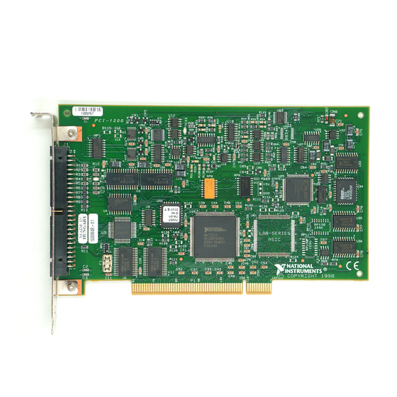
Page 52: Theory Of Operation
Group B 2 MHz Time 10 MHz Timebase Divider Oscillator Figure 4-1. NI PCI-1200 Block Diagram The major components of the NI PCI-1200 are as follows: • MITE PCI interface circuitry • TIO circuitry • AI circuitry • AO circuitry ©... -
Page 53: Pci Interface Circuitry
The NI PCI-1200 interface circuitry consists of the MITE PCI interface chip and a digital control logic chip. The MITE PCI interface chip provides a mechanism for the NI PCI-1200 to communicate with the PCI bus. It is an Application Specific Integrated Circuit (ASIC) designed by NI specifically for data acquisition. -
Page 54: Timing
Chapter 4 Theory of Operation The NI PCI-1200 generates an interrupt in the following five cases (each of these interrupts is individually enabled and cleared): • When a single A/D conversion can be read from the A/D FIFO memory •... - Page 55 Each 82C53 contains three independent 16-bit counter/timers and one 8-bit mode register. Each counter has a CLK input pin, a GATE input pin, and an OUT output pin. You can program all six counter/timers to operate in several timing modes. NI PCI-1200 User Manual ni.com...
-
Page 56: Analog Input
Analog Output sections. Analog Input The NI PCI-1200 has eight channels of analog input with software-programmable gain and 12-bit A/D conversion. The NI PCI-1200 also contains DAQ timing circuitry for automatic timing of multiple A/D conversions and includes advanced options such as external triggering, gating, and clocking. -
Page 57: Analog Input Circuitry
Gaussian noise to the signal to be converted to the ADC. This addition is useful for applications involving averaging, to increase the resolution of the NI PCI-1200 to more than 12 bits, as in calibration. In such applications, which are often lower frequency in nature, noise modulation is decreased and differential linearity is improved by the addition of the dither. -
Page 58: Daq Operations
This manual uses the phrase data acquisition operation (abbreviated as DAQ operation) to refer to a sequence of timed A/D conversions. The NI PCI-1200 performs DAQ operations in one of three modes: controlled acquisition mode, free-run acquisition mode, and interval scanning acquisition mode. -
Page 59: Controlled Acquisition Mode
Chapter 4 Theory of Operation Controlled Acquisition Mode The NI PCI-1200 uses two counters, counter A0 and counter A1, to execute DAQ operations in controlled acquisition mode. Counter A0 counts sample intervals, while counter A1 counts samples. In a controlled acquisition mode DAQ operation, the device performs a specified number of conversions, and then the hardware shuts off the conversions. -
Page 60: Single-Channel Data Acquisition
During each scan sequence, the NI PCI-1200 scans the start channel (the highest-numbered channel) first, then the next highest-numbered channel, and so on until it scans channel 0. The NI PCI-1200 repeats these scan sequences until the DAQ operation is terminated. - Page 61 2–10 13 µs typ, 16 µs max 15 µs typ, 19 µs max 27 µs typ, 34 µs max 60 µs typ, 80 µs max Table 4-2. NI PCI-1200 Maximum Recommended DAQ Rates Acquisition Mode Gain Rate Single-channel 1, 2, 5, 10, 20, 50, 100...
-
Page 62: Analog Output
Chapter 4 Theory of Operation Analog Output The NI PCI-1200 has two channels of 12-bit D/A output. Each AO channel can provide unipolar or bipolar output. The NI PCI-1200 also contains timing circuitry for waveform generation timed either externally or internally. -
Page 63: Dac Timing
24 programmable I/O pins. These pins represent the three 8-bit I/O ports (A, B, and C) of the 82C55A, as well as PA<0..7>, PB<0..7>, and PC<0..7> on the NI PCI-1200 I/O connector. Figure 4-6 shows the DIO circuitry. Data/Address Address PA<0..7>... -
Page 64: Calibration
The lower half of the EEPROM contains four user areas for calibration data. When the NI PCI-1200 is powered on, or the conditions under which it is operating change, you must load the calibration DACs with the appropriate calibration constants. -
Page 65: Calibration At Higher Gains
NI PCI-1200 as part of the NI-DAQ software. Calibration at Higher Gains The NI PCI-1200 has a maximum gain error of 0.8%. This means that if the device is calibrated at a gain of 1 and if the gain is switched to 100, a maximum error of 32 LSB may result in the reading. -
Page 66: Using The Calibration Function
RSE and for bipolar polarity, then configure the AO circuitry for the polarity at which you want to perform output waveform generation. Refer to your software documentation for more details on the function and the 1200 Calibrate VI. Calibrate_1200 © National Instruments Corporation NI PCI-1200 User Manual... -
Page 67: Appendix A Specifications
Specifications This appendix lists the NI PCI-1200 specifications. These specifications are typical at 25 °C unless otherwise stated. Analog Input Input Characteristics Number of channels ....... 8 single-ended, 8 pseudodifferential, or 4 differential, software-selectable Type of ADC.......... Successive-approximation Resolution ..........12 bits, 1 in 4,096 Max sampling rate........ - Page 68 DNL ............±1 LSB max No missing codes........12 bits, guaranteed Offset error Pregain error after calibration..10 µV max Pregain error before calibration..±20 mV max Postgain error after calibration ..1 mV max Postgain error before calibration ..±200 mV max NI PCI-1200 User Manual ni.com...
- Page 69 (Accuracy ±0.024% (±1 LSB)) 10 µs typ, 14 µs max 2–10 13 µs typ, 16 µs max 15 µs typ, 19 µs max 27 µs typ, 34 µs max 60 µs typ, 80 µs max © National Instruments Corporation NI PCI-1200 User Manual...
- Page 70 Integral nonlinearity (INL) in an ADC is an often ill-defined specification that should indicate the overall A/D transfer linearity of a converter. The manufacturer of the ADC chip NI uses on the NI PCI-1200 specifies its integral nonlinearity by stating that the analog center of any code does not deviate from a straight line by more than ±1 LSB.
- Page 71 NI has determined that the character of the noise in the NI PCI-1200 is fairly Gaussian, so the noise specifications given are the amounts of pure Gaussian noise required to produce our readings.
- Page 72 Before calibration ......±50 mV max Gain error (relative to internal reference) After calibration.......±0.01% of reading max Before calibration ......±1% of reading max Voltage Output Ranges ............0 to 10 V, ±5 V, software selectable Output coupling ........DC NI PCI-1200 User Manual ni.com...
- Page 73 0 LSBs (guaranteeing monotonicity) and is always less than 2 LSBs. Digital I/O Number of channels ....... 24 I/O (three 8-bit ports; uses 82C55A PPI) Compatibility ......... TTL © National Instruments Corporation NI PCI-1200 User Manual...
- Page 74 ±0.5 V powered off Resolution Counter/timers .........16 bits Compatibility ..........TTL Base clock available .......2 MHz Base clock accuracy........±50 ppm max Max source frequency......8 MHz Min source pulse duration ......125 ns Min gate pulse duration ......50 ns NI PCI-1200 User Manual ni.com...
- Page 75 Power available at I/O connector ... +4.65 to +5.25 V fused at 1 A Physical Dimensions..........17.45 by 10.56 cm (6.87 by 4.16 in.) I/O connector.......... 50-pin male Maximum Working Voltage Maximum working voltage refers to the signal voltage plus the common-mode voltage. © National Instruments Corporation NI PCI-1200 User Manual...
- Page 76 Humidity ..........5 to 90% RH, noncondensing Maximum altitude........2,000 meters Pollution degree (indoor use only) ..2 Safety The NI PCI-1200 meets the requirements of the following standards for safety and electrical equipment for measurement, control, and laboratory use: • EN 61010-1:1993/A2:1995, IEC 61010-1:1990/A2:1995 •...
- Page 77 Technical Support and Professional Services Visit the following sections of the National Instruments Web site at for technical support and professional services: ni.com • Support—Online technical support resources include the following: – Self-Help Resources—For immediate answers and solutions, visit our extensive library of technical support resources available in English, Japanese, and Spanish at .
- Page 78 ≥ greater than or equal to < less than – negative of, or minus ≠ not equal to Ω ohms percent ± plus or minus positive of, or plus +5 volts signal © National Instruments Corporation NI PCI-1200 User Manual...
- Page 79 CLKB1, CLKB2 counter B1, B2 clock signals centimeters CMRR common-mode rejection ratio—a measure of an instrument’s ability to reject interference from a common-mode signal, usually expressed in decibels (dB) CNTINT counter interrupt signal NI PCI-1200 User Manual ni.com...
- Page 80 V1/V2, for signals in volts direct current DGND digital ground signal digital input DIFF differential digital input/output direct memory access differential nonlinearity digital output © National Instruments Corporation NI PCI-1200 User Manual...
- Page 81 EXTUPDATE* external update signal farad FIFO first in first out memory buffer full-scale range feet GATB <0..2> counter B0, B1, B2 gate signals GATE gate signal hexadecimal hertz input/output input buffer full signal inches NI PCI-1200 User Manual ni.com...
- Page 82 NRSE nonreferenced single-ended mode—all measurements are made with respect to a common (NRSE) measurement system reference, but the voltage at this reference can vary with respect to the measurement system ground © National Instruments Corporation NI PCI-1200 User Manual...
- Page 83 DAQ device to keep a continuous buffer filled with data, so that when the trigger conditions are met, the sample includes the data leading up to the trigger condition read signal external resistance root mean square NI PCI-1200 User Manual ni.com...
- Page 84 © National Instruments Corporation NI PCI-1200 User Manual...
- Page 85 (2) a LabVIEW software module (VI), which consists of a front panel user interface and a block diagram program. volts, input high volts, input low positive/negative input voltage measured voltage Vrms volts, root-mean-square signal source watts WRT* write signal NI PCI-1200 User Manual ni.com...
- Page 86 (table), 4-10 single-ended connections for input modes. See analog input modes ground-referenced signal polarity sources, 3-13 configuration, 2-3 settings (table), 2-2 definition (table), 2-4 purpose and use, 2-4 © National Instruments Corporation NI PCI-1200 User Manual...
- Page 87 A-1 CLKB1 signal (table), 3-4 stability, A-4 CLKB2 signal (table), 3-4 transfer characteristics, A-2 CNTINT signal, 3-22 analog output common mode signal rejection circuitry, 4-11 considerations, 3-14 DAC timing, 4-12 NI PCI-1200 User Manual © National Instruments Corporation...
- Page 88 I/O signal connections single-channel data acquisition, 4-9 figure, 3-17 DAQ rates, 4-9 logical inputs and outputs, 3-17 explanation, A-6 pins, 3-16 maximum recommended rates Port C pin connections, 3-18 (table), 4-10 © National Instruments Corporation NI PCI-1200 User Manual...
- Page 89 GATE, CLK, and OUT signals, 3-23 definition (table), 3-3 pins, 3-18 maximum voltage input rating, 3-23 pulse and square wave generation, 3-23 EXTUPDATE* signal pulse-width measurement, 3-24 DAQ timing, 3-22 specifications and ratings, 3-25 definition (table), 3-3 NI PCI-1200 User Manual © National Instruments Corporation...
- Page 90 4-6 configuration mux counters, 4-6 installation hardware installation, 2-1 software installation, 2-1 National Instruments unpacking the NI PCI-1200, 1-4 customer education, B-1 instrument drivers, B-1 professional services, B-1 instrumentation amplifier system integration services, B-1 figure, 3-6 technical support, B-1...
- Page 91 A-9 OBF* signal (table), 3-27 pin assignments for I/O connector (figure), 3-2 online technical support, B-1 polarity operation of PCI-1200. See theory of operation analog input, 2-3 OUT signals analog output, 2-3 general-purpose timing signal settings (table), 2-2...
- Page 92 4-11 power connections, 3-18 figure, 4-11 signal descriptions (table), 3-2 DAC timing, 4-12 single-channel data acquisition, 4-9 block diagram of NI PCI-1200, 4-1 single-ended connections digital I/O, 4-12 floating signal sources (RSE configuration), 3-13 circuitry (figure), 4-12 ground-referenced signal sources (NRSE...
- Page 93 B-1 interval scanning, 3-21 pins, 3-18 posttrigger and pretrigger unipolar signal range vs. gain (table), 3-5 modes, 3-19 unpacking the NI PCI-1200, 1-4 posttrigger timing (figure), 3-20 pretrigger timing (figure), 3-21 general-purpose timing signal connections waveform generation timing sequence, 3-22...