Sign In
Upload
Manuals
Brands
GOWIN Manuals
Receiver
GW2AR Series
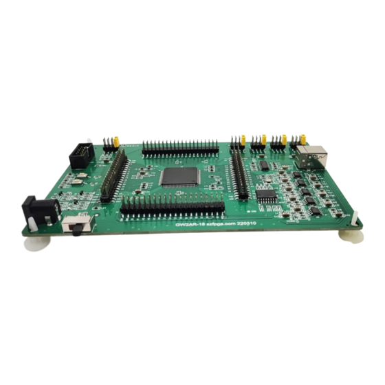
GOWIN GW2AR Series Manuals
Manuals and User Guides for GOWIN GW2AR Series. We have
7
GOWIN GW2AR Series manuals available for free PDF download: Programming And Configuration Manual, Programming And Configuraion Manual, User Manual, Manual, Schematic Manual
GOWIN GW2AR Series Programming And Configuration Manual (108 pages)
Brand:
GOWIN
| Category:
Semiconductors
| Size: 2 MB
Table of Contents
Table of Contents
4
List of Figures
6
About this Guide
10
Purpose
10
Related Documents
10
Terminology and Abbreviations
10
Table 1-1 Abbreviations and Terminology
10
Support and Feedback
11
Glossary
12
Table 2-1 Glossary
12
Configuration Modes
14
Littlebee ® Family of FPGA Products
14
Table 3-1 Configuration Modes
15
Table 3-2 Configuration Modes
15
Arora Family of FPGA Products
16
Configuration Process
17
Power-Up Sequence
19
Figure 4-1 por Power-Up Timing
19
Table 4-1 Power Rails Monitored by por Circuits of Different Devices
19
Initialization
20
Configuration
20
Wake-Up
20
User Mode
21
Configuration Pin
22
Configuration Pin List and Reuse Options
22
Configuration Pin List
22
Table 5-1 Configuration Pin List
22
Configuration Pin Reuse
23
Table 5-2 Pin Reuse Options
24
Configuration Pin Function and Application
25
Figure 5-1 Configuring Pin Reuse
25
Table 5-3 Pin Function
25
Figure 5-2 MCLK Frequency Setting
28
Configuration Mode Introduction
30
Configuration Notes
30
Figure 6-1 Recommended Pin Connection
32
Figure 6-2 Power Recycle Timing
33
Figure 6-3 Trigger Timing
33
Table 6-1 Timing Parameters for Cycling Power and RECONFIG_N Trigger
33
JTAG Configuration
34
JTAG Configuration Mode Pins
34
Table 6-2 Timing Parameters for Power-On Again and RECONFIG_N Triggering (Arora Family)
34
Table 6-3 Pin Description in JTAG Configuration Mode
34
Connection Diagram for the JTAG Configuration Mode
35
Figure 6-4 Connection Diagram for JTAG Configuration Mode
35
JTAG Configuration Timing
36
Figure 6-5 Connection Diagram of JTAG Daisy-Chain Configuration Mode
36
Figure 6-6 JTAG Configuration Timing
36
Table 6-4 JTAG Configuration Timing Parameters
36
JTAG Configuration Process
37
Figure 6-7 TAP State Machine
37
Figure 6-8 Instruction Register Access Timing
38
Figure 6-9 Data Register Access Timing
38
Table 6-5 Gowin FPGA IDCODE
38
Table 6-6 Change of TDI and TMS Value in the Process of Sending Instructions
39
Figure 6-10 Read Machine Flow Chart in ID Code State
40
Figure 6-11 the Access Timing of Read ID Code Instruction- 0X11
40
Figure 6-12 Read ID Code Data Register Access Timing
40
Figure 6-13 SRAM Configuration Flow
42
Table 6-7 Count of Address and Length of One Address
43
Figure 6-14 Process of Reading SRAM
44
Figure 6-15 Process of Normal Programming
46
Figure 6-16 Process of Background Programming
47
Table 6-8 TCK Frequency Requirements for JTAG
47
Figure 6-17 the Embedded Flash Erasing Process of T Technology
49
Figure 6-18 the Embedded Flash Erasing Process of H Technology
51
Table 6-9 Readback-Pattern / Autoboot-Pattern
52
Figure 6-19 Process of Programming Internal Flash View
53
Figure 6-20 X-Page Programming
54
Figure 6-21 Y-Page Programming
55
Figure 6-22 Process of Reading Internal Flash
56
Figure 6-23 Process of Reading a Y-Page
57
Figure 6-24 GW1N-4 Background Programming Flow
58
Figure 6-25 Transfer JTAG Instruction Sample & Extest Flow Chart
59
Figure 6-26 Connection Diagram of JTAG Programming External Flash
60
Figure 6-27 Process View of Programming SPI Flash SPI
60
Figure 6-28 Timing Diagram of Sending 0X06 Via GW2A Series JTAG Simulating SPI
61
Figure 6-29 Timing Diagram of Sending 0X06 Via GW1N Series JTAG Simulating SPI
61
Table 6-10 Pin State
61
Figure 6-30 Process of Use Boundary Scan Mode to Program SPI Flash
62
Table 6-11 Status Register Definition
63
AUTO BOOT Configuration (Supported by Littlebee Family Only)
64
Figure 6-31 Connection Diagram of Daisy-Chain
64
Sspi
66
SSPI Mode Pins
66
Table 6-12 SSPI Mode Pins
66
SSPI Configuration Timing
67
Configuration Instruction
67
Figure 6-32 SSPI Configuration Timing
67
Table 6-13 SSPI Configuration Timing Parameters
67
Figure 6-33 Read ID Code Timing
68
Table 6-14 Configuration Instruction
68
Figure 6-34 Write Enable (0X15) Timing
69
Figure 6-35 Write Disable(0X3A00) Timing
69
Figure 6-36 Write Data (0X3B) Timing
70
Connection Diagram for SSPI Configuration Mode
71
Figure 6-37 SSPI Configuration Mode Connection Diagram
71
Figure 6-38 Connection Diagram of Programming External Flash Via SSPI
71
Multiple FPGA Connection View in SSPI Mode
72
Figure 6-39 the Flow of Programming External Flash Via SSPI
72
Figure 6-40 Multiple FPGA Connection Diagram 1
72
Figure 6-41 Multiple FPGA Connection Diagram 2
72
Mspi
73
MSPI Mode Pins
74
Table 6-15 Pin Description in MSPI Configuration Mode
74
Connection Diagram for MSPI Configuration Mode
75
Figure 6-42 Connection Diagram for MSPI Configuration Mode
75
Figure 6-43 Connection Diagram of JTAG Programming External Flash
75
MSPI Mode Configuration Attempts
76
Multi Boot
76
Figure 6-44 Example of Bitstream Image Distribution in Flash Memory
77
Figure 6-45 Input the Start Address for the Next Bitstream
78
Figure 6-46 Set the Programming Address for the External Flash
79
MSPI Configuration Timing
80
Figure 6-47 Connection Diagram for Configuring Multiple Fpgas Via Single Flash
80
Figure 6-48 MSPI Download Timing
80
DUAL BOOT Configuration (Supported by Littlebee Family Only)
81
Figure 6-49 Multiple FPGA Connection Diagram in MSPI Configuration Mode
81
Table 6-16 MSPI Configuration Timing Parameters
81
Figure 6-50 Dual Boot Flow Chart
82
CPU Mode
83
Table 6-17 CPU Mode Pins
83
Configuration Timing
84
SERIAL Mode
84
Figure 6-51 Connection Diagram for CPU Mode
84
Figure 6-52 CPU Mode Configuration Timing
84
Figure 6-53 Connection Diagram for SERIAL Mode
85
Figure 6-54 SERIAL Configuration Timing
85
Table 6-18 Pin Definition in SERIAL Configuration Mode
85
I 2 C Mode
86
Table 6-19 SERIAL Configuration Timing Parameters
86
Table 6-20 Pin Definition in SERIAL Configuration Mode
86
Figure 6-55 Connection Diagram for I 2 C Mode
87
Figure 6-56 I 2 C Mode Timing
87
Table 6-21 I 2 C Configuration Timing Parameters
87
Process of GW1N-2 Configuring or Programming Sram/Flash
89
Figure 6-57 Process of GW1N-2 Configuring or Programming Sram/Flash
89
Bitstream File Configuration
90
Configuration Options
90
Configuration Data Encryption (Supported by Arora Family Only)
91
Definition
91
Figure 7-1 Configuration Options
91
Enter Encryption KEY
92
Enter the Decrypt Key
92
Figure 7-2 Encryption Key Setting Method
92
Programming Operation
93
Figure 7-3 Setting the Decryption Key
93
Figure 7-4 AES Security Configure
94
Programming Flow
95
Figure 7-5 Prepare
95
Figure 7-6 Read AES Key Flow
96
Figure 7-7 Program AES Key Flow
97
Configuration File Size
98
Figure 7-8 Lock AES Key Flow
98
Figure 7-9 Bitstream Format Generation
99
Table 7-1 Gowin FPGA Products Configuration File Size (Max.)
99
Configuration File Loading Time
100
Table 7-2 Loading Frequency of Config File
101
Table 7-3 Loading Time in MSPI Mode
102
Safety Precautions
103
Boundary Scan
105
Figure 9-1 Boundary Scan Operation Schematic Diagram
106
SPI Flash Selection
107
Advertisement
GOWIN GW2AR Series Programming And Configuraion Manual (58 pages)
FPGA products
Brand:
GOWIN
| Category:
Semiconductors
| Size: 0 MB
Table of Contents
Table of Contents
4
List of Figures
6
About this Guide
8
Purpose
8
Supported Products
8
Related Documents
8
Abbreviations and Terminology
9
Support and Feedback
9
Table 1-1 Abbreviations and Terminology
9
Glossary
10
Table 2-1 Glossary
10
Configuration Mode and Power-On Requirements
12
GW1N(R/S) Series of FPGA Products
12
Configuration Modes
13
Power Supply Voltage
13
Table 3-1 Configuration Modes
13
GW2A(R) Series of FPGA Products
14
Configuration Modes
14
Table3-2 Recommended Power Supply Voltage
14
Table 3-3 Configuration Modes
14
Power Supply Voltage
15
Table3-4 Recommended Power Supply Voltage
15
Configuration Pin
16
Configuration Pin List and Reuse Options
16
Pin Multiplexing
17
Table 4-1 Configuration Pin List
17
Table 4-2 Pin Reuse Options
18
Pin Function and Application
19
Figure 4-1 Configuring Pin Reuse
19
Table 4-3 Pin Function
19
Figure 4-2 MCLK Frequency Setting
24
Configuration Mode
25
Configuration Notes
26
Figure 5-1 Recommended Pin Connection
27
Figure 5-2 Power Recycle Timing
28
Table 5-1Corresponding MODE Value
28
Figure 5-3 Trigger Timing
29
Table 5-2 Timing Parameters for Cycling Power and RECONFIG_N Trigger
29
Table 5-3 Timing Parameters for Cycling Power and RECONFIG_N Trigger
29
JTAG Configuration
30
Table 5-4 Pin Description in JTAG Configuration Mode
30
Figure 5-4 Connection Diagram for the JTAG Configuration Mode
31
Figure 5-5 Connection Diagram of JTAG Daisy-Chain Configuration Mode
32
Figure5-6 JTAG Configuration Timing
32
Table 5-5 JTAG Configuration Timing Parameters
32
AUTO BOOT Configuration (Supported by GW1N(R/S) Only)
33
Sspi
34
Figure 5-7 SSPI Configuration Mode Connection Diagram
34
Table 5-6 SSPI Mode Pins
34
Figure 5-8 SSPI Programming Via External Flash Connection Diagram
35
Figure 5-9 JTAG Configuration Timing
35
Mspi
36
Table 5-7 SSPI Configuration Timing Parameters
36
Table 5-8 Pin Description in JTAG Configuration Mode
37
Figure 5-10 MSPI Configuration Mode Connection Diagram
38
Figure 5-11 Connection Diagram of JTAG Programming External Flash
38
Figure 5-12 Input the Start Address for the Next Bitstream
40
Figure 5-13 Set the Programming Address for the External Flash
41
Figure 5-14 Connection Diagram for Configuring Multi-Chip FPGA Via Single Flash
42
Figure5-15 MSPI Download Timing
42
Table 5-9 MSPI Configuration Timing Parameters
42
AUTO BOOT Configuration (Supported by GW1N(R/S) Only)
43
Figure 5-16 Dual Boot Flow Chart
44
CPU Mode
45
Figure 5-17 Connection Diagram for the CPU Mode
45
Table 5-10 CPU Mode Pins
45
Serial
46
Figure 5-18 Connection Diagram for the SERIAL Mode
46
Table 5-11 Pin Definition in SERIAL Configuration Mode
46
Bitstream File Configuration
48
Configuration Options
49
Data Encryption (Supported by GW2A(R) Series Only)
49
Figure 6-1 Configuration Options
49
Figure 6-2 Encryption Key Setting Method
50
Figure 6-3 Setting the Decryption Key
51
Configuration File Size
52
Figure 6-4Bitstream Format Conversion Tool
52
Table 6-1 Gowin FPGA Products Configuration File Size
52
Safety Precautions
53
Boundary Scan
55
Figure 8-1 Boundary Scan Operation Schematic Diagram
56
SPI Flash Selection
57
Table 9-1 SPI Flash Operation Instruction
57
GOWIN GW2AR Series User Manual (33 pages)
Package & Pinout
Brand:
GOWIN
| Category:
I/O Systems
| Size: 1 MB
Table of Contents
Table of Contents
4
List of Figures
5
About this Guide
7
Purpose
7
Related Documents
7
Abbreviations and Terminology
7
Table 1-1 Abbreviations and Terminology
7
Support and Feedback
8
Overview
9
PB-Free Package
9
Max. I/O Information and LVDS Pair
10
Power Pin
10
Table 2-1 Max. I/O Information and LVDS Pair
10
Table 2-2 GW2AR Power Pin
10
Pin Quantity
11
Table 2-3 Quantity of GW2AR-18 Pins (Devices Embedded with SDRAM)
11
Table 2-4 Quantity of GW2AR-18 Pins (Devices Embedded with PSRAM)
12
Introduction to the I/O BANK
14
Figure 2-1 GW2AR I/O Bank Distribution
14
View of Pin Distribution
15
GW2AR-18 Pins Distribution View
15
View of QN88 Pins Distribution (Embedded with SDRAM)
16
Figure 3-1 View of GW2AR-18 QN88 Pins Distribution (Embedded with SDRAM)
16
Table 3-1 Other Pins in GW2AR-18 QN88 (Embedded with SDRAM)
16
View of QN88P Pins Distribution (Embedded with PSRAM)
17
Figure 3-2 View of GW2AR-18 QN88P Pins Distribution (Embedded with PSRAM)
17
Table 3-2 Other Pins in GW2AR-18 QN88P (Embedded with PSRAM)
17
View of QN88PF Pins Distribution (Embedded with PSRAM)
19
Figure 3-3 View of GW2AR-18 QN88PF Pins Distribution (Embedded with PSRAM)
19
Table 3-3 Other Pins in GW2AR-18 QN88PF (Embedded with PSRAM)
19
View of LQ144/EQ144 Pins Distribution (Embedded with SDRAM)
20
Figure 3-4 GW2AR-18 LQ144/EQ144 Pins Distribution View (Embedded with SDRAM)
20
Table 3-4 Other Pins in GW2AR-18 LQ144/EQ144 (Embedded with SDRAM)
20
View of EQ144P Pins Distribution (Embedded with PSRAM)
22
Figure 3-5 GW2AR-18 EQ144P Pins Distribution View (Embedded with PSRAM)
22
Table 3-5 Other Pins in GW2AR-18 EQ144P (Embedded with PSRAM)
22
View of EQ144PF Pins Distribution (Embedded with PSRAM)
23
Figure 3-6 GW2AR-18 EQ144PF Pins Distribution View (Embedded with PSRAM)
23
Table 3-6 Other Pins in GW2AR-18 EQ144PF (Embedded with PSRAM)
23
View of LQ176/EQ176 Pins Distribution (Embedded with SDRAM)
25
Figure 3-7 GW2AR-18 LQ176/EQ176 Pins Distribution View (Embedded with SDRAM)
25
Table 3-7 Other Pins in GW2AR-18 LQ176/EQ176 (Embedded with SDRAM)
25
Package Diagrams
27
QN88/QN88P/QN88PF Package Outline (10Mm X 10Mm)
28
Figure 4-1 Package Outline QN88/QN88P
28
LQ144 Package Outline (20Mm X 20Mm)
29
Figure 4-2 Package Outline LQ144
29
EQ144/ EQ144P/EQ144PF Package Outline (20Mm X 20Mm)
30
Figure 4-3 Package Outline EQ144
30
EQ176 Package Outline (20Mm X 20Mm)
31
Figure 4-4 Package Outline EQ176
31
LQ176 Package Outline (20Mm X 20Mm)
32
Figure 4-5 Package Outline LQ176
32
Advertisement
GOWIN GW2AR Series User Manual (23 pages)
Brand:
GOWIN
| Category:
Receiver
| Size: 0 MB
Table of Contents
User Guide
1
Table of Contents
4
Contents
5
List of Figures
6
1 About this Manual
8
Manual Content
8
Applicable Products
8
Related Documents
8
Terms and Abbreviations
8
Table 1-1 Terms and Abbreviations
8
Technical Support and Feedback
9
2 Function Introduction
10
Overview
10
Features
10
Gowin UART Master IP
10
Gowin UART Slave IP
10
3 Signal Definition
11
Gowin UART Master IP
11
SRAM Interface Signal
11
UART Side Signal
11
Table3-1 SRAM Interface Signal Definition
11
Table3-2 UART Side Signal Definition
11
Gowin UART Slave IP
12
Table3-3 UART Slave Signal Definition
12
4 Working Principle
13
System Diagram
13
Gowin UART Master IP Register
13
Figure 4-1 System Diagram
13
Receive Buffer Register (RBR)
14
Transmit Holding Register (THR)
14
Interrupt Enable Register (IER)
14
Figure4-2 Receive Buffer Register
14
Figure4-3 Transmit Holding Register
14
Table4-1 Gowin UART Master IP Register
14
Table4-2 Receive Buffer Register Bit Definition
14
Table4-3 Transmit Holding Register Bit Definitions
14
Interrupt Identification Register (IIR)
15
Figure 4-4 Interrupt Enable Register
15
Figure 4-5 Interrupt Identification Register
15
Table4-4 Interrupt Enable Register Bit Definition
15
Table4-5 Interrupt Identification Register Bit Definition
15
Line Control Register (LCR)
16
Modem Control Register (MCR)
16
Figure4-6 Line Control Register
16
Figure 4-7 Modem Control Register
16
Table4-6 Line Control Register
16
Table4-7 Modem Control Register
16
Line Status Register (LSR)
17
Figure4-8 Line Status Register
17
Table4-8 Line Status Register
17
Modem Status Register (MSR)
18
Figure4-9 Modem Status Register
18
Table4-9 Modem Status Register
18
Gowin UART Slave Implementation
19
Figure4-10 UART Slave Implementation Block Diagram
19
5 Interface Configuration
20
UART MASTER IP Core Interface
20
Figure5-1 UART MASTER Configuration Interface
20
UART SLAVE IP Core Interface
21
Figure 5-2 UART SLAVE Configuration Interface
21
GOWIN GW2AR Series User Manual (22 pages)
Brand:
GOWIN
| Category:
Motherboard
| Size: 0 MB
Table of Contents
Table of Contents
4
Contents
5
List of Figures
6
About this Guide
8
Purpose
8
Supported Products
8
Related Documents
8
Abbreviations and Terminology
9
Support and Feedback
9
Introduction
10
Device Table
10
Figure 2-1 Gowin Programmer
10
Output Panel
11
Table 2-1 Device Table
11
Programming Download
12
Download Cable Setting
12
Figure 3-1 Operation Process of Programming Download
12
Create New Project
13
Open Existing Project
13
Figure 3-2 Cable Setting
13
Table 3-1 Cable Setting Parameters
13
Scan Daisy Chain
14
Daisy Chain Configuration
14
Add Device
14
Figure 3-3 Device Table
14
Remove Device
16
Modify Device Position in Chain
16
Device Programming Configuration
16
Figure 3-4 Device Configuration
16
Table 3-2 Device Configuration Parameters
17
Table 3-3 Device Programming Configuration
17
SRAM Configuration
18
Embflash Configuration - GW1N (R) Series of FPGA Products
18
Exflash Configuration
18
Edit Pin State
19
Figure 3-5 I/O State Editor
19
Key Programming
20
Check the Current Configuration
20
Figure 3-6 Security Configuration
20
Table 3-4 Security Configuration Parameters
20
Save the Current Configuration to the Project File
21
Download Program
21
Figure 3-7 File Convertor
21
GOWIN GW2AR Series Manual (15 pages)
FPGA Products
Brand:
GOWIN
| Category:
Computer Hardware
| Size: 0 MB
GOWIN GW2AR Series Schematic Manual (15 pages)
Brand:
GOWIN
| Category:
Microcontrollers
| Size: 0 MB
Advertisement
Related Products
GOWIN GW2A Series
GOWIN GW2A-55
GOWIN GW2A-18
GOWIN GW2AR-18
GOWIN GW1N Series
GOWIN GW1NR Series
GOWIN GW1N-2
GOWIN GW1N-2B
GOWIN GW1N-4
GOWIN GW1N-6
GOWIN Categories
Motherboard
Semiconductors
Computer Hardware
Microcontrollers
Recording Equipment
More GOWIN Manuals
Login
Sign In
OR
Sign in with Facebook
Sign in with Google
Upload manual
Upload from disk
Upload from URL