Sign In
Upload
Manuals
Brands
Advantech Manuals
Computer Hardware
SOM-5992
Advantech SOM-5992 Manuals
Manuals and User Guides for Advantech SOM-5992. We have
2
Advantech SOM-5992 manuals available for free PDF download: Design Manual, User Manual
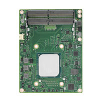
Advantech SOM-5992 Design Manual (129 pages)
COM Express, COMe TYPE7
Brand:
Advantech
| Category:
Single board computers
| Size: 4 MB
Table of Contents
Table of Contents
2
1 Introduction
9
About this Document
9
Acronyms / Definitions
9
Table 1: Acronyms / Definitions Signal Table Terminology Descriptions
9
Reference Documents
13
Revision History
13
SOM-5992 Block Diagram
14
Figure 1: SOM-5992 Block Diagram
14
Module Pin-Out Types 7 - Required and Optional Features
15
Table 2: Module Pin-Out - Required and Optional Features
15
2 COM Express Type 7 Interfaces
17
COM Express Type 7 Connector Layout
17
Figure 2: COM Express Type7 Connector Layout
17
COM Express Type 7 Connector Pin-Out
18
Table 3: COM Express Type 7 Pin-Out
18
General Purpose PCI Express Lanes
26
General Purpose Pcie Signal Definitions
26
Table 4: General Purpose PCI Express Signal Descriptions
26
PCI Express General Routing Guidelines
38
PCI Express Insertion Loss Budget with Slot Card
38
Figure 3: PCI Express Insertion Loss Budget with Slot Card
38
Table 6: PCI Express Insertion Loss Budget, 1.25 Ghz with Carrier Board Slot Card
39
PCI Express Insertion Loss Budget with Carrier Board PCIE Device
40
Table 7: PCI Express Insertion Loss Budget, 2.5 Ghz with Carrier Board Slot Card
40
Figure 4: PCI Express Insertion Loss Budget with Carrier Board Pcie Device
40
Table 8: PCI Express Insertion Loss Budget, 1.25 Ghz with Carrier Board Pcie Device
41
Table 9: PCI Express Insertion Loss Budget, 2.5 Ghz with Carrier Board Pcie Device
41
PCI Express Trace Length Guidelines
42
Figure 5: Topology for PCI Express Slot Card
42
Figure 6: Topology for PCI Express Device down
42
Table 10: PCI Express* Slot Card / Device down Trace Length Guidelines
43
Nc-Si
44
NC-SI Signal Definitions
44
Table 11: NC-SI Signal Description
44
NC-SI General Routing Guidelines
45
NC-SI Trace Length Guidelines
45
Table 12: NC-SI Trace Length Guidelines
45
Figure 7: Topology for NC-SI
45
10GB Ethernet
46
10GB LAN Signal Definitions
47
Table 13: 10GB LAN Signal Description
47
Table 14: I2C Data Mapping to Carrier Board Based PCA9539 I/O Expander
54
Example 10 GB Ethernet Designs
55
2016 Silicon 10Gbe Fiber Implementation
55
Figure 8: 10G Ethernet Design for Fiber PHY with Broadwell de
55
2016 Silicon 10Gbe Copper Implementation
56
Figure 9: 10G Ethernet Design for Copper PHY with Broadwell de
56
Future Silicon 10Gbe Fiber Implementation
57
Figure 10: 10G Ethernet Design for Fiber PHY with Future Soc
57
Future Silicon 10Gbe Copper Implementation
58
Figure 11: 10G Ethernet Design for Copper PHY with Future Soc
58
AC Coupling of 10G_KR_TX Signals
59
Figure 12: 10G Ethernet AC Coupling - Backplane System
59
Figure 13: 10G Ethernet AC Coupling - Direct Cable
59
Figure 14: 10G Ethernet AC Coupling - PHY on Carrier
59
10GB LAN Routing Guidelines
60
Figure 15: 10GBASE-KR Trace Length Budget
60
Table 15: 10/100/1000 Ethernet Insertion Loss Budget, 100 Mhz
60
10GB LAN KR Guidelines
61
Table 16: 10GB LAN KR Trace Length Guidelines
61
10GB LAN Sideban Guidelines
62
Table 17: 10GB LAN Sideban Trace Length Guidelines
62
Gb Ethernet
63
Gb Ethernet Signal Definitions
63
Table 18: Gb Ethernet Interface Signal Descriptions
63
SDP Pins
65
Gb Ethernet Routing Guidelines
66
Table 19: 10/100/1000 Ethernet Insertion Loss Budget, 100 Mhz
66
Figure 16: 10/100/1000 Ethernet Insertion Loss Budget
66
Gb Ethernet Trace Length Guidelines
67
Table 20: Ethernet Trace Length Guidelines
67
Figure 17: Topology for Ethernet Jack
67
Reference Ground Isolation and Coupling
68
USB2.0 Ports
69
USB2.0 Signal Definitions
69
Table 21: USB Signal Descriptions
69
Powering USB Devices During S5
71
USB Over-Current Protection (Usb_X_Y_Oc#)
71
USB2.0 Routing Guidelines
72
Figure 18: USB 2.0 Insertion Loss Budget
72
Table 22 :USB Insertion Loss Budget, 400 Mhz
72
USB 2.0 General Design Considerations and Optimization
73
USB 2.0 Port Power Delivery
73
Figure 19: USB 2.0 Good Downstream Power Connection
74
Figure 20: USB 2.0 a Common Mode Choke
74
USB 2.0 Common Mode Chokes
74
EMI / ESD Protection
75
USB2.0 Trace Length Guidelines
76
Table 23: USB2.0 Trace Length Guidelines
76
Figure 21: Topology for USB2.0
76
Usb3.0
77
USB3.0 Signal Definitions
77
Table 24: USB3.0 Signal Definitions
77
EMI / ESD Protection
80
USB Over-Current Protection (Usb_X_Y_Oc#)
80
USB3.0 Routing Guidelines
81
Table 25: USB3.0 Insertion Loss Budget
81
Figure 22: USB3.0 Insertion Loss Budget
81
USB3.0 Trace Length Guidelines
82
Table 26: USB3.0 Trace Length Guidelines
82
Figure 23: Topology for USB3.0
82
Sata
83
SATA Signal Definitions
83
Table 27: SATA Signal Definitions
83
SATA Routing Guidelines
84
Figure 24: SATA Insertion Loss Budge
84
General SATA Routing Guidelines
85
Table 28: SATA Insertion Loss Budge
85
SATA Trace Length Guidelines
87
Table 29: SATA Trace Length Guidelines
87
Figure 25: Topology for SATA
87
LPC and Espi Interface *SOM-5992 Is Not Support Espi
88
LPC /Espi Signal Definition
88
Table 30: Lpc/Espi Interface Signal Definition
88
LPC Routing Guidelines
91
General Signals
91
Bus Clock Routing
91
Carrier Board LPC Devices
91
Figure 26: Typical Routing Topology for a Module LPC Device
91
Espi Devices
92
LPC Trace Length Guidelines
93
Table 31: LPC Trace Length Guidelines
93
Figure 27: Topology for LPC
93
SPI - Serial Peripheral Interface Bus
94
SPI Signal Definition
94
Table 32: SPI Interface Signal Definition
94
BIOS Boot Selection
97
Figure 28: BIOS Selection LPC Mode
98
Figure 29: BIOS Selection Espi Mode
98
Table 33: BIOS Selection Straps
99
SPI Routing Guidelines
101
SPI Trace Length Guidelines
101
Table 34: SPI Trace Length Guidelines
101
Figure 30: Topology for SPI
101
General Purpose I2C Bus Interface
102
Signal Definitions
102
I2C Routing Guidelines
103
Table 35: General Purpose I2C Interface Signal Descriptions
103
I2C Trace Length Guidelines
104
Connectivity Considerations
104
Table 36: I2C Trace Length Guidelines
104
Figure 31: Topology for I2C
104
System Management Bus (Smbus)
105
SMB Signal Definitions
106
Table 37: SMB Signal Definitions
106
SMB Routing Guidelines
107
SMB Trace Length Guidelines
107
Table 38: SMB Trace Length Guidelines
107
Figure 32: Topology for SMB
107
General Purpose Serial Interface
108
Serial Interface Signal Definitions
108
Table 39: Serial Interface Signal Definitions
108
Serial Interface Routing Guidelines
109
Serial Interface Trace Length Guidelines
109
Table 40: Serial Interface Trace Length Guidelines
109
Figure 33: Topology for Serial Interface
109
CAN Interface *SOM-5992 Is Not Support CAN Interface
110
CAN Interface Signal Definitions
110
Table 41: CAN Interface Signal Definitions
110
CAN Interface Routing Guidelines
111
CAN Interface Trace Length Guidelines
111
Table 42: CAN Interface Trace Length Guidelines
111
Figure 34: Topology for CAN Interface
111
Miscellaneous Signals
112
Table 43: Miscellaneous Signal Definitions
112
Table 44: Signal Definition SDIO
115
Power Management Signals
116
Table 45: Power Management Signal Definitions
116
Rapid Shutdown * SOM-5992 Is Not Support
119
Table 46: Thermal Management Signal Definitions
119
Miscellaneous Signals Routing Guidelines
120
Table 47: Thermal Management Signal Definitions
120
Thermal Interface
120
Figure 35: Topology for SDIO
121
SDIO Signals Trace Length Guidelines
121
Table 48: SDIO Trace Length Guidelines
121
Reserved Pins
122
Reserved Pins Definitions
122
Table 49: RSVD Definitions
122
3 Power
123
General Power Requirements
123
ATX and at Power Sequencing Diagrams
123
Figure 36: ATX Style Power up Boot - Controlled by Power Button
124
Table 50: Power Management Timings
125
Figure 37: at Style Power up Boot
125
Design Considerations for Carrier Boards Containing Fpgas/Cplds
127
4 Electrical Characteristics
128
Absolute Maximum Ratings
128
DC Characteristics
128
Table 51: Absolute Maximum Ratings
128
Table 52: DC Current Characteristics1
128
Table 53: DC Current Characteristics2
128
Inrush Current
129
Table 54 : Inrush Current
129
Advertisement
Advantech SOM-5992 User Manual (112 pages)
Intel Xeon Processor D-1500 COM Express R3.0 Type 7 Module
Brand:
Advantech
| Category:
Computer Hardware
| Size: 2 MB
Table of Contents
Declaration of Conformity
3
Packing List
4
Safety Instructions
5
Table of Contents
7
Chapter 1 General Information
11
Introduction
12
Functional Block Diagram
13
Product Specification
14
Chapter 2 Mechanical Information
23
Board Information
24
Connector List
25
Mechanical Drawing
25
Figure 2.4 Board Mechanical Drawing - Back
26
Assembly Drawing
27
Assembly Drawing
28
Chapter 3 BIOS Operation
29
Entering Setup
30
Entering Setup
31
Main Setup
31
Advanced BIOS Features Setup
32
Figure 3.3 Trusted Computing
33
Figure 3.4 ACPI Settings
34
Figure 3.5 Imanager Configuration
35
Figure 3.6 Serial Port 1 Configuration
36
Figure 3.7 Serial Port 2 Configuration
37
Figure 3.8 Hardware Monitor
38
Figure 3.10PCI Subsystem Settings
39
Figure 3.11Network Stack Configurations
40
Figure 3.12CSM Configuration
41
Figure 3.13Nvme Configuration
42
Figure 3.14USB Configuration
43
Intelrcsetup
44
Figure 3.16Processor Configuration #1
45
Figure 3.17Processor Configuration #2
46
Figure 3.18Advanced Power Management Configuration
48
Figure 3.19CPU P State Control
49
Figure 3.20XE Ratio Limit
50
Figure 3.21CPU C State Control
51
Figure 3.22CPU HWPM State Control
52
Figure 3.23CPU Advanced PM Turning
53
Figure 3.24DRAM RAPL Configuration
54
Figure 3.25SOCKET RAPL Config
55
Figure 3.26Common Refcode Configuration
56
Figure 3.27Memory Configuration -1
57
Figure 3.28Memory Configuration -2
58
Figure 3.29Memory Topology
60
Figure 3.30Memory Thermal
61
Figure 3.31Memory Power Savings Advanced Options
62
Figure 3.33Memory RAS Configuration
64
Figure 3.35IIO Configuration
65
Figure 3.36Socket 0 Pcied01F0 - Port 1A
66
Figure 3.37Socket 0 Pcied02F0 - Port 2A
67
Figure 3.39Socket 0 Pcied03F0 – Port 3A
68
Figure 3.41IIO General Configuration
69
Figure 3.42Intel VT for Directed I/O (VT-D)
70
Figure 3.43IIO South Complex Configuration
71
Figure 3.44PCH Configuration
72
Figure 3.46PCH Express Configuration
74
Figure 3.47PCH SATA Configuration
75
Figure 3.48USB Configuration
76
Figure 3.49Security Configuration
77
Figure 3.50Miscellaneous Configuration
78
Figure 3.51Server ME Configuration
79
Figure 3.52Runtime Error Logging
80
Figure 3.53Reserve Memory
81
Server Mgmt
82
Figure 3.55System Event Log
83
Figure 3.56BMC Self Test Log
84
Figure 3.57BMC Network Configuration
85
Figure 3.58BMC User Settings
86
Security
87
Boot
88
Event Logs
89
Save & Exit
90
S/W Introduction
94
Chapter 4 S/W Introduction & Installation
95
Advantech Imanager
95
A.1 SOM-5992 Type 7 Pin Assignment
98
Programming the Watchdog Timer
104
Programming GPIO
105
Appendix C Programming GPIO
106
GPIO Register
106
System Assignments
107
Appendix D System Assignments
108
System I/O Ports
108
DMA Channel Assignments
109
St MB Memory Map
110
Advertisement
Related Products
Advantech SOM-5991
Advantech SOM-5786
Advantech SOM-5883
Advantech SOM-5899Refresh
Advantech SOM5899RE6C-U8A1
Advantech SOM5899RE6C-U0A1
Advantech SOM5899RC7Q-S9A1
Advantech SOM5899RC3C-S6A1
Advantech SOM5899RCRCU4A1
Advantech SOM5899RC7QXU7A1
Advantech Categories
Motherboard
Computer Hardware
Desktop
Network Router
Touch Panel
More Advantech Manuals
Login
Sign In
OR
Sign in with Facebook
Sign in with Google
Upload manual
Upload from disk
Upload from URL