Table of Contents
Advertisement
Quick Links
Advertisement
Table of Contents

Subscribe to Our Youtube Channel
Related Manuals for Renesas R0K572167


Summary of Contents for Renesas R0K572167
- Page 1 REJ11J0038-0002 PRELIMINARY Notice: This is not a final specification. Some parametric limits are subject to change. SH7216 CPU Board R0K572167 User's Manual Renesas 32-Bit RISC Microcomputers SuperH RISC engine Family / SH7216 Group Rev. 0.02 Issued on: Mar. 27, 2009...
-
Page 3: Table Of Contents
Table of Contents Chapter 1 Overview ..........................1-1 1.1 Introduction................................. 1-2 1.2 Configuration ................................1-2 1.3 Board Specifications..............................1-3 1.4 Exterior ..................................1-4 1.5 Block Diagram ................................1-5 1.6 Component Layout ..............................1-6 1.7 Memory Maps................................1-9 1.8 Absolute Maximum Ratings............................1-11 1.9 Operating Conditions.............................. - Page 4 3.2.3 Serial Port Switch Jumpers (JP2 and JP4)...................... 3-25 3.2.4 RCAN Port Switch Jumpers (JP5 and JP6)..................... 3-26 3.2.5 Switches and LEDs ............................3-27 3.2.6 Jumper/Switch Setting when Using the Development Tools ................3-30 3.3 Dimensions................................3-31 Appendix.............................A-1 SCHEMATICS (ii) Rev.
-
Page 5: Chapter 1 Overview
Overview Chapter 1 Chapter 1 Overview... -
Page 6: Introduction
1.1 Introduction 1.1 Introduction The R0K572167 is a CPU board designed for evaluating the features and performance of the SH7216 Group of Renesas Technology single-chip RISC microcomputers (MCUs). It is also used for developing and evaluating application software for these MCUs. The MCU’s data bus, address bus, and internal peripheral pins are connected to expansion connectors on the R0K572167 to allow for timing evaluation with peripherals using measurement instruments, and the development of the expansion board according to its application. -
Page 7: Board Specifications
Overview 1.3 Board Specifications 1.3 Board Specifications The following table lists the specifications of the R0K572167. Table 1.3.1 Board Specifications Item Description SH7216 • Input (XIN) clock: 12.5 MHz • CPU clock: 200 MHz max. • Bus clock: 50 MHz max. -
Page 8: Exterior
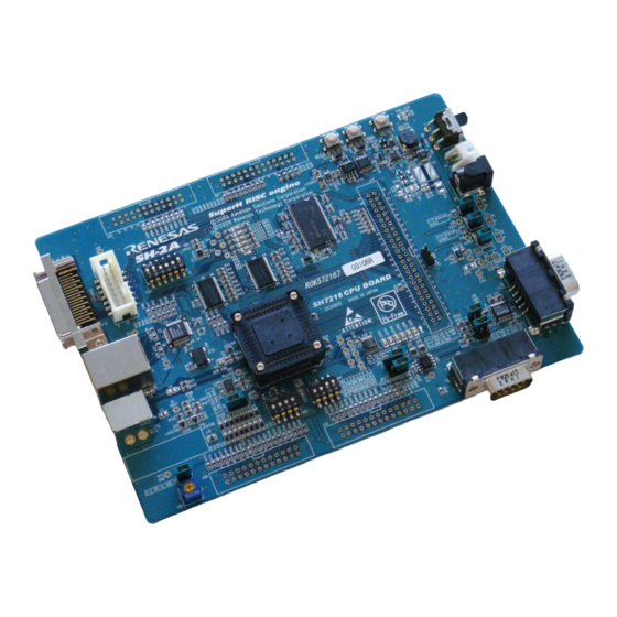
Overview 1.4 Exterior 1.4 Exterior The following figure shows the exterior of the R0K572167. Figure 1.4.1 R0K572167 Exterior Rev. 0.02 Mar. 27, 2009 REJ11J0038-0002... -
Page 9: Block Diagram
Overview 1.5 Block Diagram 1.5 Block Diagram The following figure shows the block diagram of the R0K572167. RCAN port H-UDI port connector H-UDI port connector Serial port USB port connector (36-pin) (14-pin) connector connector H-UDI SCI1 RCAN USBEXTAL (48.0 MHz) -
Page 10: Component Layout
Overview 1.6 Component Layout 1.6 Component Layout Figure 1.6.1 and Figure 1.6.2 show the layout of major components on the R0K572167. Figure 1.6.1 R0K572167 Component Layout (Top View of the Component Side) Rev. 0.02 Mar. 27, 2009 REJ11J0038-0002... - Page 11 Overview 1.6 Component Layout Figure 1.6.2 R0K572167 Component Layout (Top View of the Solder Side) Rev. 0.02 Mar. 27, 2009 REJ11J0038-0002...
- Page 12 Overview 1.6 Component Layout The following table lists the major components on the R0K572167. Table 1.6.1 Major Components on the R0K572167 Recommended Optional Components Symbol Name Remarks (Manufacturer Name and Part Number) SH7216 (Renesas) SDRAM MT48LC8M16A2P-7E (Micron) RS-232C driver SP3232ECA-L (Sipex)
-
Page 13: Memory Maps
Overview 1.7 Memory Map 1.7 Memory Maps Figure 1.7.1 and Figure 1.7.2 show memory map examples of the SH7216 and R0K572167. SH7216 Logic Space in MCU Mode 3 (Single-chip Mode) R0K572167 Memory Map H'0000 0000 H'0000 0000 Internal ROM (1024 KB) - Page 14 Overview 1.7 Memory Map SH7216 Logic Space in MCU Mode 2 (Internal ROM Enabled Mode) R0K572167 Memory Map H'0000 0000 H'0000 0000 Internal ROM (1024 KB) Internal ROM (1024 KB) H'000F FFFF H'000F FFFF H'0010 0000 H'0010 0000 Reserved Reserved...
-
Page 15: Absolute Maximum Ratings
Overview 1.8 Absolute Maximum Ratings 1.8 Absolute Maximum Ratings The following table lists the absolute maximum ratings of the R0K572167. Table 1.8.1 R0K572167 Absolute Maximum Ratings Symbol Parameter Value Remarks 5VCC 5 V system power supply voltage -0.3 to 6.0 V... - Page 16 Overview 1.9 Operating Conditions This page intentionally left blank. Rev. 0.02 Mar. 27, 2009 1-12 REJ11J0038-0002...
-
Page 17: Chapter 2Functions
Chapter 2Functions Chapter 2 Functions... -
Page 18: Overview Of Functions
Functions 2.1 Overview of Functions 2.1 Overview of Functions The R0K572167 includes the function modules listed in the following table. Table 2.1.1 R0K572167 Function Modules Section Function Description SH7216 • Input (XIN) clock: 12.5 MHz • CPU clock: 200 MHz max. -
Page 19: Cpu
2.2 CPU The R0K572167 includes the SH7216, the 32-bit RISC MCU that operates with a maximum frequency of 200 MHz. The SH7216 has 1024 KB of flash memory, 32 KB of EEPROM, and 128 KB of RAM to support various applications such as data processing and equipment control. -
Page 20: External Memory
Functions 2.3 External Memory 2.3 External Memory 2.3.1 SDRAM The R0K572167 includes 16 MB of SDRAM. The SH7216 on-chip bus state controller (BSC) controls the SDRAM. The following table lists the SDRAM specifications. Table 2.3.1 SDRAM Specifications Item Specification Configuration... -
Page 21: Serial Port Interface
2.4 Serial Port Interface On the R0K572167, SH7216 SCI channel 1 is connected to the serial port connector via the RS-232C transceiver. Also, SH7216 SCI channel 1 can be connected to the expansion connector (JA6), and the expansion connector can be connected to the serial port connector via the RS-232C transceiver. -
Page 22: I/O Ports
2.5 I/O Ports 2.5 I/O Ports SH7216 I/O ports are connected to the expansion connector on the R0K572167. Some I/O ports are also connected to DIP switches and LEDs, and can be used at the user’s discretion. The following figure shows the connection diagram of the LEDs and DIP switches. - Page 23 Functions 2.5 I/O Ports Table 2.5.1 and Table 2.5.2 list the I/O port functions. Table 2.5.1 I/O Port Functions (1/2) SH7216 Expansion Connectors Remarks Pin name PE1/TIOC0B/TIOC4BS/TEND0/MDC TIOC0B/TIOC4BS PE2/TIOC0C/TIOC4CS/DREQ1/WOL TIOC0C/TIOC4CS PE3/TIOC0D/TIOC4DS/TEND1/COL TIOC0D/TIOC4DS PE4/TIOC1A/SCK3/POE8/IRQ4/CRS TIOC1A/SCK3 PE5/TIOC1B/TIOC3BS/TXD3/MDIO TIOC1B/TIOC3BS/TXD3 PE6/TIOC2A/TIOC3DS/RXD3 TIOC2A/TIOC3DS/RXD3 PA21/RD/CKE/BACK/POE3/IRQ5/SCK1/FRAME PA20/WRL-DQMLL/CASU/BREQ/POE4/IRQ6/TXD1/AH [23] IRQ6 PA19/WRH-DQMLU/RASU/WAIT/POE8/IRQ7/RXD1/BS...
- Page 24 Functions 2.5 I/O Ports Table 2.5.2 I/O Port Functions (2/2) SH7216 Expansion Connectors Remarks Pin name PD21/D21/IRQ5/TEND1/AUDCK/EXOUT [22] PDX21 PD22/D22/IRQ6/DREQ1/WOL PD30/D30/TIOC3CS/SSL3/RX_ER [15] [SSL3] [14] [SSL2] PD31/D31/TIOC3AS/SSL2/RX_DV PA12/IRQ0/TIC5U/CS0/SSL1/TX_CLK [13] [SSL1] PA11/IRQ1/TIC5V/CS1/TX_EN/CRx0/RXD0 PA10/IRQ2/TIC5W/CS2/MII_TXD0/CTx0/TXD0 PA9/IRQ3/TCLKD/CS3/MII_TXD1/SSL0/SCK0 [12] [SSL0] PA8/IRQ4/TCLKC/CS4/MII_TXD2/MISO/RXD1 [11] [MISO] PA7/IRQ5/TCLKB/CS5/MII_TXD3/MOSI/TXD1 [10] [MOSI] [20] [TX_ER][RSPCK] PA6/IRQ6/TCLKA/CS6/TX_ER/RSPCK/SCK1...
-
Page 25: Usb Interface
2.6 USB Interface The R0K572167 includes a USB port connector (Series-B receptacle). Use the SH7216 PUPD output pin (PB15) to control the USB line. Set the PUPD pin to a low level to disable the VBUS input and USD+ pull-up when delaying the connection notification (such as high-priority processing or initialization) to a USB host or hub. -
Page 26: Rcan Interface
2.7 RCAN Interface 2.7 RCAN Interface The R0K572167 includes an RCAN port connector (D-sub, 9-pin connector). The CTx0 and RTx0 pins are connected to the RCAN connector (J10) via the RCAN transceiver. These pins can be connected to the expansion connector (JA5) via the switch jumpers (JP5 and JP6). -
Page 27: Ethernet Interface
Functions 2.8 Ethernet Interface 2.8 Ethernet Interface The R0K572167 includes an Ethernet port connector (RJ-45 connector) with a built-in pulse transformer. The following figure shows the R0K572167 Ethernet interface block diagram. Figure 2.8.1 Ethernet Interface Block Diagram Rev. 0.02 Mar. 27, 2009... -
Page 28: Interrupt Switches
Functions 2.9 Interrupt Switches 2.9 Interrupt Switches The SH7216 NMI and IRQ6 pins are connected to the push-button switches on the R0K572167. The following figure shows the interrupt switch block diagram. Figure 2.9.1 Interrupt Switch Block Diagram Rev. 0.02 Mar. 27, 2009... -
Page 29: E10A-Usb Interface
/FEW pins are connected to the SW1-1 system setting DIP switch. Turn SW1-1 OFF to connect the R0K572167 to the E10A-USB emulator. If SW1-1 is ON, the R0K572167 cannot be debugged correctly. Do not use the AUD pin when using the Ethernet interface. -
Page 30: Power Supply Module
2.11 Power Supply Module A 5 V power supply is input to R0K572167, and the regulator on the R0K572167 generates 1.5 V and 3.3 V. As it is a step down DC-DC switching regulator, the desired voltage can be generated by changing the resistance value. The R0K572167 can use a 5 V DC output stabilized power supply via power connector J4 or J6. -
Page 31: Clock Module
2.12 Clock Module The R0K572167 clock module is composed of two blocks. One block connects a crystal unit to EXTAL and XTAL, and one block connects EXTAL to the expansion connector (JA2). As a default, a 12.5 MHz crystal unit is connected to EXTAL and XTAL. - Page 32 Functions 2.13 Reset Module This page intentionally left blank. Rev. 0.02 Mar. 27, 2009 2-16 REJ11J0038-0002...
-
Page 33: Chapter 3Operating Specifications
Chapter 3Operating Specifications Chapter 3 Operating Specifications... -
Page 34: Connectors
Operating Specifications 3.1 Connectors 3.1 Connectors Figure 3.1.1 and Figure 3.1.2 show the connector assignments for the R0K572167. Figure 3.1.1 R0K572167 Connector Assignments (Top View of the Component Side) Rev. 0.02 Mar. 27, 2009 REJ11J0038-0002... - Page 35 Operating Specifications 3.1 Connectors Figure 3.1.2 R0K572167 Connector Assignments (Top View of the Solder Side) Rev. 0.02 Mar. 27, 2009 REJ11J0038-0002...
-
Page 36: H-Udi Port Connectors (J2 And J3)
3.1.1 H-UDI Port Connectors (J2 and J3) 3.1.1 H-UDI Port Connectors (J2 and J3) The R0K572167 includes 36-pin (J2) and 14-pin (J3) H-UDI port connectors to connect the board to an E10A-USB emulator. The following figure shows the pin assignments for J2. - Page 37 Operating Specifications 3.1.1 H-UDI Port Connectors (J2 and J3) The following figure shows the pin assignments for J3. Top view of the component side Side view Note that the pin number assignments of this connector differ from those of the connector manufacturer. Pin assignments of this connector Pin assignments...
-
Page 38: Serial Port Connector (J7)
Operating Specifications 3.1.2 Serial Port Connector (J7) 3.1.2 Serial Port Connector (J7) The R0K572167 includes a serial port connector (J7). The figure below shows the pin assignments for the serial port connector. Top view of the Board edge component side... -
Page 39: Power Supply Connector (J4)
Operating Specifications 3.1.3 Power Supply Connector (J4) 3.1.3 Power Supply Connector (J4) The R0K572167 includes a power supply connector (J4). The following figure shows the pin assignments for J4. Top view of the component side Board edge Side view Board edge Figure 3.1.6 J4 Pin Assignments... -
Page 40: Sh7216 External Power Supply Connectors (J8, J9, J12, J13)
3.1.4 SH7216 External Power Supply Connectors (J8, J9, J12, J13) External power supply connectors for CPU power, USB power, and analog power can be mounted on the R0K572167. To supply power using these connectors, remove the receptacle of the external power supply jumpers (JP8, JP9, JP12, and JP13) to leave it open. - Page 41 Operating Specifications 3.1.4 SH7216 External Power Supply Connectors (J8, J9, J12, J13) The following table lists the pin descriptions for J13. Table 3.1.5 J13 Pin Descriptions Pin Number Signal Name CVCC The following table lists the pin descriptions for J12. Table 3.1.6 J12 Pin Descriptions Pin Number Signal Name...
-
Page 42: Dc Power Supply Jack (J6)
Operating Specifications 3.1.5 DC Power Supply Jack (J6) 3.1.5 DC Power Supply Jack (J6) The R0K572167 includes a DC power supply jack (J6). The following figure shows the pin assignments for J6. Figure 3.1.8 J6 Pin Assignments The table below lists the pin descriptions for J6. -
Page 43: Expansion Connectors (Ja1, Ja2, Ja3, Ja5, Ja6)
3.1.6 Expansion Connectors (JA1, JA2, JA3, JA5, JA6) 3.1.6 Expansion Connectors (JA1, JA2, JA3, JA5, JA6) The R0K572167 includes through-holes for mounting expansion connectors. The SH7216 I/O pins are connected to the through-holes. The standard MIL connector can be connected to the through-holes to connect the expansion board, and to monitor the SH7216 bus signals. - Page 44 Operating Specifications 3.1.6 Expansion Connectors (JA1, JA2, JA3, JA5, JA6) Figure 3.1.10 Expansion Connectors Pin Assignments (Top View of the Solder Side) Note: Pin assignments on the CPU board are based on the assumption that the expansion connectors are mounted on the component side.
- Page 45 Operating Specifications 3.1.6 Expansion Connectors (JA1, JA2, JA3, JA5, JA6) The following table lists the pin descriptions for JA1. Table 3.1.10 JA1 Pin Descriptions Pin Number Signal Name Other Connections 5VCC ― ― 3VCC ― ― AVCC ― AGND ― AVREF ―...
- Page 46 Operating Specifications 3.1.6 Expansion Connectors (JA1, JA2, JA3, JA5, JA6) The following table lists the pin descriptions for JA2. Table 3.1.11 JA2 Pin Descriptions Pin Number Signal Name Other Connections RESET# ― EXTAL ― NMIIN ― ― WDTOVF# ― TXD0 ―...
- Page 47 Operating Specifications 3.1.6 Expansion Connectors (JA1, JA2, JA3, JA5, JA6) The following table lists the pin descriptions for JA3. Table 3.1.12 JA3 Pin Descriptions Pin Number Signal Name Other Connections ― SDRAM SDRAM SDRAM SDRAM SDRAM SDRAM SDRAM SDRAM SDRAM SDRAM SDRAM SDRAM...
- Page 48 Operating Specifications 3.1.6 Expansion Connectors (JA1, JA2, JA3, JA5, JA6) The following table lists the pin descriptions for JA5. Table 3.1.13 JA5 Pin Descriptions Pin Number Signal Name Other Connections ― ― ― ― ― ― ― ― CTx0 U15-3 to RCAN transceiver CRx0 U17-3 to RCAN transceiver ―...
- Page 49 Operating Specifications 3.1.6 Expansion Connectors (JA1, JA2, JA3, JA5, JA6) The following table lists the pin descriptions for JA6. Table 3.1.14 JA6 Pin Descriptions Pin Number Signal Name Other Connections DREQ0 ― DACK ― TEND ― ― ― RS232TX ― RS232RX ―...
-
Page 50: Rcan Port Connector (J10)
Operating Specifications 3.1.7 RCAN Port Connector (J10) 3.1.7 RCAN Port Connector (J10) The R0K572167 supports RCAN transmission and reception. The following figure shows the pin assignments for J10. Figure 3.1.11 J10 Pin Assignments The following table lists the pin descriptions for J10. -
Page 51: Usb Port Connector (J5)
Operating Specifications 3.1.8 USB Port Connector (J5) 3.1.8 USB Port Connector (J5) The R0K572167 includes a USB port connector (Series-B receptacle). The following figure shows the pin assignments for J5. Top view of the component side Board edge Side view Board edge Figure 3.1.12 J5 Pin Assignments... -
Page 52: Lan Port Connector (J1)
Operating Specifications 3.1.9 LAN Port Connector (J1) 3.1.9 LAN Port Connector (J1) The R0K572167 includes a LAN port connector (J1). The following figure shows the pin assignment for J1. Figure 3.1.13 J1 Pin Assignment The following table lists the pin descriptions for J1. -
Page 53: Gnd Connector (J11)
Operating Specifications 3.1.10 GND Connector (J11) 3.1.10 GND Connector (J11) The R0K572167 includes the GND connector (J11). The following figure shows the pin assignments for J11. Figure 3.1.14 J11 Pin Assignments The following table lists the pin descriptions for J11. -
Page 54: Switches And Leds
3.2 Switches and LEDs 3.2 Switches and LEDs The R0K572167 includes switches, a potentiometer, and LEDs as operating components. For potentiometer accuracy, refer to the manual provided by the manufacturer. The following figure shows the assignments of the R0K572167 operating components. -
Page 55: Usb Boot Clock Switch Jumper (Jp1)
Uses the system clock as the USB boot clock Uses the USB clock as the USB boot clock (default setting) Note: Do not change the jumper settings while the R0K572167 is ON. Be sure to turn the power OFF before changing the settings. -
Page 56: External Power Supply Switch Jumpers (Jp7, Jp3, Jp8, Jp9)
Operating Specifications 3.2.2 External Power Supply Switch Jumpers (JP7, JP3, JP8, JP9) 3.2.2 External Power Supply Switch Jumpers (JP7, JP3, JP8, JP9) Set JP3, JP8, and JP9 to switch the source of the power supply voltage to the system power supply (3VCC), analog power supply (AVCC), and A/D reference power supply (AVREF). -
Page 57: Serial Port Switch Jumpers (Jp2 And Jp4)
Operating Specifications 3.2.3 Serial Port Switch Jumpers (JP2 and JP4) 3.2.3 Serial Port Switch Jumpers (JP2 and JP4) Set the serial port switch jumpers (JP2 and JP4) to change the destination connector of the RS-232C transceiver, which is connected to the serial power connector (J7). SCI channel 1 is connected to J7 as default. -
Page 58: Rcan Port Switch Jumpers (Jp5 And Jp6)
Operating Specifications 3.2.4 RCAN Port Switch Jumpers (JP5 and JP6) 3.2.4 RCAN Port Switch Jumpers (JP5 and JP6) Set the RCAN port switch jumpers (JP5, and JP6) to switch the SH7216 pins connected to the RCAN transceiver (U16). U16 is connected to the SH7216 PA1/CTx0 and PA0/CRx0 pins via the level shifter as default. When not using these pins via U16, set JP5 and JP6 to 2-3. -
Page 59: Switches And Leds
Operating Specifications 3.2.5 Switches and LEDs 3.2.5 Switches and LEDs The R0K572167 includes seven switches and 12 LEDs. The following table lists the switches mounted on the board. Table 3.2.5 Switches Function Remarks System setting DIP switches (4/package) Refer to Table 3.2.6 for functions. - Page 60 Operating Specifications 3.2.5 Switches and LEDs The following table lists the SW1 functions. Set the SH7216 operating mode using the FWE, MD0, and MD1 pins. _______________ ___________________ The FWE pin is multiplexed to the ASEBRK /ASEBRKAK signals. Turn OFF SW1-1 (FWE) before using the E10A-USB emulator.
- Page 61 Operating Specifications 3.2.5 Switches and LEDs The following table lists the PHY operating mode settings. Table 3.2.8 PHY Operating Mode Setting Setting Description SW2-1 ISOLATE is high ISOLATE ISOLATE is low SW2-2 RPTR is high RPTR RPTR is low SW2-3 SPEED is high SPEED SPEED is low...
-
Page 62: Jumper/Switch Setting When Using The Development Tools
Operating Specifications 3.2.6 Jumper/Switch Setting when Using the Development Tools 3.2.6 Jumper/Switch Setting when Using the Development Tools _____________________ ________________ As the SH7216 signals connected to the emulator (FWE/ASEBRKAK /ASEBRK , TDI, TDO pins) are multiplexed to the on-chip flash writing control pins, set the jumpers and switches as shown in the following table when using development tools such as the E10A-USB emulator or the Flash Development Toolkit (FDT). -
Page 63: Dimensions
Operating Specifications 3.3 Dimensions 3.3 Dimensions Figure 3.3.1 and Figure 3.3.2 show the CPU board dimensions. Figure 3.3.1 CPU Board Dimensions (Top View of the Component Side) Rev. 0.02 Mar. 27, 2009 3-31 REJ11J0038-0002... - Page 64 Operating Specifications 3.3 Dimensions Figure 3.3.2 CPU Board Dimensions (Transparent View of the Solder Side) Rev. 0.02 Mar. 27, 2009 3-32 REJ11J0038-0002...
- Page 65 Operating Specifications 3.3 Dimensions This page intentionally left blank. Rev. 0.02 Mar. 27, 2009 3-33 REJ11J0038-0002...
-
Page 66: Appendix
Appendix SCHEMATICS... - Page 67 SH7216 CPU Board R0K572167 SCHEMATICS Note: 5VCC = Digital 5V TITLE PAGE 3VCC = 3.3V INDEX 1.5VCC = Core Vcc AVCC = CPU Analog 5V SH7216 AVREF = CPU Analog 5V Reference SDRAM-Ether/AUD,H-UDI,Reset VccQ = CPU/etc. 3.3V USB/SERIAL/RCAN/Power 3AVCC = Ether Analog 3.3V DrVCC = USB 3.3V...
- Page 68 0.001µFP 0.01µFP 0.01µFP 0.1µFP 0.1µFP PB7/A23/IRQ7/SCK4/TCLKC/TEND0 PB7/A23/IRQ7/SCK4/TCLKC/TEND0 PLLVSS PB8/A24/CS2/TCLKB/DREQ0/RXD4 PB8/A24/CS2/TCLKB/DREQ0/RXD4 PB9/A25/CS3/TCLKA/DACK0/TXD4 PB9/A25/CS3/TCLKA/DACK0/TXD4 :not mounted R0K572167 R0K572167 R0K572167 RENESAS SOLUTIONS CORPORATION RENESAS SOLUTIONS CORPORATION RENESAS SOLUTIONS CORPORATION Ver. 0.12 CPU_SH7216 CPU_SH7216 CPU_SH7216 DRAWN DRAWN DRAWN CHECKED CHECKED CHECKED DESIGNED DESIGNED DESIGNED...
- Page 69 CP46 2A10 2B10 0.1µFP 0.1µFP B3SN-3012 B3SN-3012 RESET# M51957BFP M51957BFP SN74CBTLV16210 SN74CBTLV16210 :not mounted R0K572167 R0K572167 R0K572167 RENESAS SOLUTIONS CORPORATION RENESAS SOLUTIONS CORPORATION RENESAS SOLUTIONS CORPORATION Ver. 0.12 SDRAM-Ether/AUD,H-UDI,Reset SDRAM-Ether/AUD,H-UDI,Reset SDRAM-Ether/AUD,H-UDI,Reset DRAWN DRAWN DRAWN CHECKED CHECKED CHECKED DESIGNED DESIGNED DESIGNED...
- Page 70 L300 L300 L300 XG8S-0231 XG8S-0231 CE13 CE13 0Ω 0Ω 10µF 10µF AVREFVSS :not mounted R0K572167 R0K572167 R0K572167 RENESAS SOLUTIONS CORPORATION RENESAS SOLUTIONS CORPORATION RENESAS SOLUTIONS CORPORATION Ver. 0.12 USB/SERIAL/RCAN/Power USB/SERIAL/RCAN/Power USB/SERIAL/RCAN/Power DRAWN DRAWN DRAWN CHECKED CHECKED CHECKED DESIGNED DESIGNED DESIGNED...
- Page 71 R223 R223 _100KΩ _100KΩ PA19 R224 R224 _100KΩ _100KΩ :not mounted R0K572167 R0K572167 R0K572167 RENESAS SOLUTIONS CORPORATION RENESAS SOLUTIONS CORPORATION RENESAS SOLUTIONS CORPORATION Ver. 0.12 Connectors,PUSH/DIP_SW,LED Connectors,PUSH/DIP_SW,LED Connectors,PUSH/DIP_SW,LED R224 (This Page) Remove (Double mount) DRAWN DRAWN DRAWN CHECKED CHECKED CHECKED...
- Page 72 Revision History SH7216 CPU board R0K572167 User's Manual Rev. Date of Issue Revisions page Summary 0.01 Feb. 20, 2009 ― First edition issued Modified module name from EEPROM to FLD. Updated the schematics in 0.02 Mar. 27, 2009 ― Appendix.
- Page 73 SH7216 CPU board R0K572167 User's Manual Publication Rev. 0.02 Date Mar. 27, 2009 Published by Renesas Technology Corp. Renesas Solutions Corp. © 2009. Renesas Technology Corp., All rights reserved. Printed in Japan.
- Page 74 R0K572167 User's Manual...
Need help?
Do you have a question about the R0K572167 and is the answer not in the manual?
Questions and answers