Table of Contents

Related Manuals for Aaeon HSB-910I


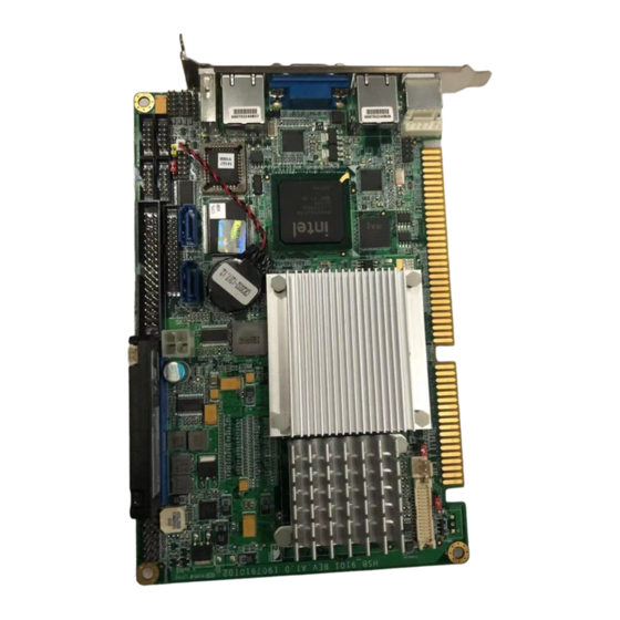
Summary of Contents for Aaeon HSB-910I
- Page 1 H a l f - s i z e S B C H S B - 9 1 0 I HSB-910I ® ® Intel Celeron M Processor ISA Expansion Half-size SBC Two 200-pin DDRII 400 SODIMM 2 SATA I/ 1 IDE/ 1 FDD/ 1 CompactFlash 5 USB 2.0/ 4 COM/ 1 IrDA...
-
Page 2: Copyright Notice
AAEON assumes no liabilities resulting from errors or omissions in this document, or from the use of the information contained herein. AAEON reserves the right to make changes in the product design without notice to its users. - Page 3 H a l f - s i z e S B C H S B - 9 1 0 I Acknowledgments All other products’ name or trademarks are properties of their respective owners. Award is a trademark of Award Software International, Inc. CompactFlash™...
-
Page 4: Packing List
H a l f - s i z e S B C H S B - 9 1 0 I Packing List Before you begin installing your card, please make sure that the following materials have been shipped: • 1 HSB-910I CPU Card • Floppy Cable • ATA100 Cable •... -
Page 5: Table Of Contents
H a l f - s i z e S B C H S B - 9 1 0 I Contents Chapter 1 General Information 1.1 Introduction..............1-2 1.2 Features ..............1-3 1.3 Specifications ............1-4 Chapter 2 Quick Installation Guide 2.1 Safety Precautions ............ - Page 6 H a l f - s i z e S B C H S B - 9 1 0 I 2.18 Digital I/O (CN1) ............2-12 2.19 LAN LED Connector (CN2, CN5)......2-13 2.20 Internal Keyboard Connector (CN3)......2-13 2.21 PS/2 Keyboard/ Mouse Connector (CN4)....2-13 2.22 Fan Connector (CN6) ..........
-
Page 7: Chapter 1 General Information
H a l f - s i z e S B C H S B - 9 1 0 I Chapter General Information 1- 1 Chapter 1 General Information... -
Page 8: Introduction
In addition to the comprehensive COM and USB offering the HSB-910I can also be configured with two or one (optional) Gigabit Ethernet ports to meet the needs of high bandwidth connectivity. Supporting CRT & LCD simultaneously along with the optional high definition audio board, the HSB-965P is an ideal solution for demanding multimedia based applications. -
Page 9: Features
H a l f - s i z e S B C H S B - 9 1 0 I 1.2 Features ® ® Intel Celeron M 90nm Processor Up to 1.8GHz ® ® Intel 910GMLE + Intel ICH6M 200-pin DDRII 400 SODIMM x 2, Up to 2GB Gigabit Ethernet x 2 or x 1 (Optional) ®... -
Page 10: Specifications
H a l f - s i z e S B C H S B - 9 1 0 I 1.3 Specifications System ® ® Intel Celeron M 90nm Processor up to 1.8GHz, FSB 400MHz (BGA/ Socket co-lay) System Memory Two DDRII SODIMM, support DDRII 400 up to 2GB ®... - Page 11 H a l f - s i z e S B C H S B - 9 1 0 I (Typical) CE/FCC Class A Display VGA Chipset Enhanced Integrated Graphics Memory Shared memory up to 256M Resolutions Up to 2048 x 1536 @ 32bpp for CRT;...
-
Page 12: Chapter 2 Quick Installation Guide
H a l f - s i z e S B C H S B - 9 1 0 I Chapter Quick Installation Guide Notice: The Quick Installation Guide is derived from Chapter 2 of user manual. For other chapters further installation instructions, please refer to the user... -
Page 13: Safety Precautions
H a l f - s i z e S B C H S B - 9 1 0 I 2.1 Safety Precautions Always completely disconnect the power cord from your board whenever you are working on it. Do not make connections while the power is on, because a sudden rush of power can damage sensitive electronic components. -
Page 14: Location Of Connectors And Jumpers
H a l f - s i z e S B C H S B - 9 1 0 I 2.2 Location of Connectors and Jumpers Component Side Solder Side 2 - 3 Chapter 2 Quick Installation Guide... -
Page 15: Mechanical Drawing
H a l f - s i z e S B C H S B - 9 1 0 I 2.3 Mechanical Drawing Component Side 2 - 4 Chapter 2 Quick Installation Guide... - Page 16 H a l f - s i z e S B C H S B - 9 1 0 I Solder Side 2 - 5 Chapter 2 Quick Installation Guide...
-
Page 17: List Of Jumpers
H a l f - s i z e S B C H S B - 9 1 0 I 2.4 List of Jumpers The board has a number of jumpers that allow you to configure your system to suit your application. The table below shows the function of each of the board's jumpers: Jumpers Label... -
Page 18: List Of Connectors
H a l f - s i z e S B C H S B - 9 1 0 I 2.5 List of Connectors The board has a number of connectors that allow you to configure your system to suit your application. The table below shows the function of each board's connectors: Connectors Label... - Page 19 H a l f - s i z e S B C H S B - 9 1 0 I DIMM1、2 DDRII Memory Slot Digital I/O LAN1 Active LED Connector PS/2 Keyboard/Mouse Connector Internal Keyboard Connector LAN2 Active LED Connector 3-pin Fan Connector LVDS Channel Connector AC97 Connector...
-
Page 20: Setting Jumpers
H a l f - s i z e S B C H S B - 9 1 0 I 2.6 Setting Jumpers You configure your card to match the needs of your application by setting jumpers. A jumper is the simplest kind of electric switch. It consists of two metal pins and a small metal clip (often protected by a plastic cover) that slides over the pins to connect them. -
Page 21: Clear Cmos (Jp1)
H a l f - s i z e S B C H S B - 9 1 0 I 2.7 Clear CMOS (JP1) Function Protected (Default) Clear 2.8 CF Voltage Selection (JP2) Function +3.3V (Default) 2.9 LVDS Voltage Selection (JP4) Function +3.3V (Default) 2.10 Front Panel Connector (FP1) -
Page 22: Battery Connector (Bt1)
H a l f - s i z e S B C H S B - 9 1 0 I 2.12 Battery Connector (BT1) Signal Signal VBAT(+) GND(-) 2.13 RS-232 Serial Port Connector (COM1, COM3, COM4) Signal Signal N.C. 2.14 RS-232/422/485 Serial Port Connector (COM2) Signal Signal DCD (422TXD-/485DATA-) -
Page 23: Lpt Port Connector (Lpt1)
H a l f - s i z e S B C H S B - 9 1 0 I 2.16 LPT Port Connector (LPT1) Signal Signal #STROBE #AFD DATA0 #ERROR DATA1 #INIT DATA2 #SLIN DATA3 DATA4 DATA5 DATA6 DATA7 #ACK BUSY SELECT... -
Page 24: Lan Led Connector (Cn2, Cn5)
H a l f - s i z e S B C H S B - 9 1 0 I DIO1-7 DIO1-8 2.19 LAN LED Connector (CN2, CN5) Signal Signal Active_LED(-) Active_LED(+) 2.20 Internal Keyboard Connector (CN3) Signal KB_CLK KB_DATA N.C. -
Page 25: Lvds Channel Connector (Cn7)
H a l f - s i z e S B C H S B - 9 1 0 I 2.23 LVDS Channel Connector (CN7) Signal Signal BKLEN BKLCTL PPVCC CH1_CLK# CH1_CLK PPVCC CH1_TX0# CH1_TX0 CH1_TX1# CH1_TX1 CH1_TX2# CH1_TX2 N.C. N.C. - Page 26 H a l f - s i z e S B C H S B - 9 1 0 I Below Table for China RoHS Requirements 产品中有毒有害物质或元素名称及含量 AAEON Main Board/ Daughter Board/ Backplane 有毒有害物质或元素 部件名称 铅 汞 镉 六价铬 多溴联苯...
-
Page 27: Chapter 3 Award Bios Setup
H a l f - s i z e S B C H S B - 9 1 0 I Chapter Award BIOS Setup Chapter 3 Award BIOS Setup 3-1... -
Page 28: System Configuration Verification
3. The CMOS memory has lost power and the configuration information has been erased. The HSB-910I CMOS memory has an integral lithium battery backup for data retention. However, you will need to replace the complete unit when it finally runs down. - Page 29 H a l f - s i z e S B C H S B - 9 1 0 I 3.2 Award BIOS Setup Awards BIOS ROM has a built-in Setup program that allows users to modify the basic system configuration. This type of information is stored in battery-backed CMOS RAM so that it retains the Setup information when the power is turned off.
- Page 30 Save CMOS value changes to CMOS and exit setup. Exit Without Saving Abandon all CMOS value changes and exit setup. You can refer to the "AAEON BIOS Item Description.pdf" file in the CD for the meaning of each setting in this chapter. Chapter 3 Award BIOS Setup 3-4...
-
Page 31: Chapter 4 Driver Installation
H a l f - s i z e S B C H S B - 9 1 0 I Chapter Driver Installation Chapter 4 Driver Installation... - Page 32 H a l f - s i z e S B C H S B - 9 1 0 I The HSB-910I comes with a CD-ROM that contains all drivers your need. Follow the sequence below to install the drivers: Step 1 –...
- Page 33 H a l f - s i z e S B C H S B - 9 1 0 I 4.1 Installation: Insert the HSB-910I CD-ROM into the CD-ROM Drive. And install the drivers from Step 1 to Step 3 in order. Step 1 – Install INF Driver 1.
-
Page 34: Appendix A Programming The Watchdog Timer
H a l f - s i z e S B C H S B - 9 1 0 I Appendix Programming the Watchdog Timer Appendix A Programming the Watchdog Timer... -
Page 35: Programming
H a l f - s i z e S B C H S B - 9 1 0 I A.1 Programming HSB-910I utilizes ITE 8712 chipset as its watchdog timer controller. ( K version ) Below are the procedures to complete its configuration and the AAEON intial watchdog timer program is also attached based on which you can develop customized program to fit your application. - Page 36 H a l f - s i z e S B C H S B - 9 1 0 I (1) Enter the MB PnP Mode To enter the MB PnP Mode, four special I/O write operations are to be performed during Wait for Key state. To ensure the initial state of the key-check logic, it is necessary to perform four write opera-tions to the Special Address port (2EH).
- Page 37 H a l f - s i z e S B C H S B - 9 1 0 I Description Reserved Returns to the Wait for Key state. This bit is used when the configuration sequence is completed. Resets all logical devices and restores configuration registers to their power-on states.
-
Page 38: Ite8712 Watchdog Timer Initial Program
H a l f - s i z e S B C H S B - 9 1 0 I WatchDog Timer Time-out Value (LSB) Register (Index=73h, Default=00h) Description WDT Time-out value 7-0 WatchDog Timer Time-out Value (MSB) Register (Index=74h, Default=00h) Description WDT Time-out value 15-8... - Page 39 H a l f - s i z e S B C H S B - 9 1 0 I mov cl, 73h call Superio_Set_Reg ;Clear by keyboard or mouse interrupt mov al, 0f0h mov cl, 71h call Superio_Set_Reg ;unit is second. mov al, 0C0H mov cl, 72h call Superio_Set_Reg...
- Page 40 H a l f - s i z e S B C H S B - 9 1 0 I MOV AL,BYTE PTR CS:[SI] OUT DX,AL INC SI LOOP Init_1 Enter_Configuration_Mode ENDP Exit_Configuration_Mode PROC NEAR MOV AX,0202h CALL Write_Configuration_Data Exit_Configuration_Mode ENDP Check_Chip PROC NEAR MOV AL,20h CALL Read_Configuration_Data...
- Page 41 H a l f - s i z e S B C H S B - 9 1 0 I Need_Initial: Not_Initial: Check_Chip ENDP Read_Configuration_Data PROC NEAR MOV DX,WORD PTR CS:[Cfg_Port+04h] OUT DX,AL MOV DX,WORD PTR CS:[Cfg_Port+06h] IN AL,DX Read_Configuration_Data ENDP Write_Configuration_Data PROC NEAR MOV DX,WORD PTR CS:[Cfg_Port+04h] OUT DX,AL...
- Page 42 H a l f - s i z e S B C H S B - 9 1 0 I push ax MOV DX,WORD PTR CS:[Cfg_Port+04h] mov al,cl out dx,al pop ax inc dx out dx,al Superio_Set_Reg endp.Set_Logic_Device proc near Set_Logic_Device proc near push ax push cx...
- Page 43 H a l f - s i z e S B C H S B - 9 1 0 I END Main Note: Interrupt level mapping 0Fh-Dh: not valid 0Ch: IRQ12 03h: IRQ3 02h: not valid 01h: IRQ1 00h: no interrupt selected A-10 Appendix A Programming the Watchdog Timer...
-
Page 44: Appendix B I/O Information
H a l f - s i z e S B C H S B - 9 1 0 I Appendix I/O Information Appendix B I/O Information... -
Page 45: I/O Address Map
H a l f - s i z e S B C H S B - 9 1 0 I B.1 I/O Address Map Appendix B I/O Information... -
Page 46: Memory Address Map
H a l f - s i z e S B C H S B - 9 1 0 I B.2 Memory Address Map Appendix B I/O Information... -
Page 47: Irq Mapping Chart
H a l f - s i z e S B C H S B - 9 1 0 I B.3 IRQ Mapping Chart B.4 DMA Channel Assignments Appendix B I/O Information... -
Page 48: Appendix C Mating Connector
H a l f - s i z e S B C H S B - 9 1 0 I Appendi Mating Connector C - 1 Appendix C Mating Connector... -
Page 49: List Of Mating Connectors And Cables
H a l f - s i z e S B C H S B - 9 1 0 I C.1 List of Mating Connectors and Cables The table notes mating connectors and available cables. Connector Function Mating Connector Available Cable P/N Label Cable... - Page 50 H a l f - s i z e S B C H S B - 9 1 0 I VGA1 Catch 3125-000-15S Display Electronics Connector IrDA JIH VEI 21B12050-XX Connector Electronics S10B-01G-4/2 Digital I/O JIH VEI Electronics LAN 1 JIH VEI Active LED Electronics...
Need help?
Do you have a question about the HSB-910I and is the answer not in the manual?
Questions and answers