Table of Contents
Advertisement
Quick Links
Advertisement
Table of Contents

Subscribe to Our Youtube Channel
Related Manuals for Aaeon HSB-LN2I


Summary of Contents for Aaeon HSB-LN2I
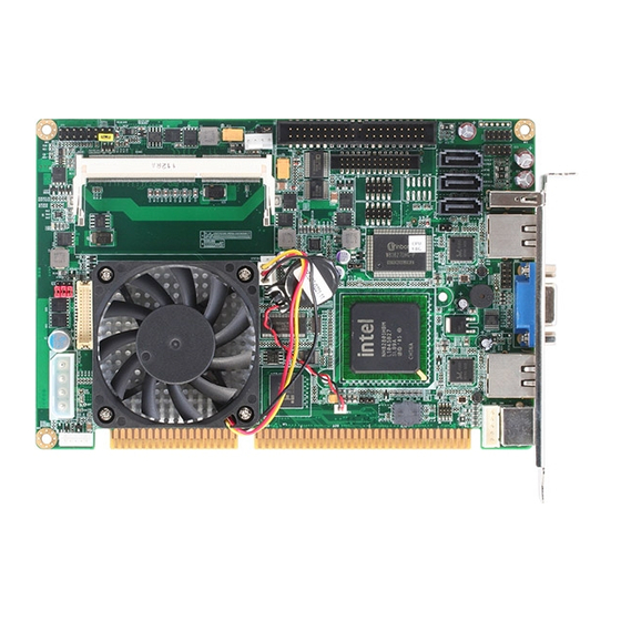
- Page 1 H S B - L N 2 I HSB-LN2I ® Intel Atom™ D525/N455 Processor ISA Expansion Half-size SBC Two 204-pin DDR3 667/800 SODIMM 3 SATA 3.0 Gb/s/ 1 IDE/ 1 CompactFlash™ 5 USB2.0/ 2 COM/ 1 VGA/ 1 LVDS HSB-LN2I Manual 2nd Ed. September 18, 2014...
- Page 2 AAEON assumes no liabilities resulting from errors or omissions in this document, or from the use of the information contained herein. AAEON reserves the right to make changes in the product design without notice to its users.
- Page 3 H a l f - s i z e S B C H S B - L N 2 I Acknowledgments All other products’ name or trademarks are properties of their respective owners. AMI is a trademark of American Megatrends Inc. ...
- Page 4 1 Serial Cable 3 SATA Cables 1 Product CD (manual in PDF format and drivers) 1 HSB-LN2I CPU Card If any of these items should be missing or damaged, please contact your distributor or sales representative immediately.
-
Page 5: Table Of Contents
H a l f - s i z e S B C H S B - L N 2 I Contents Chapter 1 General Information 1.1 Introduction ..............1-2 1.2 Features ..............1-3 1.3 Specification .............. 1-4 Chapter 2 Quick Installation Guide 2.1 Safety Precautions ............ - Page 6 H a l f - s i z e S B C H S B - L N 2 I 2.18 Caseopen Pin Header(CN1) ........2-16 2.19 HD Audio Codec with Realtek ALC888 (Optional) Connector (CN2) ............. 2-16 2.20 LVDS Connector (CN3) ........... 2-17 2.21 PS2 Keyboard/Mouse Connector (CN4) ....
- Page 7 H a l f - s i z e S B C H S B - L N 2 I Chapter 3 AMI BIOS Setup 3.1 System Test and Initialization........3-2 3.2 AMI BIOS Setup ............3-3 Chapter 4 Driver Installation 4.1 Installation ..............
-
Page 8: Chapter 1 General Information
H a l f - s i z e S B C H S B - L N 2 I Chapter General Information 1- 1 Chapter 1 General Information... -
Page 9: Introduction
In addition to the comprehensive COM and USB offering the HSB-LN2I can also be configured with two Gigabit Ethernet ports to meet the needs of high bandwidth connectivity. Supporting CRT & LCD simultaneously along with the optional high definition audio board, the HSB-LN2I is an ideal solution for demanding multimedia based applications. -
Page 10: Features
USB2.0 x 5, RS-232/422/485 x 1, RS-232 x 1, Parallel x 1 ISA Expansion +5V, +12V Operation, AT Power Note: HSB-LN2I has to be operated with an ISA backplane to supply +5V, +12V, and -12V power inputs to make COM1 work functionally. 1- 3 Chapter 1 General Information... -
Page 11: Specification
H a l f - s i z e S B C H S B - L N 2 I 1.3 Specification System Form Factor ISA Half-size Board ® Onboard Intel Atom™ D525 Processor up to 1.8GHz with a 1 MB L2 cache;... - Page 12 Power Requirement 4-pin power connector (+5V, +12V) Note: HSB-LN2I has to be operated with an ISA backplane. Normally, onboard 4-pin power connector can supply power (+5V and +12V) to operate the board. But the COM1 will need +5V and ±12V power supplied through the ISA bus.
- Page 13 H a l f - s i z e S B C H S B - L N 2 I integrated Graphics Core Resolutions D525: Up to 2048x1536 @ 60Hz for CRT; 1366x768 @ 60Hz for N455: Up to 1400x1050 @ 60Hz for CRT;...
-
Page 14: Chapter 2 Quick Installation Guide
H a l f - S i z e S B C H S B - L N 2 I Chapter Quick Installation Guide Chapter 2 Quick Installation Guide... -
Page 15: Safety Precautions
H a l f - S i z e S B C H S B - L N 2 I 2.1 Safety Precautions Always completely disconnect the power cord from your board whenever you are working on it. Do not make connections while the power is on, because a sudden rush of power can damage sensitive electronic components. -
Page 16: Location Of Connectors And Jumpers
H a l f - S i z e S B C H S B - L N 2 I 2.2 Location of Connectors and Jumpers Component Side Chapter 2 Quick Installation Guide... - Page 17 H a l f - S i z e S B C H S B - L N 2 I Solder Side Chapter 2 Quick Installation Guide...
-
Page 18: Mechanical Drawing
H a l f - S i z e S B C H S B - L N 2 I 2.3 Mechanical Drawing Component Side Chapter 2 Quick Installation Guide... - Page 19 H a l f - S i z e S B C H S B - L N 2 I Solder Side Chapter 2 Quick Installation Guide...
-
Page 20: List Of Jumpers
H a l f - S i z e S B C H S B - L N 2 I 2.4 List of Jumpers The board has a number of jumpers that allow you to configure your system to suit your application. The table below shows the function of each of the board's jumpers: Label Function... -
Page 21: List Of Connectors
H a l f - S i z e S B C H S B - L N 2 I 2.5 List of Connectors The board has a number of connectors that allow you to configure your system to suit your application. The table below shows the function of each board's connectors: Label Function... - Page 22 H a l f - S i z e S B C H S B - L N 2 I SYS_FAN1 4-Pin System Fan Connector PCIE_12V1 4-Pin ATX Power Connector Battery Connector SATA1 SATA Connector SATA2 SATA Connector SATA3 SATA Connector SPI1 BIOS DEBUG PORT IDE1...
-
Page 23: Setting Jumpers
H a l f - S i z e S B C H S B - L N 2 I 2.6 Setting Jumpers You configure your card to match the needs of your application by setting jumpers. A jumper is the simplest kind of electric switch. It consists of two metal pins and a small metal clip (often protected by a plastic cover) that slides over the pins to connect them. -
Page 24: Cf Selection (Jp1)
H a l f - S i z e S B C H S B - L N 2 I 2.7 CF Selection (JP1) Master Slave Function Master (Default) Slave 2.8 LCD Panel Voltage Selection (JP2) +3.3V (Default) Function +3.3V(Default) 2.9 LCD Backlight Voltage Selection (JP3) PWM Mode Bias Mode (Default) -
Page 25: Lcd Backlight Inverter Vcc Selection (Jp3)
H a l f - S i z e S B C H S B - L N 2 I 2.10 LCD Backlight Inverter VCC Selection (JP3) +12V (Default) Function +12V (Default) 2.11 Clear CMOS (JP4) Normal (Default) Clear CMOS Function Normal (Default) Clear CMOS... -
Page 26: Front Panel Connector (Fp1)
H a l f - S i z e S B C H S B - L N 2 I 2.13 Front Panel Connector (FP1) Signal PWR_BTN+ H/W RESET+ PWR_BTN- H/W RESET- HDD_LED+ PWR_LED+ HDD_LED- PWR_LED- 2.14 Front Panel Connector (FP2) Signal External Speaker (+) Key Board Lock (+) -
Page 27: Vga Connector (Vga1)
H a l f - S i z e S B C H S B - L N 2 I Internal Buzzer (-) I2C Bus SMB Clock External Speaker (-) I2C Bus SMB Data 2.15 VGA Connector (VGA1) Pin Name Signal Type Signal Level GREEN... -
Page 28: Serial Connector (Com1)
H a l f - S i z e S B C H S B - L N 2 I DDC_CLK 2.16 RS-232 Serial Connector (COM1) Pin Name Signal Type Signal Level ±9V ±9V ±9V RI/+5V/+12V IN/ PWR +5V/+12V 2.17 RS-232/485/422 Serial Connector (COM2) Pin Name Signal Type Signal Level... -
Page 29: Caseopen Pin Header(Cn1)
H a l f - S i z e S B C H S B - L N 2 I RXD (422RXD+) TXD(422TXD+/485DATA+) ±9V DTR(422RXD-) ±9V ±9V RI/+5V/+12V IN/ PWR +5V/+12V 2.18 Caseopen Pin Header(CN1) Pin Name Signal Type Signal Level CASEOPEN# 2.19 HD Audio Codec with Realtek ALC888 (Optional) Connector (CN2) -
Page 30: Lvds Connector (Cn3)
H a l f - S i z e S B C H S B - L N 2 I Pin Name Signal Type Signal Level SYNC SDIN SDOUT +3.3V BCLK +3.3V +3.3V 2.20 LVDS Connector (CN3) Pin Name Signal Type Signal Level BKL_ENABLE BKL_CONTROL... - Page 31 H a l f - S i z e S B C H S B - L N 2 I LVDS_A_CLK- DIFF LVDS_A_CLK+ DIFF LCD_PWR +3.3V/+5V LVDS_DA0- DIFF LVDS_DA0+ DIFF LVDS_DA1- DIFF LVDS_DA1+ DIFF LVDS_DA2- DIFF LVDS_DA2+ DIFF LVDS_DA3- DIFF LVDS_DA3+ DIFF DDC_DATA...
-
Page 32: Ps2 Keyboard/Mouse Connector (Cn4)
H a l f - S i z e S B C H S B - L N 2 I LVDS_B_CLK- DIFF LVDS_B_CLK+ DIFF Note: LVDS LCD_PWR can be set to +3.3V or +5V by JP2. 2.21 PS2 Keyboard/Mouse Connector (CN4) Pin Name Signal Type Signal Level... -
Page 33: Lvds Inverter/ Backlight Connector (Cn6)
H a l f - S i z e S B C H S B - L N 2 I KBDATA 2.23 LVDS Inverter/ Backlight Connector (CN6) Pin Name Signal Type Signal Level BKL_PWR +5V / +12V BKL_CONTROL BKL_ENABLE Note: LVDS1 BKL_PWR can be set to +5V or +12V by JP3. LVDS1 BKL_CONTROL can be set by JP3. -
Page 34: Realtek Lan (Rj-45) Port (Lan2)
H a l f - S i z e S B C H S B - L N 2 I Pin Name Signal Type Signal Level MDI0+ DIFF MDI0- DIFF MDI1+ DIFF MDI2+ DIFF MDI2- DIFF MDI1- DIFF MDI3+ DIFF MDI3- DIFF 2.25 Realtek LAN (RJ-45) Port (LAN2) -
Page 35: Ddr3 Sodimm Slot (Dimm1)
H a l f - S i z e S B C H S B - L N 2 I 2.26 DDR3 SODIMM Slot (DIMM1) Standard specification 2.27 DDR3 SODIMM Slot (DIMM2) Standard specification 2.28 USB2.0 Port 4 and Port 5 (USB1) Pin Name Signal Type Signal Level... -
Page 36: Usb2.0 Port 2 And Port 3 (Usb2)
H a l f - S i z e S B C H S B - L N 2 I 2.29 USB2.0 Port 2 and Port 3 (USB2) Pin Name Signal Type Signal Level +5VSB USB2_D- DIFF USB2_D+ DIFF USB3_D+ DIFF USB3_D- DIFF... -
Page 37: 4-Pin Cpu Fan Connector (Cpu_Fan1)
H a l f - S i z e S B C H S B - L N 2 I USB2_D- DIFF USB2_D+ DIFF 2.31 4-Pin CPU Fan Connector (CPU_FAN1) Pin Name Signal Type Signal Level +12V SENSE CTRL 2.32 4-Pin SYS Fan Connector (SYS_FAN1) Pin Name Signal Type Signal Level... -
Page 38: 4-Pin Atx Power Connector (Pcie_12V1)
H a l f - S i z e S B C H S B - L N 2 I 2.33 4-Pin ATX Power Connector (PCIE_12V1) Pin Name Signal Type Signal Level +12V +12V +5V_ATX 2.34 Battery Connector (BT1) Pin Name Signal Type Signal Level VBAT... -
Page 39: Sata Port 1 (Sata2)
H a l f - S i z e S B C H S B - L N 2 I SATA_TX0+ DIFF SATA_TX0- DIFF SATA_RX0- DIFF SATA_RX0+ DIFF 2.36 SATA Port 1 (SATA2) Pin Name Signal Type Signal Level SATA_TX1+ DIFF SATA_TX1- DIFF... -
Page 40: Bios Debug Port (Spi1)
H a l f - S i z e S B C H S B - L N 2 I Pin Name Signal Type Signal Level SATA_TX2+ DIFF SATA_TX2- DIFF SATA_RX2- DIFF SATA_RX2+ DIFF 2.38 BIOS DEBUG PORT (SPI1) Pin Name Signal Type Signal Level +3.3V_SPI... -
Page 41: Ide Connector (Ide1)
H a l f - S i z e S B C H S B - L N 2 I 2.39 IDE Connector (IDE1) Pin Name Signal Type Signal Level /RESET Data 7 Data 8 Data 6 Data 9 Data 5 Data 10 Data 4 Data 11... - Page 42 H a l f - S i z e S B C H S B - L N 2 I DMA Request Write Strobe Read Strobe I/O Ready Spindle Sync or Cable Select DMA Acknowledge Interrupt Request Address 1 Passed Diagnostics Address 0 Address 2 /IDE_CS0...
-
Page 43: Parallel Port Connector (Lpt1)
H a l f - S i z e S B C H S B - L N 2 I 2.40 Parallel Port Connector (LPT1) Pin Name Signal Type Signal Level STROBE# AFD# ERROR# PRINT# SLIN# 2-30 Chapter 2 Quick Installation Guide... - Page 44 H a l f - S i z e S B C H S B - L N 2 I ACK# BUSY SLCT 2-31 Chapter 2 Quick Installation Guide...
- Page 45 H a l f - S i z e S B C H S B - L N 2 I Below Table for China RoHS Requirements 产品中有毒有害物质或元素名称及含量 AAEON Main Board/ Daughter Board/ Backplane 有毒有害物质或元素 部件名称 铅 汞 镉 六价铬 多溴联苯...
- Page 46 H a l f - s i z e S B C H S B - L N 2 I Chapter BIOS Setup Chapter 3 AMI BIOS Setup 3-1...
-
Page 47: System Test And Initialization
3. The CMOS memory has lost power and the configuration information has been erased. The HSB-LN2I CMOS memory has an integral lithium battery backup for data retention. However, you will need to replace the complete unit when it finally runs down. -
Page 48: Ami Bios Setup
H a l f - s i z e S B C H S B - L N 2 I 3.2 AMI BIOS Setup AMI BIOS ROM has a built-in Setup program that allows users to modify the basic system configuration. This type of information is stored in battery-backed CMOS RAM so that it retains the Setup information when the power is turned off. - Page 49 H a l f - s i z e S B C H S B - L N 2 I Setup submenu: Main Chapter 3 AMI BIOS Setup 3-4...
- Page 50 H a l f - s i z e S B C H S B - L N 2 I Setup submenu: Advanced Chapter 3 AMI BIOS Setup 3-5...
- Page 51 H a l f - s i z e S B C H S B - L N 2 I ACPI Settings Options Summary : ACPI Sleep State S1 Only (CPU Stop Clock) S3 Only (Suspend to RAM) S1 & S3 (Auto) Default Select ACPI sleep state the system will enter when the SUSPEND button is pressed.
- Page 52 H a l f - s i z e S B C H S B - L N 2 I CPU Configuration Options Summary : Hyper-Threading Disabled Enabled Default Enabled for Windows XP and Linux (OS optimized for Hyper-Threading Technology) and Disabled for other OS (OS not optimized for Hyper-Threading Technology).
- Page 53 H a l f - s i z e S B C H S B - L N 2 I SATA Configuration (IDE) Chapter 3 AMI BIOS Setup 3-8...
- Page 54 H a l f - s i z e S B C H S B - L N 2 I SATA Configuration (AHCI) Options summary : SATA Controller(s) Enabled Default Disabled Enable or disable SATA device. SATA Mode Selection Default AHCI Determines how SATA controller(s) operate.
- Page 55 H a l f - s i z e S B C H S B - L N 2 I USB Configuration Options summary : Legacy USB Support Enabled Default Disabled Auto Enable Legacy USB support. Auto option disables legacy support if no USB devices are connected.
- Page 56 H a l f - s i z e S B C H S B - L N 2 I W83627DHG Super IO Configuration Options Summary : Serial Port 1 Set Parameters of Serial Port 1 (COMA) Configuration Serial Port 2 Set Parameters of Serial Port 2 (COMB) Configuration Parallel Port...
- Page 57 H a l f - s i z e S B C H S B - L N 2 I -Serial Port 1 Configuration Options Summary : Serial Port Disabled Enabled Default Enable or Disable Serial Port (COM) Change Settings Auto Default IO=3F8h;...
- Page 58 H a l f - s i z e S B C H S B - L N 2 I -Serial Port 2 Configuration Options Summary : Serial Port Disabled Enabled Default Enable or Disable Serial Port (COM) Change Settings Auto Default IO=2F8h;...
- Page 59 H a l f - s i z e S B C H S B - L N 2 I RS232/422,485 RS232 Default RS422 RS485 RS232/422,485 switch -Parallel Port Configuration Options Summary : Parallel Port Disabled Enabled Default Enable or Disable Parallel Port (LPT/LPTE) Change Settings Auto Default...
- Page 60 H a l f - s i z e S B C H S B - L N 2 I IO=378h; IRQ=7 IO=378h; IRQ=5, 7 IO=278h; IRQ=5, 7 IO=3BCh; IRQ=5, 7 Select an optimal setting for Super IO device. Device Mode STD Printer Mode Default SPP Mode...
- Page 61 H a l f - s i z e S B C H S B - L N 2 I W83627DHG HW Monitor Options Summary : Smart Fan Function Disabled Enabled Default Enable or Disable Smart Fan Smart Fan Mode Smart Fan Mode Select Configuration Chapter 3 AMI BIOS Setup 3-16...
- Page 62 H a l f - s i z e S B C H S B - L N 2 I -Smart Fan Mode Configuration Options Summary : SYS Smart Fan Mode Manual Mode Default Thermal Cruise Mode Fan Speed Cruise Mode SYS Smart Fan Mode Select SYSFAN PWM/DC Voltage...
- Page 63 H a l f - s i z e S B C H S B - L N 2 I CPU Smart Fan 0 Mode Manual Mode Default Thermal Cruise Mode Fan Speed Cruise Mode SMART FAN III Mode CPU Smart Fan 0 Mode Select CPUFAN0 PWM/DC Voltage 0~255 Default : 255...
- Page 64 H a l f - s i z e S B C H S B - L N 2 I Dynamic Digital IO Configuration Options Summary : DIO0 Direction Input Default Output Set Digital IO as Input or Output DIO1 Direction Input Default Output...
- Page 65 H a l f - s i z e S B C H S B - L N 2 I DIO3 Direction Input Default Output Set Digital IO as Input or Output DIO4 Direction Input Output Default Set Digital IO as Input or Output DIO5 Direction Input Output...
- Page 66 H a l f - s i z e S B C H S B - L N 2 I Power Management Options Summary : Power Mode ATX Type Default AT Type Select power supply mode. AC Power Loss State Always OFF Always ON Last State...
- Page 67 H a l f - s i z e S B C H S B - L N 2 I For En/Disable Ring In wake up function. Attention please, when this function is enabled, some devices which connect to Serial Port may cause the system auto wake up from sleep mode.
- Page 68 H a l f - s i z e S B C H S B - L N 2 I Wake system with Dynamic Disabled Default Time Enabled Enable or disable System wake on alarm event. When enabled, System will wake on the hr::min::sec specified Chapter 3 AMI BIOS Setup 3-23...
- Page 69 H a l f - s i z e S B C H S B - L N 2 I Setup submenu: Chipset Options Summary : Host Bridge System Agent (SA) Parameters Sourth Bridge I/O Controller Hub Parameters Chapter 3 AMI BIOS Setup 3-24...
- Page 70 H a l f - s i z e S B C H S B - L N 2 I Host Bridge Options Summary : Intel IGD Configuration Configure Integrated Graphic Settings Chapter 3 AMI BIOS Setup 3-25...
- Page 71 H a l f - s i z e S B C H S B - L N 2 I -Intel IGD Configuration Options Summary : IGD – Boot Type VBIOS Default Default CRT + LFP Select the Video Device which will be activated during POST. LVDS Panel Type 640x480 800x600...
- Page 72 H a l f - s i z e S B C H S B - L N 2 I 1280x1024 1280x768 1366x768 1280x800 Select LCD panel used by Internal Graphics Device by selecting the appropriate setup item. LVDS Backlight Level 100% Default Select Backlight brightness of LVDS...
- Page 73 H a l f - s i z e S B C H S B - L N 2 I South Bridge Options Summary : HD Audio Controller Enabled Disabled Default For En/Disable HD Audio Controller. Chapter 3 AMI BIOS Setup 3-28...
- Page 74 H a l f - s i z e S B C H S B - L N 2 I Setup submenu: Boot Options summary : Quiet Boot Disabled Enabled Default Enables or disables Quiet Boot option Launch RTL8111E PXE Disabled Default OpROM...
- Page 75 H a l f - s i z e S B C H S B - L N 2 I Boot Option Priorities Options Summary : Boot Option #X Your device Your device Sets the system boot order Chapter 3 AMI BIOS Setup 3-30...
- Page 76 H a l f - s i z e S B C H S B - L N 2 I Setup submenu: Security Change User/Supervisor Password You can install a Supervisor password, and if you install a supervisor password, you can then install a user password. A user password does not provide access to many of the features in the Setup utility.
- Page 77 H a l f - s i z e S B C H S B - L N 2 I Setup utility. Removing the Password Highlight this item and type in the current password. At the next dialog box press Enter to disable password protection. Chapter 3 AMI BIOS Setup 3-32...
- Page 78 H a l f - s i z e S B C H S B - L N 2 I Setup submenu: Exit Chapter 3 AMI BIOS Setup 3-33...
-
Page 79: Chapter 4 Driver Installation
H a l f - s i z e S B C H S B - L N 2 I Chapter Driver Installation Chapter 4 Driver Installation... - Page 80 H a l f - s i z e S B C H S B - L N 2 I The HSB-LN2I comes with a CD-ROM that contains all drivers your need. Follow the sequence below to install the drivers: Step 1 –...
- Page 81 H a l f - s i z e S B C H S B - L N 2 I 4.1 Installation: Insert the HSB-LN2I CD-ROM into the CD-ROM Drive. And install the drivers from Step 1 to Step 5 in order. Step 1 – Install Chipset Driver 1.
- Page 82 H a l f - s i z e S B C H S B - L N 2 I Step 5 – Install Audio Driver 1. Click on the Step 5 - Audio folder and select the OS your system is 2.
-
Page 83: Appendix A Programming The Watchdog Timer
H a l f - s i z e S B C H S B - L N 2 I Appendix Programming the Watchdog Timer Appendix A Programming the Watchdog Timer... -
Page 84: Programming
HSB-LN2I utilizes W83627DHG-P chipset as its watchdog timer controller. Below are the procedures to complete its configuration and the AAEON intial watchdog timer program is also attached based on which you can develop customized program to fit your application. Configuring Sequence Description... - Page 85 H a l f - s i z e S B C H S B - L N 2 I (3) Exit the W83627DHG config Mode. Undesired result may occur if the config Mode is not exited normally. (1) Enter the W83627DHG config Mode To enter the W83627DHG config Mode, two special I/O write operations are to be performed during Wait for Key state.
- Page 86 H a l f - s i z e S B C H S B - L N 2 I = 010 Power LED pin is driven low. = 011 Power LED pin outputs 2Hz pulse with 50% duty cycle. = 100 Power LED pin outputs 1Hz pulse with 50% duty cycle.
- Page 87 H a l f - s i z e S B C H S B - L N 2 I WatchDog Timer Register II (Index=F6h, Default=00h) Bit 7-0 = 0 x 00 Time-out Disable = 0 x 01 Time-out occurs after 1 second/minute = 0 x 02 Time-out occurs after 2 second/minutes...
- Page 88 H a l f - s i z e S B C H S B - L N 2 I Force Watchdog Timer time-out event: this bit is self-clearing Bit 4 : Watchdog Timer Status. R/W Watchdog Timer time-out occurred Watchdog Timer counting Bit 3-0 : These bits select IRQ resource for...
-
Page 89: W83627Dhg Watchdog Timer Initial Program
H a l f - s i z e S B C H S B - L N 2 I A.2 W83627DHG Watchdog Timer Initial Program Example: Setting 10 sec. as Watchdog timeout interval ;/////////////////////////////////////////////////////////////////////////////////////////////// Mov dx,2eh ;Enter W83627DHG config mode Mov al,87h (out 87h to 2eh twice) Out dx,al... - Page 90 H a l f - s i z e S B C H S B - L N 2 I ;/////////////////////////////////////////////////////////////////////////////////////////////// Dec dx Mov al,0f5h ;CRF5 (PLED mode register) Out dx,al Inc dx In al,dx And al,not 08h ;Set second as counting unit Out dx,al ;/////////////////////////////////////////////////////////////////////////////////////////////// Dec dx...
-
Page 91: Appendix B I/O Information
H a l f - s i z e S B C H S B - L N 2 I Appendix I/O Information Appendix B I/O Information... -
Page 92: I/O Address Map
H a l f - s i z e S B C H S B - L N 2 I B.1 I/O Address Map Appendix B I/O Information... -
Page 93: Memory Address Map
H a l f - s i z e S B C H S B - L N 2 I B.2 Memory Address Map Appendix B I/O Information... -
Page 94: Irq Mapping Chart
H a l f - s i z e S B C H S B - L N 2 I B.3 IRQ Mapping Chart Appendix B I/O Information... - Page 95 H a l f - s i z e S B C H S B - L N 2 I Appendix B I/O Information...
-
Page 96: Dma Channel Assignments
H a l f - s i z e S B C H S B - L N 2 I B.4 DMA Channel Assignments Appendix B I/O Information... -
Page 97: Appendix C Mating Connector
H a l f - s i z e S B C H S B - L N 2 I Appendix Mating Connector C - 1 Appendix C Mating Connector... -
Page 98: List Of Mating Connectors And Cables
H a l f - s i z e S B C H S B - L N 2 I C.1 List of Mating Connectors and Cables The table notes mating connectors and available cables. Connector Function Mating Connector Available Cable P/N Label Cable... - Page 99 H a l f - s i z e S B C H S B - L N 2 I CFD1 CF Card Comweal 60328226 Connector Front JIH VEI 21B22564-XX Panel Electronics S10B-01G-6/3 Connector -VXX Front JIH VEI 21B22564-XX Panel Electronics S10B-01G-6/3 Connector...
-
Page 100: Appendix D Ahci Setting
H a l f - s i z e S B C H S B - L N 2 I Appendix AHCI Setting Appendix D AHCI Setting... -
Page 101: Setting Ahci
H a l f - s i z e S B C H S B - L N 2 I D.1 Setting AHCI OS installation to setup AHCI Mode Step 1: Copy the files below from “Driver CD -> Step 4 - AHCI-> winxp_32 or winxp_64 to Disk Step 2: Connect the USB Floppy (disk with AHCI files) to the board Appendix D AHCI Setting... - Page 102 H a l f - s i z e S B C H S B - L N 2 I Step 3: The setting procedures “ In BIOS Setup Menu” A: Advanced -> IDE Configuration -> ATA Or IDE Configuration -> Enhanced B: Configure SATA As ->...
- Page 103 H a l f - s i z e S B C H S B - L N 2 I Step 5: The setting procedures “In BIOS Setup Menu” C: Save & Exit -> Save Changes and Exit Step 6: Setup OS Appendix D AHCI Setting...
- Page 104 H a l f - s i z e S B C H S B - L N 2 I Step 7: Press “F6” Step 8: Choose “S” Appendix D AHCI Setting...
- Page 105 H a l f - s i z e S B C H S B - L N 2 I Step 9: Choose “Intel(R) ICH8-M-E/M SATA AHCI Controller” Step 10: It will show the model number you select and then press “ENTER” Appendix D AHCI Setting...
- Page 106 H a l f - s i z e S B C H S B - L N 2 I Step 11: Setup is loading files Appendix D AHCI Setting...
Need help?
Do you have a question about the HSB-LN2I and is the answer not in the manual?
Questions and answers