Sign In
Upload
Download
Table of Contents
Contents
Add to my manuals
Delete from my manuals
Share
URL of this page:
HTML Link:
Bookmark this page
Add
Manual will be automatically added to "My Manuals"
Print this page
×
Bookmark added
×
Added to my manuals
Manuals
Brands
Motorola Manuals
Radio
GM950E
Service manual
Motorola GM950E Service Manual
Hide thumbs
1
2
3
4
5
6
7
8
9
10
11
12
13
14
15
16
17
18
19
20
21
22
23
24
25
26
27
28
29
30
31
32
33
34
35
36
37
38
39
40
41
42
43
44
45
46
47
48
49
50
51
52
53
54
55
56
57
58
59
60
61
62
63
64
65
66
67
68
69
70
71
72
73
74
75
76
77
78
79
80
81
82
83
84
85
86
87
88
89
90
91
92
93
94
95
96
97
98
99
100
101
102
103
104
105
106
107
108
109
110
111
112
113
114
115
116
117
118
119
120
121
122
123
124
125
126
127
128
129
130
131
132
133
134
135
136
137
138
139
140
141
142
143
144
145
146
147
148
149
150
151
152
153
154
155
156
157
158
159
160
161
162
163
164
165
166
167
168
169
170
171
172
173
174
175
176
177
178
179
180
181
182
183
184
185
186
187
188
189
190
191
192
193
194
195
196
197
198
199
200
201
202
203
204
205
206
207
208
209
210
211
212
213
214
215
216
217
218
219
220
221
222
223
224
225
226
227
228
page
of
228
Go
/
228
Contents
Table of Contents
Bookmarks
Table of Contents
Chapter 2 Model Chart and Accessories
Safety Warnings
Chapter 1 Introduction
Introduction
Scope of Manual
Piece Parts
Transmitter
Table of Contents
Model Chart
Chapter 3 Maintenance
Overview
Speakers
Assemble Radio
Exploded View Diagrams and Parts
Cables
Test Equipment
Radio Tuning Procedure
PA Bias Voltage
Battery Threshold
Reference Oscillator
Rated Volume
Transmit Deviation Limit
Transmit Modulation Balance (Compensation)
Chapter 2
Model Chart
Table of Contents
Chapter 6 .1
Model Chart
Overview
General
Technical Specifications
Transmitter
Receiver
Table of Contents
General
Mhz Tuning Procedure
Battery Threshold
PA Bias Voltage
Reference Oscillator
Transmitter Power
Front-End Filter
Rated Volume
Squelch
Transmit Deviation Limit
Transmit Modulation Balance (Compensation)
Table of Contents
Paragraph Page
Overview
Controller
General
Voltage Regulators
Electronic On/Off
Ignition
Mechanical On/Off
Hook
Microprocessor Clock Synthesizer
Serial Peripheral Interface (SPI)
General Purpose Input/Output
Normal Microprocessor Operation
SBEP Serial Interface
Control Head Model A2 or A3
Audio Filter IC (AFIC)
Audio Ground
Controller Board Audio and Signalling Circuits
General
MIC Input Path
Transmit Audio Circuits
External MIC Path
PTT Sensing and TX Audio Processing
Sub-Audible Data (PL/DPL)
Transmit Signalling Circuits
High Speed Data and DTMF
Receive Audio Circuits
Squelch Detect
Audio Amplification Speaker (+) Speaker (-)
Audio Processing and Digital Volume Control
Discriminator Audio (Unfiltered)
Filtered Audio
Handset Audio
Option Board Audio
Accessories
High Speed Data Decoder
Receive Signalling Circuits
Sub-Audible Data Decoder (PL/DPL)
Alert Tone Circuits
216-246Mhz Specific Circuit Description
Mixer and Intermediate Frequency (IF) Section
Receiver Front-End
If IC (U5201)
Power Controlled Stage
Transmitter Power Amplifier (PA) 5-25W
Antenna Switch
Directional Coupler
PA Stages
Harmonic Filter
Power Control
Fractional-N Synthesizer (U3701)
Frequency Synthesis
Reference Oscillator
Voltage Controlled Oscillator (VCO)
Synthesizer Operation
Microphone Connector
Advertisement
Quick Links
1
Introduction
2
Transmitter
3
Technical Specifications
Download this manual
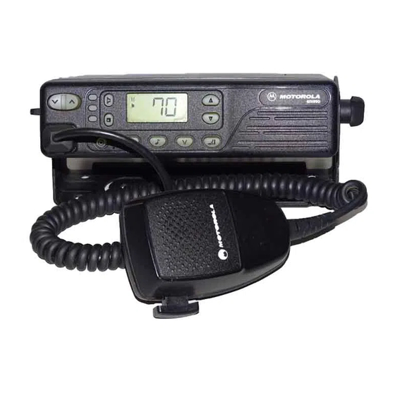
GM950E/GM950i
Mobile Radio
Service Manual
6804111J39-B
Issue: May, 2000
Table of
Contents
Previous
Page
Next
Page
1
2
3
4
5
Advertisement
Chapters
Chapter 2 Model Chart and Accessories
15
Chapter 3 Maintenance
19
Table of Contents
151
Table of Contents
157
Table of Contents
167
Table of Contents
Need help?
Do you have a question about the GM950E and is the answer not in the manual?
Ask a question
Questions and answers
Related Manuals for Motorola GM950E
Radio motorola GM-950 Manual
Control heads/control microphones specific information (18 pages)
Radio Motorola GM-950 Manual
Band specific information (92 pages)
Radio Motorola GM950 Installation Manual
Remote mount kit (10 pages)
Radio Motorola GM950 User Manual
Motorola portable radio user guide (9 pages)
Radio Motorola GM-950 Manual
Control heads/control microphones specific information (16 pages)
Radio Motorola GM-950 Manual
Control heads/control microphones specific information (18 pages)
Radio Motorola GM950i Service Manual
(228 pages)
Radio Motorola GM300 Service Manual
136-162 mhz 146-174 mhz 403-433 mhz 438-470 mhz 465-495 mhz 490-520 mhz (49 pages)
Radio Motorola GM300 Service Manual
146-174 mhz 449-470 mhz (94 pages)
Radio Motorola GM340 User Manual
Professional radio (32 pages)
Radio Motorola GM360 User Manual
Professional radio (60 pages)
Radio Motorola GM360 User Manual
Professional mobile radio (163 pages)
Radio Motorola GM338 Service Manual
Mobile radios (56 pages)
Radio Motorola GM1200 Series User Manual
(19 pages)
Radio Motorola GM350 User Manual
(7 pages)
Radio Motorola GM300 Series Selling Manual
Professional radio (68 pages)
This manual is also suitable for:
Gm950i
Table of Contents
Save PDF
Print
Rename the bookmark
Delete bookmark?
Delete from my manuals?
Login
Sign In
OR
Sign in with Facebook
Sign in with Google
Upload manual
Upload from disk
Upload from URL


Need help?
Do you have a question about the GM950E and is the answer not in the manual?
Questions and answers