Table of Contents
Advertisement
Quick Links
Advertisement
Table of Contents

Related Manuals for Icom IC-M422


Summary of Contents for Icom IC-M422
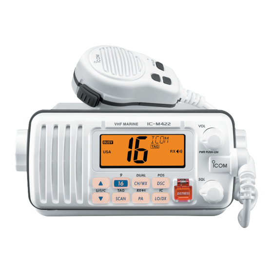
- Page 1 SERVICE MANUAL VHF MARINE TRANSCEIVER iC-m422 S-14131MZ-C1-q Jul. 2006...
- Page 2 8. READ the instructions of test equipment thoroughly before connecting equipment to the transceiver. Icom, Icom Inc. and logo are registered trademarks of Icom Incorporated (Japan) in the United States, the United Kingdom, Germany, France, Spain, Russia and/or other countries.
-
Page 3: Table Of Contents
IC-M422 ........ -
Page 4: Specifications
SECTION 1 SPECIFICATIONS GENERAL • Frequency coverage : TX 156.025–157.425 MHz 156.050–163.275 MHz • Type of emission : 16K0G3E, 16K0G2B (DSC) : 50 Ω (Nominal) • Antenna impedance • Operating temperature range : –4˚F to +140˚F • Power supply requirement : 13.8 V DC ±15% (negative ground) •... - Page 5 • Channel list 1 - 2...
-
Page 6: Inside Views
SECTION 2 INSIDE VIEWS • MAIN UNIT • FRONT UNIT 2 - 1... -
Page 7: Section 3 Disassembly Instructions
SECTION 3 DISASSEMBLY INSTRUCTIONS • • REMOVING THE CASE REMOVING THE MAIN UNIT 1 Unscrew 4 screws, A. 1 Disconnect W2 from the J2 and J3. 2 Disconnect W4 and W5 from the J4 and J5. Note: When replacing the screws, 0.6–0.8 (N.m) 3 Unsolder the antenna connector, C (2 points). -
Page 8: Section 4 Circuit Description
SECTION 4 CIRCUIT DESCRIPTION 4-1 RECEIVER CIRCUITS The converted 1st IF signal from the 1st mixer is passed through the monolithic fi lters (FI1, FI2) to suppress unwant- 4-1-1 ANTENNA SWITCHING CIRCUIT ed signals, and then amplifi ed at the 1st IF amplifi er (Q23). The antenna switching circuit toggles the receive line and the transmit line. -
Page 9: Transmitter Circuits
4-1-6 SQUELCH CIRCUITS 4-2-2 MODULATION CIRCUIT Noise squelch circuit mutes AF output signals when no RF The modulation circuit modulates the VCO oscillating signal signals are received. By detecting noise components in the with the audio signals from the microphone. demodulated AF signals, the squelch circuit switches the AF mute switch ON and OFF. -
Page 10: Pll Circuits
4-3 PLL CIRCUITS 4-4 DSC CIRCUITS 4-3-1 VCO CIRCUIT • DECODING A portion of the demodulated AF signals from the FM IF IC The VCO circuit (Q4, Q5, D3, D4) directly generates both of the (IC2, pin 9) are passed through the LPF (Q38) to fi lter DSC 1st LO frequency for receiving (134.35–141.575 MHz) and the signal. -
Page 11: Power Supply Circuits
4-6 POWER SUPPLY CIRCUITS Port name Description Line Description NMRXD Input port for the NMEA signal. The voltage from the connected DC power supply. Input port for power switch (VR BOARD; R1). Common 5V converted from the HV line at the L5V regulator Low: When [VOL] is pushed. - Page 12 4-7 PORT ALLOCATIONS (continued) Port name Description Input port for the [DSC] key (LOGIC BOARD; S7). Low: [DSC] key is pushed. Input port for the [PA] key (LOGIC BOARD; S6). Low: [PA] key is pushed. Input por t for the [CH/WX] key (LOGIC CH/WX BOARD;...
-
Page 13: Section 5 Adjustment Procedures
SECTION 5 ADJUSTMENT PROCEDURES 5-1 PREPARATION M REQUIRED TEST EQUIPMENTS EQUIPMENT GRADE AND RANGE EQUIPMENT GRADE AND RANGE Output voltage : 13.8 V DC Frequency range : 300–3000 Hz DC power supply Audio generator Current capacity : More than 10 A Measuring range : 1–500 mV Measuring range : 1–30 W... -
Page 14: Frequency Adjustment
5-2 FREQUENCY ADJUSTMENT ADJUSTMENT MEASUREMENT ADJUSTMENT POINT ADJUSTMENT VALUE CONDITION UNIT OPERATION UNIT ADJUST LOCK 1 • Channel : CH16 (156.800 MHz) MAIN Connect a digital multi- 1.1–2.1 V MAIN Verify VOLTAGE • Receiving meter or oscilloscope to the check point "CP1". 2 •... -
Page 15: Transmit Adjustment
5-3 TRANSMIT ADJUSTMENT ADJUSTMENT MEASUREMENT POINT ADJUSTMENT ADJUSTMENT CONDITION VALUE UNIT OPERATION UNIT ADJUST OUTPUT 1 • Channel : CH16 (156.800 MHz) Rear Connect an RF power 23–23.5 W MAIN R112 POWER • Output power : High Panel meter to the antenna •... -
Page 16: Receive Adjustment
5-4 RECEIVE ADJUSTMENT ADJUSTMENT MEASUREMENT POINT ADJUSTMENT ADJUSTMENT CONDITION VALUE UNIT OPERATION UNIT ADJUST SENSITIVITY 1 • Channel : CH16 (156.800 MHz) MAIN Connect a DC volt meter Maximum MAIN L35, L36, L38, • [SQL] : Max. counterclockwise or oscilloscope to the voltage •... -
Page 17: Ic-M422
SECTION 6 PARTS LIST [LOGIC BOARD] 6-1 IC-M422 ORDER [REPLACEMENT UNITS] DESCRIPTION LOCATION ORDER NO. UNIT NAME 7030003430 S.RES ERJ3GEYJ 821 V (820) 87.3/10 7030003520 S.RES ERJ3GEYJ 472 V (4.7 k) 21.4/39.5 0328520101 U M422 #01 FRONT (FRONT+LOGIC+VR+SQL) [BLK] 7030003440 S.RES ERJ3GEYJ 102 V (1 k) 70.9/12... - Page 18 [LOGIC BOARD] [MAIN UNIT] ORDER ORDER DESCRIPTION DESCRIPTION LOCATION LOCATION 5040003230 S.LED RY-SP110UHY24-5M <VKH> 85.7/50.9 6200009560 S.COL MLG1608B R10J-T 66.2/45 5040003230 S.LED RY-SP110UHY24-5M <VKH> 10.5/50.9 6200010840 S.COL MLG1608B 56NJ-T 61.4/42.8 DS10 5040003230 S.LED RY-SP110UHY24-5M <VKH> 85.7/33.5 6200003091 S.COL NLV32T-2R7J 57.3/56.2 DS11 5040003230 S.LED RY-SP110UHY24-5M <VKH>...
- Page 19 [MAIN UNIT] [MAIN UNIT] ORDER ORDER DESCRIPTION DESCRIPTION LOCATION LOCATION R125 7030007990 S.RES ERJ12YJ820U (82) 83.4/69.4 R285 7030003630 S.RES ERJ3GEYJ 393 V (39 k) T 118.9/20.3 R126 7030003670 S.RES ERJ3GEYJ 823 V (82 k) T 105.4/93.6 R286 7030003580 S.RES ERJ3GEYJ 153 V (15 k) T 118.9/21.6 R127 7030003720 S.RES ERJ3GEYJ 224 V (220 k)
- Page 20 [MAIN UNIT] [MAIN UNIT] ORDER ORDER DESCRIPTION DESCRIPTION LOCATION LOCATION 4030006860 S.CER C1608 JB 1H 102K-T 65.4/52.2 C187 4030016930 S.CER ECJ0EB1A104K 79.8/53.2 4030011770 S.CER C1608 CH 1H 060B-T 64.3/50.6 C188 4030017460 S.CER ECJ0EB1E102K 79.7/51.2 4030006850 S.CER C1608 JB 1H 471K-T 65.4/53.5 C189 4030017460 S.CER ECJ0EB1E102K...
-
Page 21: Sql Board
[MAIN UNIT] [VR BOARD] ORDER ORDER DESCRIPTION DESCRIPTION LOCATION LOCATION C345 4030017730 S.CER ECJ0EB1E471K 16/73.9 7210003220 VAR TP96N97A-15.7SK-10KB-2852 C346 4030017460 S.CER ECJ0EB1E102K 50.4/7.5 C347 4030017680 S.CER ECJ0EC1H820J 50.4/6.2 C348 4030017680 S.CER ECJ0EC1H820J 42.2/15.2 8900014010 CBL OPC-1442 C349 4030017460 S.CER ECJ0EB1E102K 42.2/13.9 C351 4030016790 S.CER ECJ0EB1C103K... -
Page 22: Main Unit
SECTION 7 MECHANICAL PARTS AND DISASSEMBLY 7-1 IC-M422 [LOGIC BOARD] [CHASSIS PARTS] REF. NO. ORDER NO. DESCRIPTION QTY. REF. NO. ORDER NO. DESCRIPTION QTY. 6510004880 Connector MR-DSE-01 5030002850 LCD IS08328E 8900014000 Cable OPC-1405 8930066470 LCD contact SRCN-2852-SP-N-W 8900014090 Cable OPC-1489 8930066230 2852 LCD holder 8510016590 Case 2807 CASE [black] 8210020990 2807 reflector... - Page 23 MP40 (C) MP42 (C) MP1 (C) MP13 (C) MP4 (C) NOTE 4 Unit: mm (inch) MP41 (C) Glue MP12 (C) J1 (C) NOTE 4 MP42 (C) MP5 (C) MP14 (C) MP47 (C) NOTE 3 164 (6 28.9 (1 110.4 (4 15 ( MP11 (C) W1 (C)
- Page 24 SECTION 8 SEMICONDUCTOR INFORMATION • TRANSISTOR AND FET’S • DIODES 1SS355 1SV307 DSA3A1 HSM88ASR HVC350BTRF (Symbol: A) (Symbol: TX) (Symbol: Green) (Symbol: C3) (Symbol: B0) Green KDS122 RTK/P KDV214E RTK/P MA2S111 MA77 MA8062-M (Symbol: C3) (Symbol: UO) (Symbol: A) (Symbol: 4B) (Symbol: 6-2) L308CCB (Symbol: T8) 8 - 1...
- Page 25 The combination of this page and the next page shows SECTION 9 BOARD LAYOUTS the unit layout in the same configuration as the actual P.C. Board. 9-1 LOGIC BOARD • TOP VIEW 9-2 VR BOARD • TOP VIEW 9-3 SQL BOARD • TOP VIEW 9 - 1...
- Page 26 The combination of this page and the previous page shows the unit layout in the same configuration as the actual P.C. Board. LOGIC BOARD • BOTTOM VIEW – Internal Speaker VR BOARD • BOTTOM VIEW SQL BOARD • BOTTOM VIEW to HM-150B/SW to REAR CABLE to MAIN Unit J4...
- Page 27 The combination of this page and the next page shows the unit layout in the same configuration as the actual P.C. Board. 9-4 MAIN BOARD • TOP VIEW to ANT CP20 J1 (CHASSIS) MP16 (CHASSIS) C373 C111 C117 C140 C134 C101 C441 C120...
- Page 28 MAIN BOARD The combination of this page and the previous page shows the unit layout in the same configuration as the actual P.C. Board. • BOTTOM VIEW MP16 (CHASSIS) CP19 BLACK to DC POWER CP18 SP– CP17 to REAR CABLE SHIELD to EXT.
- Page 29 SECTION 10 BLOCK DIAGRAM HM-150B/SW FI3: ALFY450E BPFV CERAMIC IC2: TA31136FNG KEYM KEYM FI1: FL-368 D14, D21: FI2: FL-363 Q38: KTC4075 Q23: KTC3880S 21.7 MHz D22: 1SS307 XB15A308 Q22: 3SK131 WXDEC 2ND IF XTAL FRONT UNIT Q21: 3SK131 D25: KDV214E IC15: NJM2211M D26, D27, D28: IC9: LA4425A KDV214E...
- Page 30 SECTION 11 VOLTAGE DIAGRAM 11-1 MAIN UNIT AF/MIC PTTC VCO5 VCO5 KTC4075 BL 0.001 AF/MIC AF/MIC R411 MICG MICG 2.7H 80nH HVC350B-E HVC350B-E PTTC PTTC 2.28V to COMMAND MIC C411 3.99V HM-157B/SW C412 R413 0.01 Optional products R415 0.22 0.001 470p 470p 0.1H W2 OPC-1029 1.5p 470p...
- Page 31 MAIN UNIT 0.001 2.2k R125 C126 Explanatory notes LW-25 L308CCB RA35H1516M-121 0.001 LA-243 LA-243 CP15 C116 C118 C114 C115 C117 0.001 220p VOLTAGE LINE C125 C128 C132 0.001 68nH 0.001 TX LINE MA77 to ANT R126 0.001 LA-253 RX LINE C101 CP20 C127...
- Page 32 11-2 LOGIC BOARD 2SC4081 S TDEC 4.7k EXTTXD 2SA1576 R TC7W14FU F COMTXD COMRXD COMTXD COMRXD /NMEAI 2SK1069-4-TL-E NMEAI 0.001 EXTRXD NMRXD NMEAI 1SS355 PC357NJ0000F EP81 / NMEAI 0.001 0.068 KRC414 0.01 NMEAI+ 1SS355 NMEAI– to REAR CABLE ICF3 0.01 4.7k NMEAO CH/WX P14/KI4 P63/TXD0...
-
Page 33: Voltage Diagram
12-2 VOLTAGE DIAGRAM SECTION 12 HM-150B/SW KUC3523-040245 12-1 MECHANICAL PARTS AND DISASSEMBLY [CHASSIS PARTS] [MAIN PARTS] 0.022 CHASSIS UNIT REF. NO. ORDER NO. DESCRIPTION QTY. REF. NO. ORDER NO. DESCRIPTION QTY. W1 OPC1081 [BLK] OPC1082 [SW] 8900012212 Cable OPC-1249B [HM-150B] 7700002640 MIC KUC3523-040245 8900013570... - Page 34 Phone : +34 (93) 590 26 70 Fax : +34 (93) 589 04 46 Glenwood Centre #150-6165 : http://www.icomspain.com Highway 17 Delta, B.C., V4K 5B8, Canada E-mail : icom@icomspain.com Phone : +1 (604) 952-4266 Fax : +1 (604) 952-0090 : http://www.icomcanada.com E-mail : info@icomcanada.com Unit 9, Sea St., Herne Bay, Kent, CT6 8LD, U.K.
- Page 35 S-14131MZ-C1-q © 2005–2006 Icom Inc.
Need help?
Do you have a question about the IC-M422 and is the answer not in the manual?
Questions and answers