Table of Contents
Advertisement
Advertisement
Table of Contents

Related Manuals for Icom IC-M422


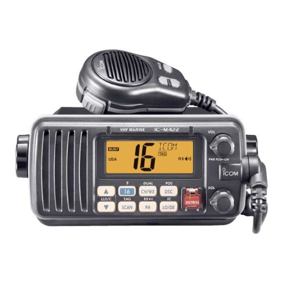
Summary of Contents for Icom IC-M422
- Page 1 iC-m422...
- Page 2 8. READ the instructions of test equipment thoroughly before connecting equipment to the transceiver. Icom, Icom Inc. and logo are registered trademarks of Icom Incorporated (Japan) in the United States, the United Kingdom, Germany, France, Spain, Russia and/or other countries.
-
Page 3: Table Of Contents
IC-M422 ........ -
Page 4: Specifications
SECTION 1 SPECIFICATIONS GENERAL • Frequency coverage : TX 156.025–157.425 MHz 156.050–163.275 MHz • Type of emission : 16K0G3E, 16K0G2B (DSC) : 50 Ω (Nominal) • Antenna impedance • Operating temperature range : –4˚F to +140˚F • Power supply requirement : 13.8 V DC ±15% (negative ground) •... - Page 5 • CHANNEL LISTS . y l , s l y l l c i l 1 - 2...
-
Page 6: Inside Views
SECTION 2 INSIDE VIEWS • MAIN UNIT • FRONT UNIT 2 - 1... -
Page 7: Section 3 Disassembly Instructions
SECTION 3 DISASSEMBLY INSTRUCTIONS • • REMOVING THE CASE REMOVING THE MAIN UNIT 1 Unscrew 4 screws, A. 1 Disconnect W2 from the J2 and J3. 2 Disconnect W4 and W5 from the J4 and J5. Note: When replacing the screws, 0.6–0.8 (N.m) 3 Unsolder the antenna connector, C (2 points). -
Page 8: Section 4 Circuit Description
SECTION 4 CIRCUIT DESCRIPTION 4-1 RECEIVER CIRCUITS The converted 1st IF signal from the 1st mixer is passed through the monolithic fi lters (FI1, FI2) to suppress unwant- 4-1-1 ANTENNA SWITCHING CIRCUIT ed signals, and then amplifi ed at the 1st IF amplifi er (Q23). The antenna switching circuit toggles the receive line and the transmit line. -
Page 9: Transmitter Circuits
4-1-6 SQUELCH CIRCUITS 4-2-2 MODULATION CIRCUIT Noise squelch circuit mutes AF output signals when no RF The modulation circuit modulates the VCO oscillating signal signals are received. By detecting noise components in the with the audio signals from the microphone. demodulated AF signals, the squelch circuit switches the AF mute switch ON and OFF. -
Page 10: Pll Circuits
4-3 PLL CIRCUITS 4-4 DSC CIRCUITS 4-3-1 VCO CIRCUIT • DECODING A portion of the demodulated AF signals from the FM IF IC The VCO circuit (Q4, Q5, D3, D4) directly generates both of the (IC2, pin 9) are passed through the LPF (Q38) to fi lter DSC 1st LO frequency for receiving (134.35–141.575 MHz) and the signal. -
Page 11: Power Supply Circuits
4-6 POWER SUPPLY CIRCUITS Port name Description Line Description NMRXD Input port for the NMEA signal. The voltage from the connected DC power supply. Input port for power switch (VR BOARD; R1). Common 5V converted from the HV line at the L5V regulator Low: When [VOL] is pushed. - Page 12 4-7 PORT ALLOCATIONS (continued) Port name Description Input port for the [DSC] key (LOGIC BOARD; S7). Low: [DSC] key is pushed. Input port for the [PA] key (LOGIC BOARD; S6). Low: [PA] key is pushed. Input por t for the [CH/WX] key (LOGIC CH/WX BOARD;...
-
Page 13: Section 5 Adjustment Procedures
SECTION 5 ADJUSTMENT PROCEDURES 5-1 PREPARATION M REQUIRED TEST EQUIPMENTS EQUIPMENT GRADE AND RANGE EQUIPMENT GRADE AND RANGE Output voltage : 13.8 V DC Frequency range : 300–3000 Hz DC power supply Audio generator Current capacity : More than 10 A Measuring range : 1–500 mV Measuring range : 1–30 W... -
Page 14: Frequency Adjustment
5-2 FREQUENCY ADJUSTMENT ADJUSTMENT MEASUREMENT ADJUSTMENT POINT ADJUSTMENT VALUE CONDITION UNIT OPERATION UNIT ADJUST LOCK 1 • Channel : CH16 (156.800 MHz) MAIN Connect a digital multi- 1.1–2.1 V MAIN Verify VOLTAGE • Receiving meter or oscilloscope to the check point "CP1". 2 •... -
Page 15: Transmit Adjustment
5-3 TRANSMIT ADJUSTMENT ADJUSTMENT MEASUREMENT POINT ADJUSTMENT ADJUSTMENT CONDITION VALUE UNIT OPERATION UNIT ADJUST OUTPUT 1 • Channel : CH16 (156.800 MHz) Rear Connect an RF power 23–23.5 W MAIN R112 POWER • Output power : High Panel meter to the antenna •... -
Page 16: Receive Adjustment
5-4 RECEIVE ADJUSTMENT ADJUSTMENT MEASUREMENT POINT ADJUSTMENT ADJUSTMENT CONDITION VALUE UNIT OPERATION UNIT ADJUST SENSITIVITY 1 • Channel : CH16 (156.800 MHz) MAIN Connect a DC volt meter Maximum MAIN L35, L36, L38, • [SQL] : Max. counterclockwise or oscilloscope to the voltage •... -
Page 17: Ic-M422
SECTION 6 PARTS LIST 6-1 IC-M422 [LOGIC BOARD] ORDER DESCRIPTION [REPLACEMENT UNITS] LOCATION 7030008121 S.RES ERA3YED 682V 34.5/7.7 ORDER NO. UNIT NAME 7030003860 S.RES ERJ3GE JPW V 33.2/10.5 7030003250 S.RES ERJ3GEYJ 270 V (27 Ω) 0328520101 U M422 #01 FRONT (FRONT+LOGIC+VR+SQL) 71.9/22.7... - Page 18 [LOGIC BOARD] [MAIN UNIT] ORDER ORDER DESCRIPTION DESCRIPTION LOCATION LOCATION 6510018970 S.CNR B4B-PH-SM3-TB 76.2/6.5 1750001190 S.VCP KDV214E RTK/P 86.9/61.2 6510022310 S.CNR B5B-PH-SM3-TB 22.3/8 1790000700 DIO DSA3A1 6510021720 S.CNR 30FLT-SM1-TB 55.4/11.8 6510021720 S.CNR 30FLT-SM1-TB 38.5/17.8 6510019420 S.CNR B8B-ZR-SM3-TF 84.5/24.6 2030000350 MLH 21R15AB (FL-368) 2030000270 MLH FL-363 (21.7 MHz)
- Page 19 [MAIN UNIT] [MAIN UNIT] ORDER ORDER DESCRIPTION DESCRIPTION LOCATION LOCATION R267 7030003800 S.RES ERJ3GEYJ 105 V (1 MΩ) 30.2/22.1 R106 7510001651 S.THM NTCG16 4BH 222JT 72.3/75 R107 7030003500 S.RES ERJ3GEYJ 332 V (3.3 kΩ) 72.3/76.3 R268 7030003800 S.RES ERJ3GEYJ 105 V (1 MΩ) 31.6/20 R108 7030003860 S.RES ERJ3GE JPW V...
- Page 20 [MAIN UNIT] [MAIN UNIT] ORDER ORDER DESCRIPTION DESCRIPTION LOCATION LOCATION C173 4030011770 S.CER C1608 CH 1H 060B-T 93.9/57.5 4030009920 S.CER C1608 CH 1H 050B-T 62.3/49.6 4030007050 S.CER C1608 CH 1H 220J-T 64.2/42.8 C174 4030009910 S.CER C1608 CH 1H 040B-T 96/56.8 4030007060 S.CER C1608 CH 1H 270J-T 62.4/45 C175...
-
Page 21: Hm-150B/Sw
[MAIN UNIT] [VR BOARD] ORDER ORDER DESCRIPTION DESCRIPTION LOCATION LOCATION C331 4030006900 S.CER C1608 JB 1H 103K-T 51.5/4.4 7210003220 VAR TP96N97A-15.7SK-10KB-2852 C332 4030006860 S.CER C1608 JB 1H 102K-T 42.1/7.1 C333 4030006900 S.CER C1608 JB 1H 103K-T 42.1/5.8 C334 4030007050 S.CER C1608 CH 1H 220J-T 63.7/21.7 8900014010 CBL OPC-1442... -
Page 22: Section Mechanical Parts And Disassembly
SECTION 7 MECHANICAL PARTS AND DISASSEMBLY 7-1 IC-M422 [LOGIC BOARD] [CHASSIS PARTS] REF. NO. ORDER NO. DESCRIPTION QTY. REF. NO. ORDER NO. DESCRIPTION QTY. 6510004880 Connector MR-DSE-01 5030002850 LCD IS08328E 8900014000 Cable OPC-1405 <TJM> 8930066470 LCD contact SRCN-2852-SP-N-W 8900014090 Cable OPC-1489 <AI>... - Page 23 7 - 2...
- Page 24 SECTION 8 SEMICONDUCTOR INFORMATION • TRANSISTOR AND FET’S • DIODES 8 - 1...
- Page 25 The combination of this page and the next page shows SECTION 9 BOARD LAYOUTS the unit layout in the same configuration as the actual P.C. Board. 9 - 1...
- Page 26 The combination of this page and the previous page shows the unit layout in the same configuration as the actual P.C. Board. 9 - 2...
- Page 27 The combination of this page and the next page shows the unit layout in the same configuration as the actual P.C. 9 - 3...
- Page 28 The combination of this page and the previous page shows the unit layout in the same configuration as the actual P.C. Board. 9 - 4...
- Page 29 SECTION 10 BLOCK DIAGRAM 10 - 1...
-
Page 30: Main Unit
SECTION 11 VOLTAGE DIAGRAM 11-1 MAIN UNIT 11 - 1... - Page 31 11 - 2...
- Page 32 11-2 LOGIC BOARD 11 - 3...
- Page 33 12-2 VOLTAGE DIAGRAM SECTION 12 HM-150B/SW KUC3523-040245 12-1 MECHANICAL PARTS AND DISASSEMBLY [CHASSIS PARTS] [MAIN PARTS] 0.022 CHASSIS UNIT REF. NO. ORDER NO. DESCRIPTION QTY. REF. NO. ORDER NO. DESCRIPTION QTY. W1 OPC1081 [BLK] OPC1082 [SW] 8900012212 Cable OPC-1249B [HM-150B] 7700002640 MIC KUC3523-040245 8900013570...
- Page 34 : http://www.icomspain.com Highway 17 Delta, B.C., V4K 5B8, Canada Phone : +1 (604) 952-4266 Fax : +1 (604) 952-0090 E-mail : icom@icomspain.com : http://www.icomcanada.com E-mail : info@icomcanada.com Unit 9, Sea St., Herne Bay, Kent, CT6 8LD, U.K. Phone : +44 (01227) 741741 Fax : +44 (01227) 741742 : http://www.icomuk.co.uk...
- Page 35 S-14131MZ-C1 © 2005 Icom Inc.
Need help?
Do you have a question about the IC-M422 and is the answer not in the manual?
Questions and answers