Table of Contents
Advertisement
Advertisement
Table of Contents

Subscribe to Our Youtube Channel
Related Manuals for Icom IC-M401E


Summary of Contents for Icom IC-M401E
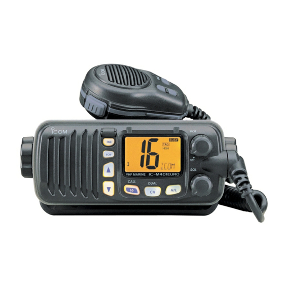
- Page 1 SERVICE MANUAL VHF MARINE TRANSCEIVER iC-m401e...
- Page 2 8. READ the instructions of test equipment thoroughly before connecting equipment to the transceiver. Icom, Icom Inc. and are registered trademarks of Icom Incorporated (Japan) in the United States, the United Kingdom, Germany, France, Spain, Russia and/or other countries.
-
Page 3: Table Of Contents
IC-M401E ........ -
Page 4: Specifications
SECTION 1 SPECIFICATIONS ‘ ‘ GENERAL • Frequency coverage : 156.000–161.450 MHz (Tx) 156.000–163.425 MHz (Rx) • Mode : 16K0G3E (FM) 16K0G2B (DSC) • Power supply requirement : 13.8 V DC (negative ground) • Usable temperature range : –20˚C to +60˚C •... -
Page 5: Vhf Marine Channel List
‘ ‘ VHF MARINE CHANNEL LIST Channel No. Frequency (MHz) Channel No. Frequency (MHz) Channel No. Frequency (MHz) USA * USA * USA * Transmit Receive Transmit Receive Transmit Receive 156.050 160.650 157.100 161.700 156.725 156.725 156.050 156.050 157.100 157.100 156.775 156.775 156.100... -
Page 6: Inside Views
SECTION 2 INSIDE VIEWS • MAIN-E UNIT Pre-driver YGR amplifier (Q10: 2SC4226) (Q12: 2SC3775) Power amplifier (IC3: RA35H1516M-01) PLL reference oscillator (X1: CR-768) PLL IC (IC1: µPD3140GS) Antenna switching circuit (D14, D21: XB15A308) RF amplifier (Q21: 3SK131) VCO circuit 1st mixer (Q22: 3SK131) AF mute 2nd IF filter... -
Page 7: Section 3 Disassembly Instructions
SECTION 3 DISASSEMBLY INSTRUCTIONS • • REMOVING THE CASE REMOVING THE MAIN-E UNIT 1 Unscrew 6 screws, A. 1 Remove the shield covers, MP31 and MP33. 2 Unsolder the antenna connector, B (1 point). Note: When replacing the screw, 10–12 kg of torque MUST 3 Unsolder bottom side [A] (6 points), and side [B] (1 point), be applied to ensure water resistance. -
Page 8: Section 4 Circuit Description
SECTION 4 CIRCUIT DESCRIPTION 4-1 RECEIVER CIRCUITS The signals from the RF circuit are mixed with the VCO sig- nals at the 1st mixer circuit (Q22) to produce a 21.7 MHz 1st 4-1-1 ANTENNA SWITCHING CIRCUIT IF signal. (MAIN-E UNIT) The antenna switching circuit functions as a low-pass filter The 1st IF signal is applied to two crystal filters (FI1, FI2) to while receiving and as resonator circuit while transmitting. -
Page 9: Transmitter Circuits
4-1-5 AF AMPLIFIER CIRCUIT 4-2 TRANSMITTER CIRCUITS (MAIN-E AND FRONT UNITS) 4-2-1 MICROPHONE AMPLIFIER CIRCUIT The AF amplifier circuit amplifies the detected signals to (MAIN-E UNIT) drive a speaker. The AF circuit includes an AF mute circuit The microphone amplifier circuit amplifies audio signals with for the squelch. -
Page 10: Pll Circuits
4-2-4 POWER AMPLIFIER CIRCUIT (MAIN-E UNIT) 4-3 PLL CIRCUITS The power amplifier circuit amplifies the driver signal to an 4-3-1 GENERAL output power level. The PLL circuit provides stable oscillation of the transmit fre- quency and receive 1st LO frequency. The PLL circuit com- IC3 is a power module which has amplification output capa- pares the phase of the divided VCO frequency to the refer- bilities of about 35 W with 50 mW input. -
Page 11: Dsc Circuits
4-3-2 TX AND RX LOOP (MAIN-E UNIT) • RESET CIRCUIT IC2 is a reset IC. When turn power ON, IC2 outputs a reset The generated signal at the VCO (Q4, Q5, D3, D4) enters signal (“LOW” pulse) to the CPU (IC1, pin 15) via the “RES” the PLL IC (IC1, pin 2) and is divided at the programmable line. -
Page 12: Port Allocations
4-7 PORT ALLOCATIONS 4-7-1 CPU (LOGIC-E BOARD; IC1) Port Port Description Description number name number name Outputs control signal for the LCD Input port for the HM-132 functions. contrast. 2.02 V: [Y] is pushed. KEYM CONT1 3.00 V: [Z] is pushed. CONT2 CONT1 CONTRAST... -
Page 13: Section 5 Adjustment Procedures
SECTION 5 ADJUSTMENT PROCEDURES 5-1 PREPARATION I REQUIRED TEST EQUIPMENT EQUIPMENT GRADE AND RANGE EQUIPMENT GRADE AND RANGE Output voltage : 13.8 V DC Frequency range : 300–3000 Hz DC power supply Audio generator Current capacity : 10 A or more Measuring range : 1–500 mV Measuring range... -
Page 14: Pll Adjustments
5-2 PLL ADJUSTMENTS ADJUSTMENT MEASUREMENT POINT ADJUSTMENT ADJUSTMENT CONDITION VALUE UNIT LOCATION UNIT ADJUST LOCK • Operating channel : ch16 MAIN-E Connect a digital 1.8 V Verify VOLTAGE • Receiving multi-meter or oscil- loscope check point CP1. • Operating channel : ch16 1.6 V •... -
Page 15: Transmitter Adjustments
5-3 TRANSMITTER ADJUSTMENTS ADJUSTMENT MEASUREMENT POINT ADJUSTMENT ADJUSTMENT CONDITION VALUE UNIT LOCATION UNIT ADJUST OUTPUT • Operating channel : ch16 Rear Connect 23 W MAIN R114 POWER • Output power : High Panel power meter to the • Transmitting antenna connector. FREQUENCY •... - Page 16 R114 Output power adjustment Sensitivity adjustment R327 Frequency deviation adjustment Squelch level check point R214 Squelch level adjustment Sensitivity check point – [PTT] Audio generator – AC millivoltmeter 5 - 4...
-
Page 17: Section 6 Parts List
SECTION 6 PARTS LIST 6-1 IC-M401E [MAIN-E UNIT] [MAIN-E UNIT] ORDER ORDER DESCRIPTION DESCRIPTION 1130007610 S.IC µPD3140GS-E1 (DS8) 6200002430 S.COIL NL 252018T-082J 1110003200 S.IC TA31136FN (EL) 6200009620 S.COIL MLG1608B 68NJ-T 1150002080 RA35H1516M-01 6200002600 S.COIL NL 252018T-047J 1130007300 S.IC TC4W66FU (TE12L) 6200002600 S.COIL... - Page 18 [MAIN-E UNIT] [MAIN-E UNIT] ORDER ORDER DESCRIPTION DESCRIPTION R126 7030005420 S.RESISTOR ERJ3GEYJ 202 V (2 kΩ) R324 7510001670 S.THRMISTOR NTCG16 4BH 103KT R127 7030005420 S.RESISTOR ERJ3GEYJ 202 V (2 kΩ) R325 7030003570 S.RESISTOR ERJ3GEYJ 123 V (12 kΩ) ERJ3GEYJ 150 V (15 Ω) R141 7030003220 S.RESISTOR...
- Page 19 [MAIN-E UNIT] [MAIN-E UNIT] ORDER ORDER DESCRIPTION DESCRIPTION C101 4030007050 S.CERAMIC C1608 CH 1H 220J-T C231 4030011810 S.CERAMIC C1608 JB 1A 224K-T C102 4030007040 S.CERAMIC C1608 CH 1H 180J-T C232 4030011600 S.CERAMIC C1608 JB 1E 104K-T C103 4030007080 S.CERAMIC C1608 CH 1H 390J-T C233 4030008880 S.CERAMIC...
- Page 20 [MAIN-E UNIT] [LOGIC-E BOARD] ORDER ORDER DESCRIPTION DESCRIPTION C415 4030008470 S.CERAMIC C1608 JB 1H 272K-T 1140011930 S.IC HD6433847RB82H (FX-2706B) C416 4030006860 S.CERAMIC C1608 JB 1H 102K-T 1110005770 S.IC S-80942CNMC-G9C-T2 1130007570 S.IC BU4094BCFV-E2 1130009680 S.IC HN58X2432TI 6330001670 RELAY FTR-P3CP012W1 1130005290 S.IC TC74HC14AF 1170000350 S.IC...
- Page 21 [LOGIC-E BOARD] [VR BOARD] ORDER ORDER DESCRIPTION DESCRIPTION 7030003560 S.RESISTOR ERJ3GEYJ 103 V (10 kΩ) 7210002350 VARIABLE TP96N97N15F-10KA-1301 7030003490 S.RESISTOR ERJ3GEYJ 272 V (2.7 kΩ) 7030003800 S.RESISTOR ERJ3GEYJ 105 V (1 MΩ) 7030003680 S.RESISTOR ERJ3GEYJ 104 V (100 kΩ) 8900010820 CABLE OPC-1099 <CMI>...
- Page 22 6-2 HM-132 [MAIN UNIT] ORDER DESCRIPTION 7010007640 RESISTOR FRD25 T2-123J (12 kΩ) 7010007630 RESISTOR FRD25 T2-682J (6.8 kΩ) 7010007650 RESISTOR FRD25 T2-153J (15 kΩ) 7010007660 RESISTOR FRD25 T2-333J (33 kΩ) 4030018550 S.CERAMIC C1608 JB 1H 223K-T 4030011340 S.CERAMIC C1608 CH 1H 471J-T 7700002500 MICROPHONE KUC3523-040245...
-
Page 23: Ic-M401E
SECTION 7 MECHANICAL PARTS AND DISASSEMBLY 7-1 IC-M401E [CHASSIS PARTS] [LOGIC-E BOARD] REF. NO. ORDER NO. DESCRIPTION QTY. REF. NO. ORDER NO. QTY. DESCRIPTION 6510004880 Connector MR-DS-E 01 DS 1 5030001950 LCD TTR5341 8900010710 Cable OPC-1087 (nut, w/gasket) <LIA> EP 2... - Page 24 Unit: mm MP26 (C) MP25 (C) MP33 (C) MP13 (C) MP20 (C) 32.1 86.5 MP42 (C) MP12 (C) MP42 (C) J1 (C) MP5 (C) MP43 (C) MP42 (C) MP4 (C) MP43 (C) MP14 (C) W2 (C) MP40 (C) MP42 (C) MP42 (C) MP43 (C) MP45 (C)
-
Page 25: Hm-132
8610010870 2352 hanger knob MP10 8310048760 2352 R-plate MP11 8310048780 2352 MIC plate MP12 8820001150 2352 screw MP13 8850001850 ICOM washer (Y) MP14 8930052340 O-ring (AE) MP15 8930052350 O-ring (AF) MP16 8930056460 2449 MIC sheet MP17 8930054910 2449 SP Rubber... -
Page 26: Section 8 Semi-Conductor Information
SECTION 8 SEMI-CONDUCTOR INFORMATION • TRANSISTOR AND FET’S 2SB1132 R 2SC2714 Y 2SA1576A R 2SA1577 Q 2SA1588 GR (Symbol: BAR) (Symbol: QY) (Symbol: FR) (Symbol: HQ) (Symbol: ZG) 2SC4215 O 2SC3775 3 2SC4081 R 2SC4116 BL 2SC4226 R25 (Symbol: QO) (Symbol: OY3) (Symbol: BR) (Symbol: LL) -
Page 27: Section 9 Board Layouts
SECTION 9 BOARD LAYOUTS 9-3 HM-132 • TOP VIEW 9-1 VR BOARD • TOP VIEW to MAIN-E unit J5 OPC-1099 to SQL board • BOTTOM VIEW • BOTTOM VIEW 9-2 SQL BOARD • TOP VIEW • BOTTOM VIEW 9 - 1... - Page 28 The combination of this page and the next page shows the unit layout in the same configuration as the actual 9-4 LOGIC-E BOARD P.C. Board. • TOP VIEW SP– – to Smart MIC to DS-100 (OPC-1087) (HM-132) to MAIN-E unit J6 (W3: OPC-1046) 9 - 2...
- Page 29 The combination of this page and the previous page shows the unit layout in the same configuration as the • BOTTOM VIEW actual P.C. Board. 9 - 3...
- Page 30 to DS-100 DATAS– The combination of this page and the next page shows the DATAM+ ICF3 unit layout in the same configuration as the actual P.C. Board. DATAM– 9-5 MAIN-E UNIT DATAS+ DATAS+ DATAS– LOGIC-E • TOP VIEW ICF3 board J1 DSC–...
- Page 31 • BOTTOM VIEW to EXT SPEAKER to DC POWER SP– CP19 CP18 CP17 CP16 The combination of this page and the previous page shows the unit layout in the same configuration as the actual P.C. Board. 9 - 5...
-
Page 32: Vr Board
SECTION 10 BLOCK DIAGRAM MAIN-E UNIT EXT SP FRONT UNIT HM-132 IC9: LA4425A INT SP FI3: CFWS450F CERAMIC IC2: TA31136FN RMUTM VR BOARD D14, D21: FI1: FL-368 IC4A: XB15A308 × 2 Q31: 2SC4116 FI2: FL-363 TC4W66FU Q22: 3SK131 2ND IF XTAL MUTE D26, D27, D28:... -
Page 33: Voltage Diagram
SECTION 11 VOLTAGE DIAGRAM 11-1 LOGIC-E BOARD PC357N6T MA8062-M LOGIC-E BOARD 0.0047 1SS355 0.01 6.8k Explanatory notes 5.01V BAND EXTENTION VOLTAGE LINE DATAM+ 13.37V MA8062-M DATAM– TX LINE to DSC terminal DATAS+ 2SC4081 0.01 RX LINE DATAS– DS-100 ICF3 (OPC-1087) 0.001 MA8062-M MA8062-M... -
Page 34: Main-E Unit
11-2 MAIN-E UNIT VCO5 RA35H1516M 0.001 0.001 2SC4116 R123 C126 2.2k to ANT 2.7µH 80nH LW-25 3.97V XB15A308 0.001 LA-243 LA-243 HVC350BTRF CP15 C146 C107 C108 C109 C110 68nH 2.2k 0.001 470p 0.001 C101 C125 2.45V 470p 0.22 0.001 0.1µH 56nH MA77 1.5p... -
Page 35: Hm-132
11-3 HM-132 KUC3523-040245 0.022 CHASSIS UNIT W1 OPC-1081 (Black) OPC-1082 (White) SKHHLP014A MICG to MAIN-E unit J4 2.0V Z ON 3.0V 16/C ON 3.8V SKHHAM024A 6.8k KEYM UP [Y] to LOGIC-E board J3 SKHHAM024A DOWN [Z] SKHHAM024A 16/C 11 - 3... - Page 37 S-14013MZ-C2 1-1-32, Kamiminami, Hirano-ku, Osaka 547-0003, Japan © 2004 Icom Inc.
Need help?
Do you have a question about the IC-M401E and is the answer not in the manual?
Questions and answers