Sony CCD-TRV32 Service Manual
Video camera recorder
Hide thumbs
Also See for CCD-TRV32:
- Service manual (33 pages) ,
- Operating instructions manual (76 pages) ,
- Operating instructions manual (76 pages)
Table of Contents
Advertisement
Quick Links
CCD-TRV32/TRV34/TRV34PK/TRV44/TRV52/TRV53/TRV312/TRV512 ( NTSC )
SERVICE MANUAL
B MECHANISM
• CCD-TRV34PK is model that carring bag are added
in CCD-TRV34.
• CCD-TRV34PK is different from CCD-TRV34 only
in the accessory and packing materials.
MICROFILM
CCD-TRV14E/TRV24E/TRV44E ( PAL )
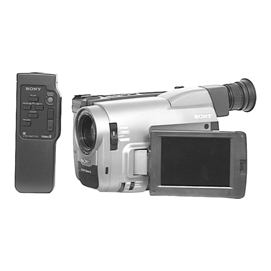
Photo : CCD-TRV53
SPECIFICATIONS
CCD-TRV32/TRV52/TRV53/
TRV312/TRV512(NTSC)
Canadian Model
CCD-TRV14E/TRV24E(PAL)
CCD-TRV34/TRV34PK/TRV44(NTSC)
CCD-TRV14E/TRV24E/TRV44E(PAL)
Australian Model
CCD-TRV14E/TRV24E/TRV44E(PAL)
Hong Kong Model
CCD-TRV34/TRV44(NTSC)
CCD-TRV14E/TRV24E/TRV44E(PAL)
Tourist Model
CCD-TRV14E/TRV24E/TRV44E(PAL)
For MECHANISM ADJUSTMENT, refer to
the "8mm Video MECHANICAL
ADJUSTMENT MANUAL
— Continued on next page —
VIDEO CAMERA RECORDER
RMT-713
US Model
CCD-TRV53(NTSC)
AEP Model
UK Model
E Model
CCD-TRV34(NTSC)
" (9-973-801-11).
Advertisement
Table of Contents


Need help?
Do you have a question about the CCD-TRV32 and is the answer not in the manual?
Questions and answers