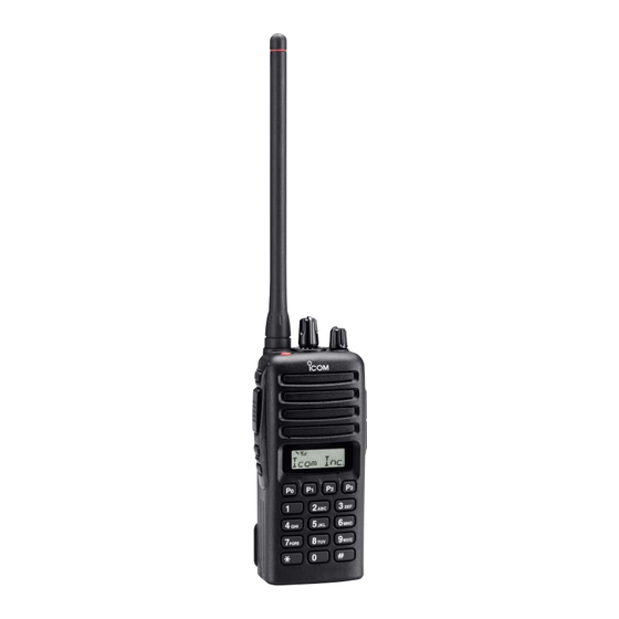
Icom IC-F33GT Service Manual
Vhf
Hide thumbs
Also See for IC-F33GT:
- Instruction manual (56 pages) ,
- Service manual (37 pages) ,
- Instruction manual (48 pages)

Subscribe to Our Youtube Channel
Related Manuals for Icom IC-F33GT


Summary of Contents for Icom IC-F33GT
- Page 1 VHF TRANSCEIVER iC-f33gt iC-f33gs iC-f34gt iC-f34gs S-14113IZ-C1-q Apr. 2007...
- Page 2 8. READ the instructions of test equipment throughly before connecting a test equipment to the transceiver. Icom, Icom Inc. and logo are registered trademarks of Icom Incorporated (Japan) in the United States, the United Kingdom, Germany, France, Spain, Russia and/or other countries.
-
Page 3: Table Of Contents
CONTENTS SECTION SPECIFICATIONS SECTION INSIDE VIEWS SECTION DISASSEMBLY INSTRUCTIONS SECTION OPTIONAL UNITS INSTALLATION SECTION CIRCUIT DESCRIPITON RECEIVER CIRCUITS............5-1 TRANSMITTER CIRCUITS . -
Page 4: Specifications
SECTION 1 SPECIFICATIONS ■ GENERAL • Frequency coverage : 136.000–174.000 MHz • Mode : FM • Type of emission VERSION WIDE MIDDLE NARROW [USA], [GEN] 11K0F3E (12.5 kHz) 16K0F3E (25.0 kHz) [EUR] 14K0F3E (20.0 kHz) 8K50F3E (12.5 kHz) • Number of conventional channels : 256 ch, 16 banks : 50 Ω... -
Page 5: Inside Views
SECTION 2 INSIDE VIEWS • MAIN UNIT TOP VIEW BOTTOM VIEW AF amplifier (IC15: TA7368F) +5 Regulator APC amplifier IF amplifier (IC17: NJM2870) (IC2: TA75S01F) (Q7: 2SC4215) TX Mute switch TX/RX switch FM IF IC (Q501: UNR9213J) (D16, D17: MA2S077) (IC9: TA31136FN) VCO circuits PLL IC... - Page 6 SECTION 3 DISASSEMBLY INSTRUCTION • REMOVING THE CHASSIS UNIT • REMOVING THE PA UNIT 1 Unscrew 1 nut A, and remove 2 knobs B, C. 1 Unscrew 3 screws M. 2 Unscrew 2 screws D. 2 Unsolder 4 points N, and take off the PA unit in the 3 Unscrew 2 screws E.
-
Page 7: Optional Units Installation
SECTION 4 OPTIONAL UNIT INSTALLATION l l a o l l l l a fl fl u l l o l l , s i t f i l s ’ t ™ ™ next page. n i l , t f a l i above. - Page 8 n i l above. - r i a l l o i t l l a l l a above. ™ 4 - 2...
-
Page 9: Receiver Circuits
SECTION 5 CIRCUIT DESCRIPTION 1ST IF CIRCUITS 5-1 RECEIVER CIRCUITS The 1st IF circuits consist of 1st mixer, 1st IF fi lter and 1st IF RF CIRCUITS amplifi er, and converts the received signals into the 1st IF RF circuits consist of RF fi lters, antenna switch, preamplifi er, signal, fi... -
Page 10: Transmitter Circuits
The filtered signals pass through the high-pass filter to sup- • TONE SQUELCH The tone squelch connects the RX AF line to emit the AF press unwanted harmonic components. The signals pass output signals only when receiving a signal which consists through (or bypass) scrambler and expander sections. - Page 11 MODULATION CIRCUIT APC CIRCUIT • VOICE SIGNAL The APC (Automatic Power Control) circuit stabilizes transmit output power to prevent transmit output power level The modulation circuit FM-modulates the VCO oscillating change which is caused by load mismatching or heat effect, signal with the AF signals from the TX AF circuit.
-
Page 12: Frequency Synthesizer Circuits
A portion of VCO output is applied to the PLL IC via buffer 5-3 FREQUENCY SYNTHESIZER CIRCUITS and harmonic filter. The applied VCO output is divided according to the serial data including divid ratio from A VCO is an oscillator which its oscillation frequency is the CPU, at the prescaler and programmable divider. -
Page 13: Port Allocations
5-6 PORT ALLOCATIONS Port Description Number name 5-6-1 D/A CONVERTOR IC (IC12) Input port for CTCSS/DTCS signal Port CDEC Description from the amplifi er (IC19, pin 1). Number name Input port for the detect signal for Outputs the modulation balance level BATV connecting battery pack’s voltage. -
Page 14: Preparation
SECTION 6 ADJUSTMENT PROCEDURE 6-1 PREPARATION When adjusting IC-F33GT/GS/F34GT/GS, optional CS-F33G ADJ (Rev. 1.0 or later), OPC-478 ADJUSTMENT SOFTWARE CLONING (RS-232C type), OPC-478U/UC (USB type) and a JIG CABLE (see illustration at page 6-2) are required. CABLE CLONING CABLE ▄ REQUIRED TEST EQUIPMENT... - Page 15 AC millivoltmeter To [MIC] Audio generator to the antenna connector Standard signal generator Personal 0.1 µV to 32 mV computer (Ð127 dBm to Ð17 dBm) CAUTION! DO NOT transmit while an SSG is connected to the antenna connector. OPC-478 to RS-232C port Attenuator deviation meter 20 dB or 30 dB...
- Page 16 • CS-F33G ADJ'S SCREEN EXAMPLE NOTE: The above values for settings are example only. Each transceiver has its own specific values for each setting. q: Transceiver's connection state !1 : CTCSS/DTCS deviation w: Reload adjustment data !2 : Squelch level e: Receive sensitivity measurement !3 : Reference frequency r: Connected DC voltage measurement...
- Page 17 6-2 SOFTWARE ADJUSTMENT (TRANSMITTING) Select an operation using [↑] / [↓]keys, then set specifi ed value using [←] / [→] keys on the connected computer keyboard MEASUREMENT ADJUSTMENT ADJUSTMENT CONDITION VALUE UNIT LOCATION PLL LOCK 1 • Operating Channel : CH7 Check the "LVIN"...
-
Page 18: Software Adjustments
SOFTWARE ADJUSTMENT (RECEIVING) • Select an operation using [↑] / [↓]keys, then set specifi ed value using [←] / [→] keys on the connected computer keyboard • Need to adjust "S-METER ADJUSTMENT" after "RX SENSITIVITY ADJUSTMENT" is adjusted. Otherwise , "S-METER ADJUSTMENT" will not be adjusted properly. MEASUREMENT ADJUSTMENT ADJUSTMENT CONDITION... -
Page 19: Main Unit
SECTION 7 PARTS LIST [MAIN UNIT] [MAIN UNIT] ORDER ORDER DESCRIPTION DESCRIPTION LOCATION LOCATION 1110002751 S.IC TA75S01F (TE85R,F) 88.1/12.4 2030000150 S.MLH FL-335 (46.350 MHz) 91.3/27.1 1110005340 S.IC NJM12902V-TE1 55.4/23.8 2020001530 CER CFWLB450KFFA-B0 1110005771 S.IC S-80942CNMC-G9CT2G 20.8/41.5 1110003201 S.IC TA31136FNG (EL) 81.5/17 IC10 1130011581 S.IC... - Page 20 [MAIN UNIT] [MAIN UNIT] ORDER ORDER DESCRIPTION DESCRIPTION LOCATION LOCATION 7030005090 S.RES ERJ2GEJ 104 X (100 k) 72.5/21.8 R258 7030005530 S.RES ERJ2GEJ 100 X (10) 24.9/28 7030005060 S.RES ERJ2GEJ 333 X (33 k) 46.2/20.4 R259 7030005160 S.RES ERJ2GEJ 105 X (1 M) 27.7/27.8 7030010040 S.RES ERJ2GEJ-JPW 72.3/29.6...
- Page 21 [MAIN UNIT] [MAIN UNIT] ORDER ORDER DESCRIPTION DESCRIPTION LOCATION LOCATION 4030017580 S.CER ECJ0EC1H060C 96.6/34.6 C149 4030017460 S.CER ECJ0EB1E102K 67.2/7.6 4030017460 S.CER ECJ0EB1E102K 37.6/34.6 C150 4030018860 S.CER ECJ0EB0J105K 69.9/18.2 4030017430 S.CER ECJ0EC1H101J 96.7/39.8 C151 4030017460 S.CER ECJ0EB1E102K 24.4/15.1 4030017370 S.CER ECJ0EC1H3R5B 95.8/39.8 C152 4030017420 S.CER ECJ0EC1H470J...
- Page 22 [MAIN UNIT] [PA UNIT] ORDER ORDER DESCRIPTION DESCRIPTION LOCATION LOCATION C347 4030017640 S.CER ECJ0EC1H150J 27.4/36 Q701 1560001232 S.FET RD07MVS2-T112 22.6/8.3 C348 4030017400 S.CER ECJ0EC1H220J 26.6/28 Q702 1560001241 S.FET RD01MUS1-T113 16/8.3 C349 4030017330 S.CER ECJ0EF1C104Z 26/31.5 Q704 1530003260 S.TR 2SC5006-T1 3.8/10.3 C350 4030017330 S.CER ECJ0EF1C104Z 27.3/33...
-
Page 23: Fuse Unit
[FUSE UNIT] ORDER DESCRIPTION LOCATION L901 6200006190 S.COL BLM21PG300SN1D 10.2/6 C901 4030017460 S.CER ECJ0EB1E102K 6/6.6 J901 6910015881 CNR 9230B-1-02Z141-PT1 [ANT UNIT] ORDER DESCRIPTION LOCATION L801 6200012780 S.COL 0.30-1.4-6TL 27.2N 5.7/12.4 L802 6200012470 S.COL 0.30-1.7-7TL 45.3N 6.6/9 R801 7030005080 S.RES ERJ2GEJ 823 X (82 k) 3.2/14.1 C801 4030017460 S.CER ECJ0EB1E102K... - Page 24 SECTION 8 MECHANICAL PARTS [CHASSIS PARTS] [FUSE UNIT] ORDER ORDER DESCRIPTION QTY. DESCRIPTION QTY. J901 6910015881 9230B-1-02Z141-PT1 6910015910 ANT CONNECTOR 104 6910015860 IMSA-6277S-O2A-G 2510001061 K036NA500-67 [PA UNIT] 8900009640 OPC-963 ORDER DESCRIPTION QTY. 8010019454 2721 CHASSIS-4 8210020531 2721 T-FRONT PANEL-1 [10-KEY] J701* 6510024391 IMSA-6176S-03Y902 8210020731 2721 S-FRONT PANEL-1...
- Page 25 MP25 ( C ) SP1 ( C ) MP30 ( C ) MP13(C) MP29 ( C ) W1 ( C ) J1(C) MP36(C) MP35(C) MP2 ( C ) MP8(C) MP31(C) MP20 ( C ) MP33 ( C ) MP1(C) MP12 ( C ) MP38(C) MP12 ( C ) MP17(C)
- Page 26 SECTION 9 BOARD LAYOUTS • MAIN UNIT (TOP VIEW) SP1 (CHASSIS) AFOUT • PA UNIT (TOP VIEW) CLONE MICG C733 C732 D705 C746 • BC-160 (TOP VIEW) C768 C708 • ANT UNIT (TOP VIEW) R735 C742 L705 L703 • FUSE UNIT (TOP VIEW) C727 D701 EP711...
-
Page 27: Section 12 Bc-160
C752 • BC-160 (BOTTOM VIEW) • ANT UNIT C750 (BOTTOM VIEW) • FUSE UNIT (BOTTOM VIEW) D703 R736 L702 C748 C729 R738 R708 C704 Q702 CHARGE C718 VSENS B6195B S-14113IH-P2-q Printed in Japan © 2004−2007 Icom Inc. 9 - 2... - Page 28 SECTION 10 BLOCK DIAGRAM 136-174 MHz Q18: XP1214 RX VCO Q19: UNR9213J Q17: 2SC5006 RIPPLE PA UNIT D11: D9, D500 ANT UNIT HVC376B HVC376B Q20: 2SC4116 IC25: D8: MA2S111 RLVA TC7S66FU IC24: CR-781 Q15: Q29: D16, D17: Q704: Q702: Q701: D701: 1SV307 D701: 15.3 MHz...
- Page 29 SECTION 11 VOLTAGE DIAGRAM RX VCO 2SC4116 ACZ1005Y 3.9k 1.8K C515 R104 R103 To the PA UNIT 680K C191 C126 TPC6103 R516 VCON 2SK880 C102 2SC5006 IC25 IC24 100K C211 TA75S01F 15.3MHZ 4.7U 4.7U TC7S66FU 3.9k 1.8K 2SC5006 2SC500 6 MA2S077 C100 LVIN...
- Page 30 C752 To the MAIN UNIT FUSE UNIT PA UNIT L712 0.001 J901 J702 9230B-1-02Z140-PT1 9230B-1-02Z141-PT1 EXCCL3225U 0467003.NR L901 L706 J1(CHASSIS) ANT UNIT BLM21P300S CP06S F701 C901 R736 C745 0.001 1.5P 27.2N D701 L703 L708 C701 C742 C801 L801 45.3N 5.8N 0.001 0.001 1SV307...
- Page 31 SECTION 12 BC-160 RSQ035P03TR 100µ CHARGE [CHASSIS PARTS] 2SC4081 REF. ORDER 1SS355 DESCRIPTION QTY. 2SC4081 8010019750 2830 case VSENS battery 5.00V 4.7k 8110008220 2830 cover 9.6uS 10.05V MCR10-JPW 16.0V 8930039620 Leg cushion (A) NJM2801U1-0543-TE1 MCR10-JPW 8.4V Screw PH BT M3 × 6 NI-ZU 8810008630 SM240A-T 0.12...
- Page 33 S-14113IZ-C1-q 1-1-32, Kamiminami, Hirano-ku, Osaka 547-0003, Japan © 2004−2007 Icom Inc.
Need help?
Do you have a question about the IC-F33GT and is the answer not in the manual?
Questions and answers