Advertisement
Quick Links
Service
Manual
SECTION
1. MAIN UNIT
1.1 TECHNICAL SPECIFICATIONS ......................................................................................................... 1-1
1.2 CONNECTION FACILITIES ................................................................................................................ 1-2
1.3 INFORMATIONS ................................................................................................................................. 1-3
1.4 SERVICING HINT ............................................................................................................................... 1-4
1.5 DISASSEMBLY ................................................................................................................................... 1-5
1.6 REPLACEMENT OF PRINCIPAL COMPONENTS ............................................................................. 1-6
1.7 SERVICE MODE ................................................................................................................................. 1-8
1.8 ELECTRICAL ADJUSTMENT ........................................................................................................... 1-10
1.9 WAVEFORM ..................................................................................................................................... 1-12
1.10 WIRING DIAGRAM ........................................................................................................................... 1-13
1.11 BLOCK DIAGRAM ............................................................................................................................. 1-15
1.12 SCHEMATIC DIAGRAM .................................................................................................................... 1-17
1.13 PARTS LOCATION ........................................................................................................................... 1-27
1.14 EXPLODED VIEW AND PARTS LIST ............................................................................................... 1-32
1.15 ELECTRICAL PARTS LIST ............................................................................................................... 1-35
2. TKM1000MZ ( DVD MODULE for MARANTZ )
2.1 SCHEMATIC DIAGRAM AND PARTS LOCATION ............................................................................. 2-1
2.2 MICROPROCESSOR AND IC DATA ................................................................................................ 2-15
2.3 EXPLODED VIEW AND PARTS LIST ............................................................................................... 2-28
2.4 ELECTRICAL PARTS LIST ............................................................................................................... 2-30
Please use this service manual with referring to the user guide ( D.F.U. ) without fail.
Printed in Japan
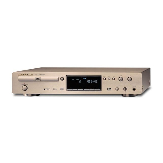
DVD PLAYER DV7000
OPEN/CLOSE
V I D E O
STANDBY
POWER
ON/OFF
SURROUND
TABLE OF CONTENTS
DV7000
DV7000 /
DIMMER
A-B
REPEAT
SHUFFLE
SVCD
SCAN
CHAPTER
TITLE
TRACK
TITLE
DTS
CHAPTER
TRACK
PBC
FTS
TOTAL
TRACK
TIME
PAUSE
SHUFFLE
SCAN
F1N, /K1G, /S1G, /U1G
F1B, /K1B, /N1B, /U1B
DVD Player
STOP
PLAY
LEVEL
PHONES
-
+
PAGE
383K855010 MIT
3120 785 22300
First Issue 2000.07
R
Advertisement

Related Manuals for Marantz DV7000


Summary of Contents for Marantz DV7000
- Page 1 1.13 PARTS LOCATION ........................... 1-27 1.14 EXPLODED VIEW AND PARTS LIST ....................1-32 1.15 ELECTRICAL PARTS LIST ....................... 1-35 2. TKM1000MZ ( DVD MODULE for MARANTZ ) 2.1 SCHEMATIC DIAGRAM AND PARTS LOCATION ................2-1 2.2 MICROPROCESSOR AND IC DATA ....................2-15 2.3 EXPLODED VIEW AND PARTS LIST ....................
- Page 2 MARANTZ Parts for your equipment are generally available to our National Marantz Subsidiary or Agent. ORDERING PARTS : Parts can be ordered either by mail or by Fax.. In both cases, the correct part number has to be specified.
-
Page 3: Technical Specifications
1. TECHNICAL SPECIFICATIONS Discs played DVD video disc ..........12 cm single sided, single layer 12 cm single sided, double layer 12 cm double sided, single layer 12 cm double sided, double layer (one layer per side) 8 cm single sided, single layer 8 cm single sided, double layer 8 cm double sided, single layer 8 cm double sided, double layer (one layer per side) -
Page 4: Connection Facilities
2. CONNECTION FACILITIES Video performance (/N1 only) 1 3 5 7 9 11 13 15 17 19 2 4 6 8 10 12 14 16 18 20 2. 1. 1 SCART Pin No. TV (OUT) Pin No. AUX (IN) Pin 1 Audio R out : 2Vrms Pin 1 Audio R out : 2Vrms... - Page 5 Cancelling password for parental press the DIMMER button /UXX USA/CANADA and hold for 10 seconds while the player is stopped. THE DISCS THAT THE DV7000 CAN HANDLE The following discs can be played back with a DV7000. disc mark playback capability size...
- Page 6 4. SERVICING HINT SERVICE HINTS SERVICE TOOLS Audio signals disc 4822 397 30184 Disc without errors (SBC444)+ Disc with DO errors, black spots and fingerprints (SBC444A) 4822 397 30245 Disc (65 min 1kHz) without no pause 4822 397 30155 Max. diameter disc (58.0 mm) 4822 397 60141 Torx screwdrivers Set (straight)
- Page 7 5. DISASSEMBLY 1. Open the tray and remove the escutcheon (050B). REMARK : If the tray doesn't work, put a small screwdriver into the hole as shown in picture and slide the knob. Then the tray comes out. After the first centimeter it is possible to pull the tray out by hand.
- Page 8 6. REPLACEMENT OF PRINCIPAL COMPONENTS 6-1-2. Removal of the TRAVERSE MECHA. 6-1. Removal of the TRAVERSE MECHA. 1) Remove the four b screws on the MAIN PCB and then 6-1-1. Removal of the MECHANISM BLOCK disconnect the P800 connector on the MAIN PCB. 1) Turn the unit s power on and press the "EJECT"...
- Page 9 3) Carefully disconnect the two connectors (P500, P600) and 6-3. Replacement of the PICK UP BLOCK the two flat cables (P200, P300) on the MECHANISM PCB. Replacement of the PICK UP BLOCK itself is not recommended because its azimuth adjustment is very critical and requires a special jig.
- Page 10 7. SERVICE MODE FLD, LED TEST 1. Press the mains switch (POWER BUTTON) while depressing the PAUSE button and STOP button. 2. Status will be on the TEST mode 1 and FL display shows <TEST 1>. 3. Press the NEXT button, then Standby LED will be light ON and FLD shows <LED 1>.
- Page 11 Type version confirmation 1. Power ON the DVD player. The FL display must be shown <NO DISC>. 2. Pressing the button and button simultaneously. 3. FL display shows product versions as follows. DISPLAY VERSIONS [ USA ] /U1B, /U1G EUROPE /N1B, /N1G [ HK S ‘PORE ]...
-
Page 12: Electrical Adjustment
8. ELECTRICAL ADJUSTMENT VR120 P800 P804 P803 TP120 TP105 TP107 VR121 TP300 VR110 JITTER ADJ JITTER ADJ SCREW A SCREW B VR202 Fig. 8-1 8-1. DVD JITTER ADJUSTMENT 2. Set the oscilloscope to the DC input mode and connect it to 1. - Page 13 8-4 AS Adjustment CAUTION : Do not see the laser pick-up! Cover the laser pick-up unit while AS adjustment. Adjustment point : VR120, VR121 Test point : TP107(+), TP120 (+) TP105 (GND) Equipment : Digital Multi Meter (DC voltage) 1. Press the mains switch (POWER BUTTON) while depressing the PLAY button and STOP button.
- Page 14 9. WAVEFORM Power requirements (Refer the circuit diagram page 1-25 and 1-26) 100V AC 120V AV 220V AC 5µsec 5µsec 100V 5µsec 5µsec 5µsec 5µsec 5µsec 5µsec 5µsec 0.1V 5µsec 0.1V 5µsec 0.1V 5µsec 1-12...
- Page 15 1.10 WARNINGS 1-13 1-14...
- Page 16 1.11 BLOCK DIAGRAM 1-15 1-16...
- Page 17 1.12 SCHEMATIC DIAGRAM AND PARTS LOCATION 1-17 1-18...
- Page 18 1-19 1-20...
- Page 19 FB SWITCH FBIN_ENC FBOUT_TV FBIN_VCR (see Note 1) RGB SWITCH B_ENC B_ENC BOUT_TV BIN_ENC B_VCR G_ ENC BIN_VCR G_ VCR GOUT_TV R/ C _ENC (see Note 1) R_ VCR MUTE GIN_ENC RCOUT_TV GIN_VCR C SWI TCH R/ C _ENC (see Note 1) C_ ENC C_ VCR VOUT_RF...
- Page 20 REPEAT SHUFFLE SCAN CHAPTER TITLE TRACK TITLE CHAPTER TRACK TOTAL TRACK TIME 1-23 1-24...
- Page 21 1-25 1-26...
- Page 22 1.13 PARTS LOCATION PL01 PF01 QF08 QF11 QF01 QF06 QF07 QF05 QF10 QF04 QF09 QF03 QF02 QF12 PK01 QK03 QK05 QK01 QK04 QK06 PP01 PS01 QP05 QP07 QP03 QP18 QP19 QP01 QP04 QP12 QP14 QP13 QP09 QP08 QP06 QP20 - QP22 QP02 QP25 QP24 QP13...
- Page 23 QS04 QS02 QS01 QS03 QS05 QS07 QV12 QH02 - QH12 QH03 - QH11 QV10 QV05 QV08 QV15 (Even number) (Odd number) QV03 QV02 QV07 QV06 QV09 QV10 QV16 QV13 QV17 QV18 QS08 QS09 QS14 QS12 QS15 - QS18 QS11 QS13 QV04 QV11 QV14...
- Page 24 383K105020 002B GOLD 9965 000 05017 FRONT CHASSIS PL(R)GLD 383K105120 Q952 - Q955 Q808 003B BLACK 9965 000 05018 FRONT PANEL AL DV7000 BL 383K248010 Q809 Q960-Q962 003B GOLD 9965 000 05019 FRONT PANEL AL DV7000 GL 383K248110 Q801 005B BLACK 9965 000 05020 BUTTON FUNCTION BLK...
- Page 25 N V E R S I ON 5 1 2 7 5 1 1 0 3 x 8 ( M) 3 x 6 ( M) 5 1 2 6 PA RT S NA ME MA RK MA T E RI A L / F I N I S H SY MB OL S T Y L E 3 X 8 ( M)
- Page 26 1.15 ELECTRICAL PARTS LIST POS. VERS. PART NO. POS. VERS. PART NO. PART NO. PART NO. DESCRIPTION DESCRIPTION ASSIGNMENT OF COMMON PARTS CODES. NOTE ON SAFETY FOR FUSIBLE RESISTOR : COLOR (FOR PCS) COLOR (FOR PCS) (MJI) (MJI) RESISTORS The suppliers and their type numbers of fusible resistors : 1) GD05 ×...
- Page 27 VERS. PART NO. VERS. POS. POS. PART NO. PART NO. PART NO. DESCRIPTION DESCRIPTION COLOR (FOR PCS) COLOR (FOR PCS) (MJI) (MJI) R883 /N 4822 051 30471 CHIP 470Ω ±5% 1/16W NN05471610 D810 /N 4822 130 80346 CHIP DIODE 02CZ8.2 HZ30004050 R884 /N 4822 117 12925 CHIP 47kΩ...
- Page 28 VERS. PART NO. VERS. POS. POS. PART NO. PART NO. PART NO. DESCRIPTION DESCRIPTION COLOR (FOR PCS) COLOR (FOR PCS) (MJI) (MJI) PF01-FRONT CIRCUIT BOARD RF51 4822 051 30103 CHIP 10kΩ ±5% 1/16W NN05103610 PF01-CAPACITORS RF52 4822 051 30152 CHIP 1.5kΩ ±5% 1/16W NN05152610 CF01 RF53...
- Page 29 VERS. VERS. POS. PART NO. POS. PART NO. PART NO. PART NO. DESCRIPTION DESCRIPTION COLOR COLOR (FOR PCS) (FOR PCS) (MJI) (MJI) RK10 4822 051 30151 CHIP 150Ω ±5% 1/16W NN05151610 CP25 9965 000 01318 ELECT. 220µF M 10V RA-2 OA22701020 RK11 4822 051 30222 CHIP 2.2kΩ...
- Page 30 VERS. VERS. POS. PART NO. POS. PART NO. PART NO. PART NO. DESCRIPTION DESCRIPTION COLOR COLOR (FOR PCS) (FOR PCS) (MJI) (MJI) RP52 4822 051 30223 CHIP 22kΩ ±5% 1/16W NN05223610 QP21 4822 130 42715 TRS. A1048.A933S.A1267.ETC. HT10001000 RP53 4822 051 30103 CHIP 10kΩ ±5% 1/16W NN05103610 QP22 4822 130 61189 DIG.TRS.
- Page 31 VERS. PART NO. VERS. POS. POS. PART NO. PART NO. PART NO. DESCRIPTION DESCRIPTION COLOR (FOR PCS) COLOR (FOR PCS) (MJI) (MJI) CS03 4822 124 12404 ELECT. 220µF M 16V RA- 2 OA22701620 CV20 4822 122 33777 CER. CHIP 47pF ±5% CG 50V DD95470300 CS04 4822 124 12404 ELECT.
- Page 32 VERS. VERS. POS. PART NO. POS. PART NO. PART NO. PART NO. DESCRIPTION DESCRIPTION COLOR COLOR (FOR PCS) (FOR PCS) (MJI) (MJI) CV68 /F, /K 5322 124 21731 ELECT. 10µF M 50V RA-2 OA10605020 4822 116 90503 CHIP 150Ω ±5% 1/10W NI05151110 /S, /U RS28...
- Page 33 VERS. PART NO. VERS. POS. POS. PART NO. PART NO. PART NO. DESCRIPTION DESCRIPTION COLOR (FOR PCS) COLOR (FOR PCS) (MJI) (MJI) RV43 /F, /K 4822 051 30471 CHIP 470Ω ±5% 1/16W NN05471610 QH02 4822 130 42839 F.E.T. 2SK369 BL HF203691B0 /S, /U VDGS-40V PDO.4W...
- Page 34 VERS. PART NO. POS. PART NO. DESCRIPTION COLOR (FOR PCS) (MJI) PV01-MISCELLANEOUS FS01 4822 157 10416 EMIFILTER BLM11B102S FN31010030 FS06 FV01 9965 000 05005 FERRITE BEADS FC90020120 FV05 9965 000 05 005 BK1608HM102-T FV06 9965 000 04998 EMI FILTER NFM41R01C221 FM31221020 FV09 FV10...
- Page 35 TKM1000MZ Manual DVD Module for MARANTZ <<IMPORTANT NOTICE>> This service manual explains the product DV7000 which mounted the DVD module TKM1000MZ with the main board <C3M1> only. Products which mounted <C3M1> has product serial number MZ01XXXXXXXXXX. All other products have mounted <M3C1>...
-
Page 37: Schematic Diagram And Parts Location
2.1 SCHEMATIC DIAGRAM AND PARTS LOCATION Not for DV4000... - Page 39 Not for DV4000...
- Page 40 MAIN TOP VIEW TR113 TR115 TR802 TR801 TR100 ~TR106 IC122 IC121 IC120 TR804 ~TR806 TR300 IC507 IC503 TR500 IC111 TR120 TR201 TR202 TR190 IC202 IC203 TR200 IC311 IC607 IC610 ~IC613 IC502 IC702 IC501...
- Page 41 IC911 MAIN BOTTOM VIEW IC701 IC851 IC606 IC850 IC801 IC901 IC802 IC991 IC971 TR114 IC600 IC700 IC703 IC602 IC605 IC800 IC803 TR112 IC110 IC951 TR111 IC500 IC550 IC614 IC852 TR490 TR491 IC490 TR600 IC603 IC300 IC201 TR117 TR167 IC100 TR170 ~TR712 IC931 TR110 TR125...
- Page 42 2-11 2-12...
- Page 43 MECHA TOP VIEW MECHA BOTTOM VIEW TR34 TR90 TR37 TR35 TR36 TR32 TR31 TR33 LOADING MT100 2-13 2-14...
-
Page 44: Microprocessor And Ic Data
2.2 MICROPROCESSOR AND IC DATA CYC11AP000 (DVD Pre AMP) ADV7172 (Video signal decoder) 2-15 2-16... - Page 45 CYC12MP000(DVD Read Channel) 2-17...
- Page 46 MB90574 (CPU/System control MI-COM) Pin No. Port Name FUNCTION System bus read strobe signal output. System bus lower 8 bit write strobe signal output. BOOT Ziva MI-COM transmission control output. CDLOW Disc judge output. LD.SW1 Laser control output 1. System bus ready input. LD.SW2 Laser control output 2.
- Page 47 Pin No. Port Name FUNCTION AVRTM ECC interruption request input (end of output stream of 2060 bytes data) . 68,69 DGND Ð Ground for digital section. SDA(I2C) Serial data in/out from/to EEP-ROM & video encoder. Serial clock output to the EEP-ROM & video encoder. STAT CD-DSP status input.
- Page 48 MN66261 (CD signal processing) 2-20...
- Page 49 MN66261 (CD signal processing) 2-21...
- Page 50 MN67700 (Servo processing IC) 2-22...
- Page 51 MN67700 (Servo processing IC) 2-23...
- Page 52 YMC13D000 (DVD Sync/ECC/Formatter) Pin No. Port Name FUNCTION 1,12,26,35,46, 52,63,73,81, 95,105,118, VSS1-18 Ð Ground pins. 131,142,156, 170,182,195 SEL0 Ð Test mode select pins. SEL1 4-6,8,10,10 11,14-22,28 29,116,117 119,125,126 TEST9-46 Ð Test mode output pins. (Leave them open) 132,171-174 194,197-206 AVRTM End of output stream of 2060 bytes data to CSS.
- Page 53 Pin No. Port Name FUNCTION 127-130 133-139 CPUADT0-15 CPU address/data bus. 143-147 XRESET Global reset input. 148-152 CPUADT16-20 CPU address bus. XALE Address latch enable input. Read strobe. XINTO ECC interrupt request. XWEH Write strobe signal. XWAIT CPU wait state control. XHSTCS Decipher chip select.
- Page 54 ZIVA-3 (Advanced DVD decoder with integrated Audio DSP) Pin No. Port Name FUNCTION 1,52,129 133,138,141 PIO0-10 Programmable I/O pins. 147,153,156 174,190 2-4,6,8-11 HDATA0-7 8 bit bi-directional host data bus. 5,12,17,27 36,40,47,55 61,65,69,75 81,87,91.95 VDD1-29 Ð +3.3 V power supply pins. 101,107,113 117,123,134 149,160,181...
- Page 55 Pin No. Port Name FUNCTION DA-LRCK PCM left/right clock. Identifies the channel for each audio sample. DA-BCK PCM bit clock output. DA-XCK Audio master frequency clock. DAI-DATA PCM input DATA (not used). DAI-LRCK PCM input LRCK (not used). DAI-BCK PCM input BCK (not used). CLKSEL Clock select pin.
-
Page 56: Exploded View And Parts List
2.3 EXPLODED VIEW AND PARTS LIST (TKM1000MZ) 2-28... - Page 57 (VERS. :VERSION, U:U.S.A., F:JAPAN, K:FAR EAST, ** :EUROPE) VERS. POS. PART NO. PART NO. DESCRIPTION COLOR (FOR PCS) (MJI) 9965 000 04593 PLATE CLAMP 294W051010 9965 000 04594 MAGNET 294W012010 9965 000 04595 DISC CLAMP 294W005010 ST PAN26X06STL CMT PT PAN20X05STL CMT C060 9965 000 04596 GEAR LOAD 2 294W058010 9965 000 04597 SLIDER UD...
-
Page 58: Electrical Parts List
2.4 ELECTRICAL PARTS LIST (TKM1000MZ) NOTE ON SAFETY FOR FUSIBLE RESIST OR : ASSIGNMENT OF COMMON P ARTS CODES. RESISTORS The suppliers and their type numbers of fusible resistors are as 1) GD05 x x x 140, Carbon film fixed resistor, 5% 1/4W follows ;... - Page 59 (VERS. :VERSION, U:U.S.A., F:JAPAN, K:FAR EAST, ** :EUROPE) POS. VERS. PART NO. POS. VERS. PART NO. PART NO. PART NO. DESCRIPTION DESCRIPTION COLOR (FOR PCS) COLOR (FOR PCS) (MJI) (MJI) MAIN CIRCUIT BOARD TR106 9965 000 04651 UMG4N BA21711000 DIODES TR110 4822 130 63618 FET 2SK880 HY208802B0...
Need help?
Do you have a question about the DV7000 and is the answer not in the manual?
Questions and answers