Table of Contents
Advertisement
Quick Links
Advertisement
Table of Contents

Related Manuals for Daewoo DSL-20D3


Summary of Contents for Daewoo DSL-20D3
-
Page 1: Service Manual
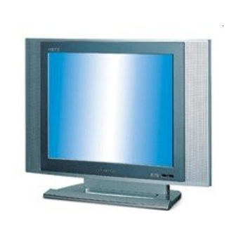
SERVICE MANUAL LCD Television CHASSIS : SL-110P Model : DSL-20D3 APR. 2005... -
Page 2: Table Of Contents
Contents I. Parts with the exception of MODULE 1. Safety Precaution 2. Product Specification 3. Block Diagram 3-1 PCB Structure 3-2 Power Tree 3-3 Signal Block Diagram 4. Description of video circuit 5. Schematic Diagram 6. SL-110P Service Data 7. Service Part List 7-1 Difference List of SL-110P 8. -
Page 3: Safety Precaution
1. Safety Precautions 1. Safety Precautions (1) When moving or laying down a LCD Set, at least two people must work together. Avoid any impact towards the LCD Set. (2) Do not leave a broken LCD Set on for a long time. To prevent any further damages, after checking the condition of the broken Set, make sure to turn the power (AC) off. -
Page 4: Product Specification
2. Product Specification 2-1. SPECIFICATION Model DSL-20D3 CHASSIS NO SL-110P Country Europe Remote controller R-47B02 LCD Panel LCD Type TN (AIO) Screen Size 20” (50.8 Aspect Ratio 4 : 3 Resolution 600 (SVGA) Pixel Pitch 0.51 0.51 Brightness 500 cd/... - Page 5 Product Specification Other Features Comb Filter 17 Languages TELETEXT 10 Page memory TOP / FLOF Audio Output 5W (2.5+2.5W) (10%THD, 60%MOD at 1kHZ) Speaker Aspect ratio control 16 : 9 / ZOOM Auto Power off Wake up Sleep time 15/30/45/60/90/120 min Wall mount hole VESA compatible Power Consumption...
- Page 6 Product Specification 2-2. Available Input Signal (1) PC input Stamdard Resolution (Mode) V Frequency (Hz) H frequency (KHz) 15 inch 17 inch 20inch 832 624 49.73 (2) Component input - 480i/ 60 Hz - 480p / 60 Hz - 576i / 50 Hz - 576p / 50 Hz - 720p / 60 Hz - 1080i / 50 Hz...
-
Page 9: Block Diagram
3-3. SIGNAL BLOCK DIAGRAM SCL1 SDA1 SCL1 SDA1 MAIN IC VCTI FLASH (IC29) SST39VF800A (IC11) LOGIC IC MICOM TUNER PROCESS FILTER (5- Line) 74LV273 (IC40) SCAL ER CVBS EEPROM SCL2 TTX& PW113 (IC13) Vide o In pu t MICOM VIDEO SDA2 24LC16 (IC38) CAPTION... - Page 10 4. Description of video circuit SL-110P video circuit : Process various input signals <Analog-TV signal, CVBS(NTSC), Y/C signal, Component signal(Y-Pb-Pr 1080i, 720P, 480P, 480i), Analog-PC signal> to produce Output Signal for LCD panel(15” : 1024 768, 17” : 1280 768, 20” : 800 600).
- Page 11 Description of video circuit 1) DRX Overview of DRX The Digital Receiver Front-end (DRX) performs the entire multi-standard Quasi Split Sound (QSS) TV IF processing, AGC, video demodulation, and generation of the second sound IF (SIF) requiring only one SAW filter. All control functions and status registers are accessible via I2C bus interface.
- Page 12 Description of video circuit 2) MSP Overview of MSP The MSP receives the digital Sound IF signal from the DRX part. The MSP is able to demodulate all TV sound standards worldwide including the digital NICAM system. INPUT : SIF(DRX) MSP of VCTI Audio signal(External device) CD4052(IC33, Switching)
- Page 13 Description of video circuit 3) VSP Overview of VSP INPUT : CVBS(DRX) VSP of VCTI Video signal(External device) 51& 52 & 53 pin of VCTI(IC29) VSP of VCTI OUTPUT : YUV(4:2:2 or 4:4:4) Features - multi-standard color decoder PAL/NTSC/SECAM including all substandards - macro-vision compliant multi-standard sync processing - macro-vision detection - letterbox detector (auto-wide)
- Page 14 Description of video circuit 4) DDP Overview of DDP The DDP contains the entire digital video component and deflection processing, as well as all analog interfaces to display the picture on a CRT INPUT : YUV(4:4:4 , VSP) DDP of VCTI OUTPUT : 16&...
- Page 15 Description of video circuit 5) TVT Overview of TVT TVT of VCTI UART PW113(IC13) The TVT is a Teletext decoder for decoding World System Teletext data, as well as Video Programming System (VPS), Program Delivery Control (PDC), and Wide-Screen Signalling (WSS) data used for PALplus transmissions.
- Page 16 Description of video circuit 4-2. IC25 and IC30 (TDA1517) : Class-B dual audio amplifier INPUT : Audio signal (84 & 85 pin of VCTI) TDA1517 OUTPUT : Audio signal (TDA1517, amplify) Speaker 4-3. IC16 (MST9883) : Triple Video A/D Converter with Clamps & Pixel Clock Synthesizer INPUT : 1-RF, 1-CVBS, 1-Y/C, 2-Component, 1-PC signal PI5V330(IC5,9,34),Switching...
- Page 17 Description of video circuit 4-4. IC22 (MDIN150) : Single chip of de-interlacing and format conversion. Interlace signal MDIN150, Progressive signal PW113(IC13) Main Features - Performs high quality deinterlacing for arbitrary format of interlaced video input up to 1080i - Motion adaptive 3-D deinterlacing with pixel-by-pixel motion adaptive interpolation - High quality edge preserving deinterlacing thru multiple directional edge detection and interpolation - Deinterlacing with fast motion detection and processing...
- Page 18 Description of video circuit “rocess MDIN output signal to produce Signal for LCD panel(15”± : 1024*768, 17”± : 1280*768, 20”± : 800*600 ). Control : MST9883 and MDIN < I2C > 74LV273A(IC40) <Digital port> Switching IC Features - ITU-R 656 Video Interface - 2nd Generation Horizontal and Vertical Image Scaling - Pixel Rate Conversion - Multi-Region Non-Linear Scaling...
- Page 19 Description of video circuit 4-6. IC17 (EL-LV385) : LVDS Transmitter 24-Bit Flat Panel Display (FPD) Link-85 MHz Output signal of PW113 LV385 (Converting LVDS signal) LCD panel EL-LV385 Transmitter converts parallel 28bits CMOS/TTL data to serial LVDS(Low Voltage Differential Signaling) 4-7.
-
Page 29: Sl-110P Service Data
6. SL-110P Service Data 6-1. SL-110P SERVICE DATA 1. HEATRUN ITEM : SVC remote controller 1) SCV key 2) H/R key : Heatrun 3) H/R key : Heatrun 4) H/R key : Heatrun 5) SCV key : cancel 2. I2C STOP ITEM : SVC remote controller 1) SVC key 2) S.STOP key : BUS STOP 3) S.SOTP key : BUS STOP... - Page 30 SL-110P Service Data 6-2. SL-110P USER_SVC DATA 1. CH MEMORY CONTENTS (Channel data after TV RESET) -- GUMI factory PR. NO SYS. Frequency PATTERN remark PAL-B 40CH 623.25 MHZ PAL-B 48.25 MHZ RETMA PAL-B 175.25 MHZ CROSS HATCH PAL-B 10CH 210.25 MHZ COLOR BAR PAL-B...
- Page 31 SL-110P Service Data 3. USER_SVC Mode (NORMAL 1,2 MODE) : USER_SVC Mode : PR91 Sharpness 0 MENU NORMAL (User remote controller) NORMAL 1 NORMAL 2 NORMAL 1 NORMAL 2 NORMAL 1 NORMAL 2 CONTRAST BRIGHTNESS COLOUR SHARPNESS BRIGHTNESS_PC CONTRAST_PC SHARPNESS_PC 4.
- Page 32 SL-110P Service Data 6-3. SL-110P MASTER IC EXCHANGING METHOD 1. After exchange EEPROM(IC31), Turn the SET on and wait for 20 sec. 2. Confirm LED Blinking and turn the SET on. 3. TV RESET : Method (USER remote controller) 1) PR91 Sharpness 0 MENU SLEEP...
- Page 33 SL-110P Service Data 6-4. Adjusting White Balance 1. More than 30 minutes, heat-run the set in full-white mode whit H/R button of SVC remote controller. 2. Apply HIGH/LOW PATTERN of WHITE BALANCE TESTER (NITSUKI 2849) to Video input terminal (CROMA : OFF, Reference : G) 100% High Level...
- Page 34 SL-110P Service Data 6-5. COMPONENT and PC Test (1) COMPONENT MODE PCB LINE : - Resolution : 480i or 720p - PATTERN : COLOR BAR Finish LINE : - Resolution : 1080i/60Hz - PATTREN : COLOR BAR (2) PC MODE PCB LINE : - Resolution : 800 600 (SVGA VESA 72Hz)
- Page 35 SL-110P Service Data 6-6. PANEL DEFECT Test Visual Inspection 15” SS panel 17” SS panel 20.1” AUO panel diameter <= 0.8 . diameter <= 0.8 . diameter <= 0.5 . Bright Spot Numberr <= 4. Numberr <= 4. Numberr <= 5. diameter <= 0.8 .
-
Page 36: Service Part List
7. Service part list PART CODE PART NAME DESCRIPTION REMARK PART CODE PART NAME DESCRIPTION REMARK ADT1 4859000840 ADAPTER AP06312 C110 HCFF334ZBA C CHIP CERA 16V Y5V 0.33MF Z 1608 M124 485A101470 SHIELDRON 30X140X7.5T C111 HCBK104KBA C CHIP CERA 50V X7R 0.1MF K 1608 M125 485A101470 SHIELDRON... - Page 37 Service part list PART CODE PART NAME DESCRIPTION REMARK PART CODE PART NAME DESCRIPTION REMARK C223 HCBK104KBA C CHIP CERA 50V X7R 0.1MF K 1608 parts_code parts_name parts_descr C228 HCBK102KBA C CHIP CERA 50V X7R 1000PF K 1608 HCBK104KBA C CHIP CERA 50V X7R 0.1MF K 1608 C229 HCBK102KBA...
- Page 38 Service part list PART CODE PART NAME DESCRIPTION REMARK PART CODE PART NAME DESCRIPTION REMARK DZ02W5R6VA DIODE CHIP ZENER Z02W5.6V R247 HRFT152JBA R CHIP 1/10 1.5K OHM J 1608 DZ02W5R6VA DIODE CHIP ZENER Z02W5.6V R248 HRFT152JBA R CHIP 1/10 1.5K OHM J 1608 DZ02W5R6VA DIODE CHIP ZENER Z02W5.6V...
- Page 39 Service part list PART CODE PART NAME DESCRIPTION REMARK PART CODE PART NAME DESCRIPTION REMARK parts_code parts_name parts_descr C260 HCELF470MC C CHIP ELECTRO 16V 47MF CM 5053 HRFT750JBA R CHIP 1/10 75 OHM J 1608 C261 HCBK104KBA C CHIP CERA 50V X7R 0.1MF K 1608 HRFT750JBA R CHIP...
- Page 40 Service part list PART CODE PART NAME DESCRIPTION REMARK PART CODE PART NAME DESCRIPTION REMARK HCBK104KBA C CHIP CERA 50V X7R 0.1MF K 1608 parts_code parts_name parts_descr DZ02W5R6VA DIODE CHIP ZENER Z02W5.6V HLC569K00A L CHIP COIL 5.6UH MLF2012E DM2FM3—-C DIODE CHIP SCHOTTKY M2FM3 M2F TYPE HLC479J00A L CHIP COIL...
- Page 41 Service part list PART CODE PART NAME DESCRIPTION REMARK PART CODE PART NAME DESCRIPTION REMARK 49590009S0 CONN WAFER 12505WR-05A00 HRFT330JBA R CHIP 1/10 33 OHM J 1608 T2N7002M-B FET CHIP 2N7002MTF SOT-23 60V 0.2A R150 HRFT103JBA R CHIP 1/10 10K OHM J 1608 T2SA1037KB TR CHIP 2SA1037AKT146-R...
- Page 42 Service part list PART CODE PART NAME DESCRIPTION REMARK PART CODE PART NAME DESCRIPTION REMARK parts_code parts_name parts_descr RP23 HRTS8E470J R CHIP ARRAY 1/16 8P 47 OHM J 3216 R279 HRFT303JBA R CHIP 1/10 30K OHM J 1608 RP24 HRTS8E470J R CHIP ARRAY 1/16 8P 47 OHM J 3216 R280...
-
Page 43: Difference List Of Sl-110P
Service part list 7-1. Difference List of SL-110P DLP-15D3SHS DLP-17D3SHS DSL-20D3 parts_name parts_desc parts_code Parts_desc parts_code parts_desc Parts_code V901 LCD PANEL LTM150XH-L06 485LD01156 LTM170W1-L01 485LD05171 A201SN02-V0 485LD08200 V902 MODULE DS-1015WDS 4850M001NV DS-1017WDS 4850M008NV DS-1020WDA 4850M004NV INVERTER ADT1 ADAPTER AP06312 4859000840... -
Page 44: Adapter
8. Adapter * Specification Model AP06315-UV SAD7015SE Manufacturing ANAM Instrument H&E Input Voltage AC100~240V 50/60Hz AC100~240V 50/60Hz Output Voltage 15Vdc (14.25~15.75Vdc) 15Vdc (14.5~15.5Vdc) Output Current 0~4.2A 0~4.5A STAND BY Power 3W under 3W under Power Consumption DLP-20D3AHS : 50W DLP-20D3AHS : 50W Over current Protection 5.5~13A 5.0~9.5A... -
Page 45: Inverter
4 Lamp 4 Lamp 6 Lamp (1) Typical Input Voltage : 12V(DLP-15/17D3SHS), 15V(DSL-20D3) (2) Dimming voltage : 0V : MAX BRIGHTNESS 5.0V : Min brightness Fix : 0V (3) Lamp ON/OFF Voltage : HIGH : Inverter ON / Low : Inverter OFF ~ HIGH : BLKON >=3.0V / ~ LOW : BLKON <= 3.0V... - Page 46 Inverter 9-3. Troubleshooting *Backlight doesn’t turn on Ch eck start Is voltage of pin#1,2,3 of P3 and VIN_PWR Check Adapter. 12V(15/17inch)/15V(20inch)? Is voltage of pin#9 Check Main PCB. of P3 over 2.5V? Exchange Inverter or panel. -46-...
Need help?
Do you have a question about the DSL-20D3 and is the answer not in the manual?
Questions and answers