Table of Contents
Advertisement
Quick Links
Advertisement
Table of Contents

Subscribe to Our Youtube Channel
Related Manuals for Icom IC-M710RT


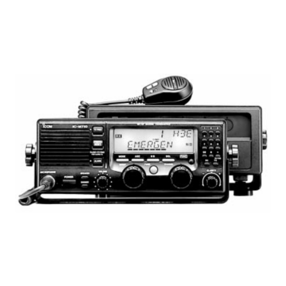
Summary of Contents for Icom IC-M710RT
- Page 1 SERVICE MANUAL MF/HF MARINE TRANSCEIVER iM710RT...
- Page 2 TD62783AF IC-M710RT MAIN UNIT 05 pieces ceiver is defective. 8810009400 Screw PH M3x8 SUS ZK IC-M710RT Rear panel 10 pieces 6. DO NOT transmit power into a signal generator or a sweep generator. Addresses are provided on the inside back cover for your 7.
-
Page 3: Table Of Contents
VR2 BOARD ........................... 8 - 3 8 - 1 - 6 CTRL1 BOARD........................8 - 4 8 - 2 IC-M710RT 8 - 2 - 1 CTRL2 BOARD........................8 - 5 8 - 2 - 2 TERMINAL UNIT ........................8 - 5 8 - 2 - 3 FILTER BOARD ........................ - Page 4 SECTION 1 SPECIFICATIONS ‘ ‘ GENERAL • Frequency coverage : Receive 500 kHz–29.9999 MHz Transmit 1.6000–2.9999 MHz 4.0000–4.9999 MHz 6.0000–6.9999 MHz 8.0000–8.9999 MHz 12.0000–13.9999 MHz 16.0000–17.9999 MHz 18.0000–19.9999 MHz 22.0000–22.9999 MHz 25.0000–27.50000 MHz • Mode : J3E (USB/LSB), H3E (AM), J2B (AFSK), F1B (FSK), R3E, A1A (CW) (Available modes differ with version) •...
- Page 5 SECTION 2 INSIDE VIEWS 50W, FILTER AND TERMINAL BOARDS INAL board amplifiers Q2: 2SC3133) Low-pass filters (FILTER board) al switches Power detector circuit amplifiers Q4: 2SC2904) W board • MAIN AND PLL UNITS RF filter circuit Noise blanker circuit ALARM board 1st mixer circuit MAIN unit 1st IF amplifier...
-
Page 6: Circuit Description
SECTION 3 CIRCUIT DESCRIPTION 3-1 RECEIVER CIRCUITS 3-1-3 2ND MIXER AND IF CIRCUITS (MAIN UNIT) The 1st IF signal from the crystal filter (FI1b) is converted 3-1-1 RF FILTER CIRCUIT (MAIN UNIT) again into a 9.0115 MHz 2nd IF signal at the 2nd mixer cir- Received signals from the antenna connector pass through cuit (D52, L66, L67). - Page 7 AGC detector circuit (D31) and is then applied to the AGC amplifier (Q41) to control the AGC time The PWM signal from the IC-M710RT is applied to the constant line. The reference voltage of the AGC line is con- LOGIC board after being converted into an analog signal by trolled by the “RFG”...
-
Page 8: Transmitter Circuits
3-1-10 SQUELCH CIRCUIT (MAIN UNIT) The AF signals are converted into PWM signal at the PWM modulation circuit (IC3, Q1, D1) via the AF amplifier (CTRL1 The transceiver has two squelch circuits, voice activated board; IC4), and are applied to the serial interface IC (IC1). squelch for J3E/H3E and S-meter squelch for A1A/FSK/J2B. - Page 9 (3) A1A AND FSK MODES 3-2-6 POWER AMPLIFIER CIRCUIT The CW8 or FSK8 voltage are applied to the balanced mod- (PA150W BOARD) ulator (IC9, pin 4) to upset the balance and create a carrier This circuit provides a stable 150 W (at 13.6 V DC) of output signal.
- Page 10 The reference voltage for the comparator is set by R184. (2) CURRENT APC (PA150W BOARD AND MAIN UNIT) The antenna tuning control voltage (TUN8) is also affected The power transistor current is detected from the different voltages between both terminals of a 0.012 Ω resistor (R26) by the reference voltage to decrease the IF signal level.
-
Page 11: Pll Circuits
3-4 PORT ALLOCATIONS 3-3 PLL CIRCUIT 3-4-1 CPU (MAIN unit; IC44) 3-3-1 GENERAL The PLL unit generates a 1st LO frequency (69.5115- Port Description 99.0114 MHz), 2nd LO frequency (60 MHz) and a BFO fre- number name quency (9.0106–9.013 MHz) for the MAIN unit. The 1st LO Input port for the CPU reset signal. - Page 12 (MAIN unit; IC44)–Continued Port Description number name DATA Outputs data to PLL and DDS ICs. Outputs a clock signal to PLL and DDS ICs. Outputs an AF mute signal for squelch SQL C function. High : squelch closed. Outputs an external NBDP equipment control signal.
-
Page 13: Adjustment Procedures
• [MICROPHONE] connector (front view) transmitting. Pin 7 MICE Audio generator Pin 1 MIC IC-M710RT [PTT] Connect pins 3 and 4 for AF output DC power supply 13.6 V/3 A to DC power receptacle [DC 13.6 V]... -
Page 14: Interface Adjustments
4-2 INTERFACE ADJUSTMENTS ADJUSTMENT MEASUREMENT POINT ADJUSTMENT ADJUSTMENT CONDITION VALUE UNIT LOCATION UNIT ADJUST 1 • Connect a main body and controller CTRL2 Connect a frequency 1.2672 MHz CTRL2 INTERFACE ADJUSTMENT with a coaxial cable, then turn counter check power ON. point CP2. -
Page 15: Pll Adjustment
4-3 PLL ADJUSTMENTS ADJUSTMENT MEASUREMENT POINT ADJUSTMENT ADJUSTMENT CONDITION VALUE UNIT LOCATION UNIT ADJUST REFERENCE • Display frequency : 7.9999 MHz Connect digital 3.2 V LOOP LOCK • Mode : J3E multimeter or oscillo- • Receiving scope to check point VOLTAGE •... - Page 16 4-4 TRANSMITTER ADJUSTMENTS ADJUSTMENT MEASUREMENT POINT ADJUSTMENT ADJUSTMENT CONDITION VALUE UNIT LOCATION UNIT ADJUST • Display frequency : 12.2300 MHz PA150W Cut the lead wire 100 mA PA150W IDLING CURRENT • Mode : J3E (W11) and connect a (For drive •...
- Page 17 • PA150W AND FILTER BOARDS Ammeter 7 8 9 DC power supply Idling current (for drive transistors) adjustment Idling current (for final transistors) Idling current adjustment (for drive transistors) check point Ammeter SWR detector Idling current adjustment (for final transistors) check point Ammeter IC APC...
-
Page 18: Transmitter Adjustment
TRANSMITTER ADJUSTMENTS (continued) ADJUSTMENT MEASUREMENT POINT ADJUSTMENT ADJUSTMENT CONDITION VALUE UNIT LOCATION UNIT ADJUST TRANSMIT • Display frequency : 12.2300 MHz Rear Connect 140 W MAIN R184 GAIN • Mode : A1A Panel power meter to the • Transmitting [ANT] connector. •... -
Page 19: Logic Board
• MAIN UNIT L108 R159 Tune power Transmit gain preparation check point R205 Tune power adjustment R883 R184 Mic gain Transmit adjustment gain adjustment R184 R211 R212 Output power adjustment R238 Carrier suppression adjustment • LOGIC BOARD Mic gain adjustment Mic limitter adjustment 4 - 7... - Page 20 4-5 RECEIVER ADJUSTMENTS ADJUSTMENT MEASUREMENT POINT ADJUSTMENT ADJUSTMENT CONDITION VALUE UNIT LOCATION UNIT ADJUST RECEIVER • Display frequency : 2.1820 MHz Rear Connect an AC milli- Muximum output level MAIN Adjust in GAIN • Mode : J3E Panel voltmeter to the [EXT sequence SP] jack with a 4 Ω...
- Page 21 • MAIN UNIT Noise blanker adjustment Noise blanker check point R300 R257 R223 Receiver gain Receiver gain preset adjustment R223 Total gain adjustment 4 - 9...
-
Page 22: Front Unit
SECTION 5 PARTS LIST 5-1 RC-21 [FRONT UNIT] [LOGIC BOARD] ORDER ORDER DESCRIPTION DESCRIPTION 2260001580 SWITCH JPZ2120-0101 (TV-3) 7030000580 S.RESISTOR MCR10EZHJ 47 kΩ (473) 7030000520 S.RESISTOR MCR10EZHJ 15 kΩ (153) 7030000540 S.RESISTOR MCR10EZHJ 22 kΩ (223) 2510000441 SPEAKER F77G08-6205 7030000520 S.RESISTOR MCR10EZHJ 15 kΩ... - Page 23 [LOGIC BOARD] [LOGIC BOARD] ORDER ORDER DESCRIPTION DESCRIPTION 7030000510 S.RESISTOR MCR10EZHJ 12 kΩ (123) 4030004740 S.CERAMIC C2012 JB 1H 472K-T-A 7030000380 S.RESISTOR MCR10EZHJ 1 kΩ (102) 4030004740 S.CERAMIC C2012 JB 1H 472K-T-A 7030000620 S.RESISTOR MCR10EZHJ 100 kΩ (104) 4030004740 S.CERAMIC C2012 JB 1H 472K-T-A 7030000610 S.RESISTOR MCR10EZHJ 82 kΩ...
-
Page 24: Mic Board
[LOGIC BOARD] [VR2 BOARD] ORDER ORDER DESCRIPTION DESCRIPTION 7030000010 S.JUMPER MCR10EZHJ JPW (000) 7210002730 VARIABLE TP96N944-15F-10KB-1632 7030000010 S.JUMPER MCR10EZHJ JPW (000) 7030000010 S.JUMPER MCR10EZHJ JPW (000) 7030000010 S.JUMPER MCR10EZHJ JPW (000) 6510018390 CONNECTOR 06FE-BT-M 7030000010 S.JUMPER MCR10EZHJ JPW (000) 7030000010 S.JUMPER MCR10EZHJ JPW (000) 7030000010 S.JUMPER MCR10EZHJ JPW (000) - Page 25 [CTRL1 BOARD] [CTRL1 BOARD] ORDER ORDER DESCRIPTION DESCRIPTION 7030003440 S.RESISTOR ERJ3GEYJ 102 V (1 kΩ) 4030006860 S.CERAMIC C1608 JB 1H 102K-T-A 7030003440 S.RESISTOR ERJ3GEYJ 102 V (1 kΩ) 4030008880 S.CERAMIC C1608 JB 1C 223K-T-A 7030003640 S.RESISTOR ERJ3GEYJ 473 V (47 kΩ) 4030006860 S.CERAMIC C1608 JB 1H 102K-T-A 7030003640 S.RESISTOR...
-
Page 26: Ic-M710Rt
5-2 IC-M710RT [CTRL2 BOARD] [CONNECT UNIT] ORDER ORDER DESCRIPTION DESCRIPTION 6510007130 CONNECTOR BNC-R111E 7410000950 S.ARRAY EXB-V8V 102JV 6510007130 CONNECTOR BNC-R111E 7030003640 S.RESISTOR ERJ3GEYJ 473 V (47 kΩ) 7030003640 S.RESISTOR ERJ3GEYJ 473 V (47 kΩ) 7030003640 S.RESISTOR ERJ3GEYJ 473 V (47 kΩ) 8600036270 M.OTHER... -
Page 27: Main Unit
[CTRL2 BOARD] [MAIN UNIT] ORDER ORDER DESCRIPTION DESCRIPTION 4030006880 S.CERAMIC C1608 JB 1H 472K-T-A 1160000130 S.IC TD62783AF (TP1) 4030011530 S.CERAMIC C1608 CH 1H 110J-T-A 1160000130 S.IC TD62783AF (TP1) 4030007020 S.CERAMIC C1608 CH 1H 120J-T-A 1160000130 S.IC TD62783AF (TP1) 4610001910 S.TRIMMER CTZ3E-10A-W1 1110003140 IC LA1150N... - Page 28 [MAIN UNIT] [MAIN UNIT] ORDER ORDER DESCRIPTION DESCRIPTION 1540000440 S.TRANSISTOR 2SD1619-T-TD 1750000520 S.DIODE DAN222TL 1540000440 S.TRANSISTOR 2SD1619-T-TD 1790000450 S.DIODE MA862 (TX) 1530002690 S.TRANSISTOR 2SC4116-GR (TE85R) 1790000690 S.DIODE HSM88ASR-TR 1590002120 S.TRANSISTOR UN5211 (TX) 1750000520 S.DIODE DAN222TL 1590002120 S.TRANSISTOR UN5211 (TX) 1790000450 S.DIODE MA862 (TX) 1530002690 S.TRANSISTOR 2SC4116-GR (TE85R)
- Page 29 [MAIN UNIT] [MAIN UNIT] ORDER ORDER DESCRIPTION DESCRIPTION 6140000060 COIL LR-18 6150001590 COIL LS-175 6180002480 COIL LAL 03NA 820K 6200003140 S.COIL NL 322522T-150J 6200002960 S.COIL NL 322522T-4R7J-3 6200003140 S.COIL NL 322522T-150J 6200003100 S.COIL NL 322522T-3R9J-3 6150004430 COIL LS-501 6200003260 S.COIL NL 322522T-101J 6150004300 COIL LS-486A...
- Page 30 [MAIN UNIT] [MAIN UNIT] ORDER ORDER DESCRIPTION DESCRIPTION ELR20J 390 Ω 7010003350 RESISTOR R118 7030003560 S.RESISTOR ERJ3GEYJ 103 V (10 kΩ) ERJ3GEYJ 101 V (100 Ω) 7030003440 S.RESISTOR ERJ3GEYJ 102 V (1 kΩ) R119 7030003320 S.RESISTOR ERJ3GEYJ 181 V (180 Ω) ERJ3GEYJ 101 V (100 Ω) 7030003350 S.RESISTOR R120...
- Page 31 [MAIN UNIT] [MAIN UNIT] ORDER ORDER DESCRIPTION DESCRIPTION R223 7310004080 S.TRIMMER EVM-1YSX50 B53 (502) R329 7030003440 S.RESISTOR ERJ3GEYJ 102 V (1 kΩ) R224 7030003620 S.RESISTOR ERJ3GEYJ 333 V (33 kΩ) R333 7030003480 S.RESISTOR ERJ3GEYJ 222 V (2.2 kΩ) R225 7030003520 S.RESISTOR ERJ3GEYJ 472 V (4.7 kΩ) R334 7030003440 S.RESISTOR...
- Page 32 [MAIN UNIT] [MAIN UNIT] ORDER ORDER DESCRIPTION DESCRIPTION ERJ3GEYJ 101 V (100 Ω) R519 7030003640 S.RESISTOR ERJ3GEYJ 473 V (47 kΩ) R699 7030003320 S.RESISTOR ERJ3GEYJ 821 V (820 Ω) ERJ3GEYJ 101 V (100 Ω) R520 7030003430 S.RESISTOR R700 7030003320 S.RESISTOR ELR20J 5.6 Ω...
- Page 33 [MAIN UNIT] [MAIN UNIT] ORDER ORDER DESCRIPTION DESCRIPTION R825 7030003460 S.RESISTOR ERJ3GEYJ 152 V (1.5 kΩ) 4030009970 S.CERAMIC C1608 JB 1H 182K-T-A R826 7030003520 S.RESISTOR ERJ3GEYJ 472 V (4.7 kΩ) 4030008920 S.CERAMIC C1608 JB 1C 473K-T-A R827 7030003500 S.RESISTOR ERJ3GEYJ 332 V (3.3 kΩ) 4030011600 S.CERAMIC C1608 JB 1C 104KT-N R828...
- Page 34 [MAIN UNIT] [MAIN UNIT] ORDER ORDER DESCRIPTION DESCRIPTION 4030008920 S.CERAMIC C1608 JB 1C 473K-T-A C183 4030007030 S.CERAMIC C1608 CH 1H 150J-T-A 4030006960 S.CERAMIC C1608 CH 1H 050C-T-A C184 4030006990 S.CERAMIC C1608 CH 1H 080D-T-A 4030006860 S.CERAMIC C1608 JB 1H 102K-T-A C185 4030007030 S.CERAMIC C1608 CH 1H 150J-T-A...
- Page 35 [MAIN UNIT] [MAIN UNIT] ORDER ORDER DESCRIPTION DESCRIPTION C276 4030006880 S.CERAMIC C1608 JB 1H 472K-T-A C462 4030006880 S.CERAMIC C1608 JB 1H 472K-T-A C277 4510003940 ELECTROLYTIC 25 MV 4R7 HW C463 4030006860 S.CERAMIC C1608 JB 1H 102K-T-A C278 4510005250 ELECTROLYTIC 50 MV 2R2 SWN C464 4030006880 S.CERAMIC C1608 JB 1H 472K-T-A...
- Page 36 [MAIN UNIT] [MAIN UNIT] ORDER ORDER DESCRIPTION DESCRIPTION C632 4510005260 ELECTROLYTIC 25 MV 10 HW 6510017990 CONNECTOR DELC-J9SAF-20L9 C633 4030008920 S.CERAMIC C1608 JB 1C 473K-T-A 6450001580 CONNECTOR TCS5073-28-4151 C634 4030008920 S.CERAMIC C1608 JB 1C 473K-T-A 6450001590 CONNECTOR TCS5073-17-4151 C637 4030006860 S.CERAMIC C1608 JB 1H 102K-T-A 6510003400 CONNECTOR B04B-EH-S...
-
Page 37: Pll Unit
[PLL UNIT] [PLL UNIT] ORDER ORDER DESCRIPTION DESCRIPTION ERJ3GEYJ 470 V (47 Ω) 1140007880 S.IC SC-1246A 7030003280 S.RESISTOR ERJ3GEYJ 101 V (100 Ω) 1140004550 S.IC SC-1287 7030003320 S.RESISTOR 1180001070 S.IC TA7805F (TE16L) 7030003600 S.RESISTOR ERJ3GEYJ 223 V (22 kΩ) 1130004830 S.IC TC7SU04F (TE85R) 7030003560 S.RESISTOR ERJ3GEYJ 103 V (10 kΩ) - Page 38 [PLL UNIT] [PLL UNIT] ORDER ORDER DESCRIPTION DESCRIPTION ERJ3GEYJ 101 V (100 Ω) 7030003320 S.RESISTOR 4030006860 S.CERAMIC C1608 JB 1H 102K-T-A ERJ3GEYJ 181 V (180 Ω) R100 7030003350 S.RESISTOR 4030006880 S.CERAMIC C1608 JB 1H 472K-T-A ERJ3GEYJ 470 V (47 Ω) R103 7030003280 S.RESISTOR 4510004640 S.ELECTROLYTIC ECEV1CA470SP...
-
Page 39: Pa150W Board
[PLL UNIT] [PA150W BOARD] ORDER ORDER DESCRIPTION DESCRIPTION C135 4030007060 S.CERAMIC C1608 CH 1H 270J-T-A 1110002030 IC TA7808S C136 4030007020 S.CERAMIC C1608 CH 1H 120J-T-A 1110000960 S.IC NJM4558M-T1 C137 4030007060 S.CERAMIC C1608 CH 1H 270J-T-A 1170000290 S.IC PS2701-1-F3 C138 4030006980 S.CERAMIC C1608 CH 1H 070D-T-A 1170000290 S.IC PS2701-1-F3... - Page 40 [PA150W BOARD] [PA150W BOARD] ORDER ORDER DESCRIPTION DESCRIPTION 7010000411 RESISTOR PSN1/4 V 2.2 kΩ 7120000010 JUMPER JPW 02A MCR10EZHJ 470 Ω (471) 7030000340 S.RESISTOR 7120000010 JUMPER JPW 02A MCR10EZHJ 12 Ω (120) 7030000150 S.RESISTOR 7120000010 JUMPER JPW 02A MCR10EZHJ 470 Ω (471) 7030000340 S.RESISTOR 7120000010 JUMPER JPW 02A...
- Page 41 [FILTER BOARD] [FILTER BOARD] ORDER ORDER DESCRIPTION DESCRIPTION 6180000900 COIL LAL 03NA 101K 4010006900 CERAMIC HE80SJ YB 472K 50V 6180000900 COIL LAL 03NA 101K 4010006900 CERAMIC HE80SJ YB 472K 50V 6140002530 COIL LR-291 4010005930 CERAMIC HM11SJ SL 391J 500V 6140001460 COIL LR-170 4010005820 CERAMIC HM74SJ SL 121J 500V...
-
Page 42: Filter Board
[FILTER BOARD] [TERMINAL BOARD] ORDER ORDER DESCRIPTION DESCRIPTION RL15 6330001570 RELAY AJS1315 4510005980 ELECTROLYTIC 16 MV 4700 HC RL16 6330001570 RELAY AJS1315 4010006900 CERAMIC HE80SJ YB 472K 50V RL17 6330000780 RELAY AGP 2013 4010006890 CERAMIC HE60SJ YB 222K 50V 4010006890 CERAMIC HE60SJ YB 222K 50V 4010006900 CERAMIC HE80SJ YB 472K 50V... - Page 43 SECTION 6 MECHANICAL PARTS AND DISASSEMBLY 6-1 RC-21 (CONTROLLER) [FRONT UNIT] [SENSOR1 BOARD] REF. NO. ORDER NO. DESCRIPTION QTY. REF. NO. ORDER NO. DESCRIPTION QTY. 2260001580 JPZ2120-0101 6510018390 Connector 06FE-BT-M 2510000441 F77G08-6205 2250000020 SRB18100 25KC 8900005340 Cable OPC-522 8900005340 Cable OPC-522 [SENSOR2 BOARD] 8900005340 Cable OPC-522...
- Page 44 6-2 IC-M710RT [CHASSIS UNIT] [MAIN UNIT] REF. NO. ORDER NO. DESCRIPTION QTY. REF. NO. ORDER NO. DESCRIPTION QTY. 2710000520 Fan SB0812H-ICOM-00 8510000230 220 shield case 8510000241 220 shield case cover-1 8900006220 Cable OPC-539 8510002200 VCO case 8900006080 Cable OPC-567 8510000230...
- Page 45 MP18 (FR) W4 (R) MP1 (R) MP8 (R) MP10 (R) W3 (R) MP7 (R) W2 (R) MP3 (R) MP27 (FR) W1 (R) MP1 (L) MP4 (R) MP5 (L) CTRL1 BOARD MP6 (L) DS1 (L) MP2 (L) MP2 (R) MP7 (L) MP8 (L) MP3 (L) MP4 (L)
- Page 46 MP17 (CON) J1 (CTRL2) MP15 (CON) MP5 (CON) MP1 (CON) MP4 (CON) MP12 (CON) MP2 (CON) MP3 (CON) MP11 (PA) MP14 (CON) MP13 (CON) MP9 (PA) MP8 (CON) MP6 (CON) J2 (CON) MP35 (PA) W12 (C) EP1 (C) J1 (CON) MP36 (PA) MP3 (C) EP1 (C)
- Page 47 SECTION 7 SEMI-CONDUCTOR INFORMATION • DIODES • TRANSISTOR AND FET’S 1SS184 1SS226 1SS301 1SS302 1SS355 2SA1037K 2SA1213 Y 2SA1586 GR 2SB1015 Y 2SC1623 (Symbol: B3) (Symbol: C3) (Symbol: B3) (Symbol: FR) (Symbol: NY) (Symbol: SG) (Symbol: C3) (Symbol: A) DAN222TL DA221 TL DAN202K DAP202K...
- Page 48 SECTION 8 BOARD LAYOUTS 8-1 RC-21 8-1-1 LOGIC BOARD • TOP VIEW PTTE MICE MISW to MIC board J2 POSW 13-6 to SENSOR1 to SENSOR2 board J1 board J1 to CTRL1 board J4 to CTRL1 board J1 to VR1 to VR2 board J1 board J1 8 - 1...
- Page 49 • BOTTOM VIEW 8 - 2...
-
Page 50: Mic Board
8-1-2 SENSOR 1/2 BOARDS 8-1-3 MIC BOARD PTTE PTTE MICE MICE MISW MISW (UP2) (DN2) to LOGIC to LOGIC board J5 (J6) board J8 8-1-4 VR1 BOARD 8-1-5 VR2 BOARD VOLE VOLE to LOGIC to LOGIC board J4 board J3 8 - 3... - Page 51 8-1-6 CTRL1 BOARD GND2 FTXO FTXO A4RX ESP– A3RX FULD ESP+ FRST A2TX to LOGIC board J10 to CTRL2 board J2 AFG2 AFGE MODE LVDC 13-6 GND1 to LOGIC board J9 8 - 4...
-
Page 52: Ctrl2 Board
8-2 IC-M710RT 8-2-2 TERMINAL UNIT 8-2-1 CTRL2 BOARD PA W3 PA F1 PA F2 • TOP VIEW T/R1 T/R2 F1, F2 to PA150W board to PA150W board AFG2 AFGE to MAIN unit J23 MODE to MAIN unit J16 8 - 5... -
Page 53: Filter Board
to PA150W 8-2-3 FILTER BOARD • BOTTOM VIEW (CTRL 2) board J2 PA UNIT W4 PA UNIT W1, W2 to MAIN unit J2 from ANT connector to MAIN unit J19 8 - 6... - Page 54 8-2-5 ALARM BOARD 8-2-5 ALARM BOARD ALM8 TONE ALMC to MAIN unit J29 to MAIN unit J30 SCAN 13.6 13.6 to REMOTE unit SEND SEND EALC 8-2-4 MAIN BOARD EALC to PLL unit J8 from PA150W AMOD BAND board J1 to CTR2 unit J6 to TERMINAL unit J7...
-
Page 55: Pll Unit
to MAIN unit J9 8-2-6 PLL UNIT MP13 MP11 to MAIN MP12 unit J3 to MAIN unit J5 MP1,MP2 MP17 to MAIN unit J4 8 - 8... -
Page 56: Pa150W Board
to MAIN from unit J22 FILTER 8-2-7 PA150W BOARD board J1 • TOP VIEW PA UNIT MP45 EP10 EP12 to MAIN unit J1 8 - 9... - Page 57 • BOTTOM VIEW 8 - 10...
-
Page 58: Block Diagram
SECTION 9 BLOCK DIAGRAM • RC-21 (CONTROLLER) FRONT UNIT REAR UNIT POWER IC11 TA7805F D8: RD9.1M Q8: 2SD1899 Q11: 2SD1664Q DLC-7978P Q4: 2SC1623 Q5: 2SB1015-Y LAMP V D3: RD9.1M LAMP HD66100F DRIVER Q1: DTC114EKA Q2: DTC114EKA CTRL Q3: DTC114EKA HD6433832SD20F SC-1288 Q2: DTC114EKA Q3: DTC114EKA... - Page 59 • IC-M710RT MAIN UNIT IC8 : LA1150N Q11 : 2SC4116 UN5211 2SC4116 HSM88ASR 2SK210 NOISE NOISE CTRL 2SK2171 RL17 30 MHz FI1a SSB FI2 FL-30 AGP2013 FBR20D12P FL-120 XTAL XTAL GATE 0.5–2 MHz CTRL AM FI3, FI4: FL116 (×2) 1.6 MHz UN5111 89.0115 MHz...
- Page 60 • IC-M710RT SECTION 9 BLOCK DIAGRAM MAIN UNIT IC8 : LA1150N Q11 : 2SC4116 2SK210 UN5211 2SC4116 HSM88ASR NOISE NOISE • RC-21 (CONTROLLER) CTRL 2SK2171 30 MHz RL17 FI1a SSB FI2 FL-30 FBR20D12P AGP2013 FL-120 XTAL XTAL GATE 0.5—2 MHz CTRL AM FI3, FI4: FL116 (×2)
- Page 61 SECTION 10 VOLTAGE DIAGRAM 10kB VOLUME DLC-7978P DTC114EK HRT-3290 HRT-3290 HRT-3290 DIM1 2SC1623 VOLE VOLE DTC114EK 1SS184 VOLE DIM2 VOLE R109 VR1 BOARD DTC114EK 0.01 DIM1 8.3 V DIM3 DIM2 7.4 V 2SB1015 DIM3 6.2 V DIM4 4.4 V 13.6 V 10kB CLARITY HD66100F...
- Page 62 0.2 sec 3.7 Vp-p TC7W74FU GND1 CR-508 1.2k (5.0688 MHz) A2TX A2TX FRST FULO LOGIC A3RX board A4RX FTXO FRXO GND2 optional unit OPC-774 DSA3A1 0.0047 FTXO FK-060C-1020 NJM311M-TE3 DAR1 FRXO DAR2 SC-1288 SIGI FRST SIGO 3.2 V FULO SIGO1 2SA1586 220p CHI1...
- Page 63 SECTION 10 VOLTAGE DIAGRAM 0.2 sec 3.7 Vp-p 10kB TC7W74FU VOLUME DLC-7978P DTC114EK GND1 HRT-3290 HRT-3290 HRT-3290 CR-508 DIM1 A2TX A2TX 1.2k (5.0688 MHz) 2SC1623 FRST VOLE VOLE DTC114EK 1SS184 VOLE DIM2 VOLE FULO LOGIC R109 A3RX VR1 BOARD DTC114EK 0.01 board DIM3...
- Page 64 TERMINAL board PFSK 10 H STB2 R140 STB2 STB1 R141 STB1 CON2 R142 CON2 CON1 R143 CON1 MAIN CON0 R144 CON0 unit DRST R145 DRST STB3 R146 STB3 DATA R147 DATA SG (GND) R148 CI (RI) 13.6 ER (DTR) 13.6 EXC-ELDR25C DS14C232TM 0.3 sec...
- Page 65 TX: 1.5 V 0.0047 100p 2.2k MAIN unit 0.01 LW-25 100 H 100 H TX: 0.65 V R200 1.5k R199 13.6 V PFSK 2SC1971 2SC3133 10 H HVM17 13.6 V STB2 R140 STB2 LC7153M LR-274 LR-143 STB1 R141 STB1 1SS226 CON2 R142 CON2...
- Page 66 TX: 1.5 V TX: 0.65 V 0.0047 100p 2.2k MAIN unit 0.01 300p EXC-ELDR25C AJS1315 AJS1315 TX: 0.65 V FILTER BOARD 13.6 V 0.5 M < 2 MHz LR-236 LR-226 LR-227 RX: 9.6 V PA150W 13.6 V 2SC1971 2SC3133 2SC2904 board J2 13.6 V LR-148...
- Page 67 TX: 1.5 V TX: 0.65 V 0.0047 100p 2.2k 0.01 300p MAIN unit EXC-ELDR25C AJS1315 AJS1315 LW-25 100 H 100 H TX: 0.65 V R200 1.5k 13.6 V 0.5 M < 2 MHz FILTER BOARD TERMINAL LR-236 LR-226 LR-227 board R199 RX: 9.6 V 13.6 V...
- Page 68 TX: 7.9 V L116 L130 from 100 H 100 H LR-18 PA unit 100 H from FILTER 5.6 H 4.7 H 0.047 100 H 560 H 100 H LR-270 LA1150N LS-163A board 0.001 C637 2SK131 0.001 L129 LS-466 100 H 270p MA862 MA862...
- Page 69 L130 100 H DETO C270 L127 IC21 100 H 100 H NJM4558M LA1150N 0.001 IC22b C115 R258 R257 R256 C250 R277 C259 R293 C265 R297 DAN222TL R752 120p 2.2k 220p 100k R306 LS-466 Q131 PRO8 C118 2SC4116 IC20 R753 0.4 V NJM4558M C243 R281...
- Page 70 DETO C270 IC21 R892 6.8k R883 NJM4558M ALARM BOARD R345 (MARINE ONLY) 0.0047 DAN222TL R752 R882 R306 PRO8 Q119 R753 R346 C279 2SC4116 AFG2 DAN222TL 180k R700 Q124 2SC4116 DTC114EU C608 R344 TONE IC38b TONE 0.47 100k R342 1SS302 R757 100k R328 R324...
- Page 71 TX: 7.9 V L116 L130 from 100 H 100 H LR-18 DETO PA unit L127 IC21 C270 R883 R892 6.8k from 100 H 100 H NJM4558M ALARM BOARD FILTER 5.6 H 4.7 H 0.047 100 H 560 H 100 H LR-270 LA1150N R345...
- Page 72 08190 Sant Cugat del Valles Barcelona, SPAIN Phone : ( 93 ) 590 26 70 Fax : ( 93 ) 589 04 46 A Division of Icom America Inc. 3071 #5 Road, Unit 9, Richmond, B.C., V6X 2T4, Canada : http://www.icomspain.com...
- Page 73 A-5504HI-S1 6-9-16, Kamihigashi, Hirano-ku, Osaka 547-0002, Japan C C 1999 Icom Inc.
Need help?
Do you have a question about the IC-M710RT and is the answer not in the manual?
Questions and answers
How to unlock general coverage transmitter frequencies for the M710RT