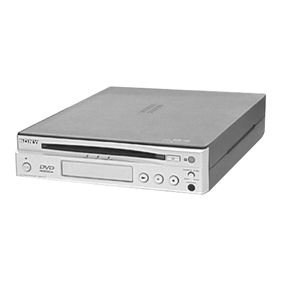
Sony DVP-F11 Service Manual
Cd/dvd player
Hide thumbs
Also See for DVP-F11:
- Operating instructions manual (68 pages) ,
- Service manual (97 pages) ,
- Quick start manual (2 pages)
Table of Contents
Advertisement
Quick Links
SERVICE MANUAL
CD/DVD player
Laser
Semiconductor laser
Signal format system
PAL/(NTSC)
Audio characteristics
Frequency response
DVD (PCM 96 kHz): 2 Hz to 44 kHz
(±1 dB)*
DVD (PCM 48 kHz): 2 Hz to 22 kHz
(±0.5 dB)
CD: 2 Hz to 20 kHz (±0.5 dB)
Signal-to-noise ratio
More than 110 dB (LINE OUT (AUDIO
1, 2) connectors only)
Harmonic distortion
Less than 0.0025%
Dynamic range
More than 100 dB (DVD)
More than 97 dB (CD)
Wow and flutter
Less than detected value
(±0.001% W PEAK)
Outputs and inputs
Jack
Output
type
level
LINE OUT
Phono
2 Vrms
(AUDIO1, 2)
jacks
(at 50 kilohms)
OPTICAL
Optical
–18 dBm
output
connector
COAXIAL
Phono
0.5 Vp-p
jack
LINE OUT
Phono
1.0 Vp-p
(VIDEO1, 2)
jacks
LINE OUT
4-pin
Y: 1.0 Vp-p
(S-VIDEO1, 2)
mini DIN
C: 0.3 Vp-p
(PAL)
0.286 Vp-p
(NTSC)
LINE OUT
Phono
2 Vrms
(WOOFER OUT) jacks
PHONES
Phone
12 mW
jack
MICROFILM
SPECIFICATIONS
General
Power requirements
Power consumption
Dimensions (approx.)
Mass (approx.)
Operating temperature
Operating humidity
AC power adaptor
Power requirements
Power consumption
Output voltage
Dimensions (approx.)
Mass (approx.)
Operating temperature
Storage temperature
Supplied accessories
Load impedance
• Audio/Video connecting cord (1)
• S video cord (1)
Over 10 kilohms
• AC power adaptor AC-F11 (1)
• AC power cord (1)
Wave length: 660 nm
• Remote commander (remote) RMT-D109O (1)
(Except Hong Kong, Singapore and Chinese)
Remote commander (remote) RMT-D109E (1)
75 ohms terminated
(Hong Kong, Singapore and Chinese)
• Size AA (R6) batteries (2)
• Stand (1)
75 ohms,
• EURO AV adaptor (1)
sync negative
(Except Hong Kong, Singapore, Australian and Chinese)
75 ohms,
sync negative
* The signals from LINE OUT (AUDIO1, 2) connectors are measured.
75 ohms terminated
When you play the PCM sound tracks with 96 kHz sampling frequency,
the output signals from the OPTICAL and COAXIAL connectors are
converted to 48 kHz (sampling frequency).
Over 10 kilohms
Design and specifications are subject to change without notice.
32 ohms
DVP-F11
RMT-D109E/D109O
AEP Model
UK Model
E Model
Hong Kong Model
Singapore Model
Australian Model
Chinese Model
DC 10.5 V
13 W
215
60
314 mm (w/h/d)
incl. projecting parts
2.1 kg
5 C to 35 C
25% to 80%
220 to 240 V AC, 50/60 Hz
19 W
DC 10.5 V, 1.3 A in operating mode
125
39
62 mm (w/h/d)
excl. projecting parts
235 g
5 C to 35 C
–20 C to +60 C
CD/DVD PLAYER
Advertisement
Table of Contents

Related Manuals for Sony DVP-F11


Summary of Contents for Sony DVP-F11
- Page 1 DVP-F11 RMT-D109E/D109O SERVICE MANUAL AEP Model UK Model E Model Hong Kong Model Singapore Model Australian Model Chinese Model SPECIFICATIONS CD/DVD player General Power requirements Laser Semiconductor laser DC 10.5 V Signal format system Power consumption 13 W PAL/(NTSC) Dimensions (approx.) 314 mm (w/h/d) incl.
- Page 2 LINE WITH MARK 0 ON THE SCHEMATIC DIAGRAMS AND IN THE PARTS LIST ARE CRITICAL TO SAFE OPERATION. REPLACE THESE COMPONENTS WITH SONY PARTS WHOSE PART NUMBERS APPEAR AS SHOWN IN THIS MANUAL OR IN SUPPLEMENTS PUB- LISHED BY SONY.
-
Page 3: Table Of Contents
TABLE OF CONTENTS Section Title Page Section Title Page Service Note ................4 HP-122 Printed Wiring Board and Schematic Diagram ..........4-55 GENERAL MPD0102 Printed Wiring Board and Schematic Diagram ..........4-57 This Player Can Play the Following Discs ....1-1 IC PIN FUNCTION DESCRIPTION Getting Started .............. -
Page 4: Service Note
SERVICE NOTE 1. DISASSEMBLY • This set can be disassembled in the order shown below. Note on Replacing IC601 (IF CON) (FL-111 Board) There are two types of IC601 (IF CON). Version Type (Part No.) Ver. 1.00 M38B57MCH-E227FP (8-759-599-87) Ver. 1.01 M38B57MCH-D233FP (8-759-658-36) Case (Upper) (Page 2-1) -
Page 5: General
DVP-F11 SECTION 1 This section is extracted from in- GENERAL struction manual (3-867-780-11). - Page 14 1-10...
- Page 15 1-11...
- Page 16 1-12...
- Page 17 1-13...
- Page 18 1-14...
- Page 19 1-15 E 1-15...
-
Page 20: Disassembly
DVP-F11 SECTION 2 DISASSEMBLY Note: Follow the disassembly procedure in the numerical order given. 2-1. CASE (UPPER) REMOVAL 2-3. AU-222 BOARD REMOVAL 4 AU-222 board 2 Remove the case (upper) in the direction of the arrow. 1 Two screws (B3) -
Page 21: Rear Panel, Mb-85 Board Removal
2-5. REAR PANEL, MB-85 BOARD 2-7. FRONT PANEL SECTION REMOVAL REMOVAL 8 Two screws 9 Boss 1 Flat cable 5 Connector (B3) (ring) (CN602) (CN011) 4 Three flat cables 6 Flat cable (CN002, 003, 009) (CN006) 9 MB-85 board 7 Two screws (B3) (ring) 8 Claw 1 Two screws... -
Page 22: Board, Optical Pick-Up Removal
2-9. TK-55 BOARD, OPTICAL PICK-UP 2-11. CAM SLIDER, CHASSIS (FRONT) REMOVAL BLOCK ASS’Y REMOVAL 1 Two screws (B3) 1 Tension spring 4 Remove the cam slider in the 2 Ground plate (MD) (cam slider) direction of the arrow A. 3 Flexible board 7 TK-55 (CN002) board... -
Page 23: Internal Views
2-13. INTERNAL VIEWS Switch (chuck sensor) 1-570-771-21 Optical pick-up (KHM-220AAA/J1RP) LD motor ass’y 8-820-081-09 (loading) A-6062-252-A Harness (ST-117) 1-960-020-11 Optical pick-up (KHM-220AAA/J1RP) 8-820-081-09... -
Page 24: Circuit Boards Location
2-14. CIRCUIT BOARDS LOCATION MB-85 (SIGNAL PROCESS/SERVO) TK-55 AU-222 (RF/SERVO) (AUDIO) FR-166 (IR/FUNCTION SWITCH) DC-DC Converter Unit SW-332 (SWITCHING REGULATOR) (CHUCK SENSOR) FL-111 HP-122 (IF CON) (HEAD PHONE) 2-5 E... -
Page 25: Block Diagrams
DVP-F11 SECTION 3 BLOCK DIAGRAMS 3-1. OVERALL BLOCK DIAGRAM MB-85 BOARD (SEE PAGE 4-19 to 37) IC304 IC402, 403 16M DRAM 16M SDRAM BASE UNIT TK-55 BOARD AU-222 BOARD KHM-220AAA (SEE PAGE 4-11) (SEE PAGE 4-43, 45) VIDEO V, OPTICAL DEVICE... -
Page 26: Rf/Servo Block Diagram
DVP-F11 3-2. RF/SERVO BLOCK DIAGRAM IC0011(DVD play) IC0011(CD play) IC001tf(CD play) IC001r;(CD play) IC001tf(DVD play) IC001r;(DVD play) 500mV/DIV 500ns/DIV 200mV/DIV 100ns/DIV 500mV/DIV 500ns/DIV 500mV/DIV 100ns/DIV 100mV/DIV 50ms/DIV 500mV/DIV 50ms/DIV 536mVp-p 880mVp-p 1.5Vp-p 1.5Vp-p 180mVp-p 860mVp-p IC701yk(CD play) IC701yk(DVD play) IC701yl(DVD play) -
Page 27: Signal Process/Video Block Diagram
DVP-F11 3-3. SIGNAL PROCESS/VIDEO BLOCK DIAGRAM MB-85 BOARD (2/6) (SEE PAGE 4-19, 21, 27, 35) AU-222 BOARD (1/2) (SEE PAGE 4-43, 45) IC303qj(DVD play) 500mV/DIV 100ns/DIV IC304 IC402, 403 16M DRAM 16M SDRAM 1.6Vp-p IC303ql(CD play) 500mV/DIV 200ns/DIV IC308qg 1.6Vp-p 2.0Vp-p(H) -
Page 28: System Control Block Diagram
DVP-F11 3-4. SYSTEM CONTROL BLOCK DIAGRAM EXCEPT CED, UK, Chinese CED, UK, Chinese MB-85 BOARD (3/6) (SEE PAGE 4-29, 31, 33) IC204 IC205 IC206 1M SRAM 16M FLASH 16M FLASH HA 0-21 SIGNAL PROCESS, VIDEO +3.3V IC207 AUDIO 1 (SEE PAGE 3-5) -
Page 29: Audio (1) Block Diagram
DVP-F11 3-5. AUDIO (1) BLOCK DIAGRAM MB-85 BOARD (4/6) (SEE PAGE 4-33, 35) SPDIF IC501 IC902 AUDIO DSP AUDIO 2CH DAC BCKO BCLKIN V OUT L AUDIOLT BCKI LRCK LRCKI LRCKO LRCIN V OUT R AUDIORT ACH12 CH78O D IN... -
Page 30: Audio (2) Block Diagram
DVP-F11 3-6. AUDIO (2) BLOCK DIAGRAM MB-85 BOARD (5/6) (SEE PAGE 4-35) INTERFACE A MUTE CONTROL (SEE PAGE 3-14) AU-222 BOARD (2/2) J301 (SEE PAGE 4-43, 45) MA MUTE Q325 COAXIAL BUFFER VFC2 PCM/DTS/ IC309 VFC1 DOLBY DIGITAL SYSTEM CONTROL... -
Page 31: Interface Control Block Diagram
DVP-F11 3-7. INTERFACE CONTROL BLOCK DIAGRAM FL-111 BOARD FR-166 BOARD MB-85 BOARD (6/6) (SEE PAGE 4-49) (SEE PAGE 4-53) (SEE PAGE 4-29) IC701 REMOTE COMMANDER RECEIVER CN701 CN603 CN602 CN006 SCLK1 IFSC0 SOUT1 IFSI0 IC601 LPOW L POWER IF CON... -
Page 32: Power Block Diagram
DVP-F11 3-8. POWER BLOCK DIAGRAM DC-DC CONVERTER UNIT (MPD0102) AU-222 BOARD (SEE PAGE 4-57) (SEE PAGE 4-43, 45) AC ADAPTOR L202 IC281 (AC-F11) CN303 LINE FILTER EVER+5V REG SW+10V +7.5V J201 CN202 IC303 EVER5V IC301 IC304 +7.5V/–7.5V Q291, 293 SW+10V... -
Page 33: Printed Wiring Boards And Schematic Diagrams
DVP-F11 SECTION 4 PRINTED WIRING BOARDS AND SCHEMATIC DIAGRAMS THIS NOTE IS COMMON FOR PRINTED WIRING For schematic Diagram: • Caution when replacing chip parts. BOARDS AND SCHEMATIC DIAGRAMS. New parts must be attached after removal of chip. (In addition to this, the necessary note is printed Be careful not to heat the minus side of tantalum capacitor, in each block.) -
Page 34: Frame Schematic Diagram
DVP-F11 4-1. FRAME SCHEMATIC DIAGRAM FRAME (1) SCHEMATIC DIAGRAM BASE UNIT KHM-220AAA/J1N CN001 N.C. N.C. CN003 CN002 SSDFCT SSDFCT SSCS SSCS SSRD SSRD SSWD SSWD SSCK SSCK 3.3V FMT-27 3.3V OPTICAL DEVICE VC(2.5V) VC(2.5V) VCC(5V) VCC(5V) SSDFCTI SSDFCTI MIRR MIRR... -
Page 35: Frame (2) Schematic Diagram
DVP-F11 FRAME (2) SCHEMATIC DIAGRAM HP-122 BOARD CN501 CN306 IC309 J301 J303 AH-114 COAX WOOFER OUT J302 AV JACK AU-222 BOARD CN202 CN303 SW-10V SW-10V SW+10V SW+10V PA-127 SW+5V SW+5V EVER5V EVER5V FMA-17 FMA-18 DC-DC CONVERTER UNIT (MPD0102) CN001 CN201 SW+3.3V... -
Page 36: Printed Wiring Boards And Schematic Diagrams
DVP-F11 There are few cases that the part isn't mounted in this model is printed on this diagram. 4-2. PRINTED WIRING BOARDS AND SCHEMATIC DIAGRAMS TK-55 (RF/SERVO) PRINTED WIRING BOARD – Ref. No.: TK-55 board; 2,000 series – TK-55 BOARD (SIDE A) - Page 37 DVP-F11 • Waveforms 1 IC001 1 (DVD play) 6 IC001 el (CD play) 200 mV/DIV 100 ns/DIV 500 mV/DIV 200 ms/DIV 536 mVp-p 1.7 Vp-p 2 IC001 1 (CD play) 7 IC001 r; (DVD play) 100 mV/DIV 50 ms/DIV 500 mV/DIV 500 ns/DIV...
- Page 38 DVP-F11 TK-55 (RF/SERVO) SCHEMATIC DIAGRAM • See page 4-7 for printed wiring board and page 4-10 for waveforms. – Ref. No.: TK-55 board; 2,000 series – TK-55 BOARD CN001 CN003 N.C. C029 C031 DVD/CD 0.1u LD MODULE MIRR MIRR R002...
- Page 39 DVP-F11 SW-332 (CHUCK SENSOR) PRINTED WIRING BOARD AND SCHEMATIC DIAGRAM – Ref. No.: SW-332 board; 2,000 series – There are few cases that the part isn't mounted in this model is printed on this diagram. SW-332 BOARD CN101 JL101 OCSW1...
- Page 40 DVP-F11 MB-85 (SIGNAL PROCESS/SERVO) PRINTED WIRING BOARD There are few cases that the part isn't mounted in this model is printed on this diagram. – Ref. No.: MB-85 board; 1,000 series – MB-85 BOARD (SIDE A) CN001 CN002 CN003 CN005...
- Page 41 DVP-F11 MB-85 BOARD (SIDE B) D701 D806 IC005 IC201 IC203 IC204 IC207 IC304 IC402 IC403 IC404 IC702 IC801 IC802 IC803 IC902 IC907 SIGNAL PROCESS/SERVO MB-85 4-17 4-18...
-
Page 42: Av Decoder) Schematic Diagram
DVP-F11 MB-85 (AV DECODER) SCHEMATIC DIAGRAM • See page 4-15 for printed wiring board. – Ref. No.: MB-85 board; 1,000 series – MB-85 BOARD(1/10) XCS2 MB-85 BOARD(6/10) XCS3 XWRH MB-85 BOARD(6/10) XAVDIT XAVDWT MB-85 BOARD(7/10) DACK0 DREQ0 MB-85 BOARD(6/10) DACK1... -
Page 43: Mb-85 (Sdram) Schematic Diagram
DVP-F11 MB-85 (SDRAM) SCHEMATIC DIAGRAM • See page 4-15 for printed wiring board. – Ref. No.: MB-85 board; 1,000 series – • Waveforms MB-85 BOARD(2/10) 1 IC401 ya 27M30 MB-85 BOARD(8/10) IC402 16M SDRAM FL402 C405 IC402 KM416S1020CT-G10T 0.01u CL477... -
Page 44: Servo Dsp) Schematic Diagram
DVP-F11 MB-85 (SERVO DSP) SCHEMATIC DIAGRAM • See page 4-15 for printed wiring board. – Ref. No.: MB-85 board; 1,000 series – • Waveforms MB-85 BOARD(3/10) 1 IC701 yl (DVD play) TRD+ 500 mV/DIV 50 ms/DIV TRD- MB-85 BOARD(4/10) FCD+... -
Page 45: Drive) Schematic Diagram
DVP-F11 MB-85 (DRIVE) SCHEMATIC DIAGRAM • See page 4-15 for printed wiring board. – Ref. No.: MB-85 board; 1,000 series – MB-85 BOARD(4/10) D802 1SS355TE-17 SPDLSTOP MB-85 BOARD(7/10) R831 D801 DAP202UT106 +3.3V MB-85 BOARD(5/10,6/10) MB-85 BOARD(3/10) FGMODE S10V MB-85 BOARD(10/10) -
Page 46: Arp) Schematic Diagram
DVP-F11 MB-85 (ARP) SCHEMATIC DIAGRAM • See page 4-15 for printed wiring board. – Ref. No.: MB-85 board; 1,000 series – MB-85 BOARD(5/10) • Waveforms FL303 MB-85 BOARD +3.3V (4/10) 1 IC303 qj (DVD play) C321 500 mV/DIV 100 ns/DIV 100u 6.3V... -
Page 47: System Control) Schematic Diagram
DVP-F11 MB-85 (SYSTEM CONTROL) SCHEMATIC DIAGRAM • See page 4-15 for printed wiring board. – Ref. No.: MB-85 board; 1,000 series – MB-85 BOARD(6/10) +3.3V MB-85 BOARD(4/10) XRAMWE IC204 IDT71V016S20PHAU-TL MB-85 BOARD(7/10) IC204 1M SRAM FL204 CL201 MB-85 BOARD(8/10) CKSEL... -
Page 48: Hga) Schematic Diagram
DVP-F11 MB-85 (HGA) SCHEMATIC DIAGRAM • See page 4-15 for printed wiring board. – Ref. No.: MB-85 board; 1,000 series – MB-85 BOARD(7/10) +3.3V MB-85 BOARD(10/10) C601 CPUCK MB-85 BOARD(6/10) XCS1 XCS4 XWRL XWRH MB-85 BOARD(6/10) MB-85 BOARD(6/10) XINT3 XINT1... -
Page 49: Clock Generator/Audio Dsp) Schematic Diagram
DVP-F11 MB-85 (CLOCK GENERATOR/AUDIO DSP) SCHEMATIC DIAGRAM • See page 4-15 for printed wiring board. – Ref. No.: MB-85 board; 1,000 series – MB-85 BOARD(8/10) • Waveforms 1 IC004 2, 5, 7 6 IC001 qf (DVD play) +3.3V MB-85 BOARD(10/10) -
Page 50: Dac) Schematic Diagram
DVP-F11 MB-85 (DAC) SCHEMATIC DIAGRAM • See page 4-15 for printed wiring board. – Ref. No.: MB-85 board; 1,000 series – MB-85 BOARD(9/10) MB-85 BOARD(7/10) XDACRST 384FSDA MB-85 BOARD(8/10) C907 C906 R915 MB-85 BOARD(6/10) 0.1u VIDEOV XDACS0 C905 0.01u VIDEOY... -
Page 51: Mb-85 (Bias) Schematic Diagram
DVP-F11 MB-85 (BIAS) SCHEMATIC DIAGRAM • See page 4-15 for printed wiring board. – Ref. No.: MB-85 board; 1,000 series – MB-85 BOARD(10/10) FL014 FB106 FB105 V3.3V MB-85 BOARD(1/10) C015 CN001 220u FL002 FB001 FB003 CL005 CL028 +3.3V MB-85 BOARD SW+3.3V... - Page 52 DVP-F11 AU-222 (AUDIO/VIDEO BUFFER) PRINTED WIRING BOARD There are few cases that the part isn't mounted in this model is printed on this diagram. – Ref. No.: AU-222 board; 2,000 series – AU-222 BOARD (SIDE A) D301 D304 D305 D306...
- Page 53 DVP-F11 AU-222 BOARD (SIDE B) CN301 CN302 CN303 CN306 D302 D308 D309 D310 D311 IC301 IC303 IC304 IC305 IC307 IC309 IC310 Q302 Q323 Q324 Q330 Q331 Q332 Q333 AUDIO/VIDEO BUFFER AU-222 4-41 4-42...
-
Page 54: Au-222 (Audio) Schematic Diagram
DVP-F11 AU-222 (AUDIO) SCHEMATIC DIAGRAM • See page 4-39 for printed wiring board. – Ref. No.: AU-222 board; 2,000 series – AU-222 BOARD(1/2) VMUTE R471 C301 VIDEOV R396 R399 C322 L301 R366 R370 R302 390p Q321 15uH R400 330k R468 C306 2SD1938(F)-T(TX).SO... -
Page 55: Au-222 (Video Buffer) Schematic Diagram
DVP-F11 AU-222 (VIDEO BUFFER) SCHEMATIC DIAGRAM • See page 4-39 for printed wiring board. – Ref. No.: AU-222 board; 2,000 series – • Waveforms AU-222 BOARD(2/2) 1 IC308 2 6 IC308 qg CN306 FB317 HP-122 BOARD FB318 CN501 FB319 (SEE PAGE 4-55) - Page 56 DVP-F11 FL-111 (IF CON) PRINTED WIRING BOARD – Ref. No.: FL-111 board; 2,000 series – There are few cases that the part isn't mounted in this model is printed on this diagram. FL-111 BOARD (SIDE A) CN602 CN604 D604 D607...
-
Page 57: Schematic Diagram
DVP-F11 FL-111 (IF CON) SCHEMATIC DIAGRAM – Ref. No.: FL-111 board; 2,000 series – FL-111 BOARD ND601 FLUORESCENT INDICATOR TUBE L601 47uH Q604 R603 2SD1622-S-TD 6800 C603 C605 D601 0.1u -0.1 MA113-(TX) JL607 -9.9 -10.2 T601 D604 D606 C601 C630... - Page 58 DVP-F11 There are few cases that the part isn't mounted in this model is printed on this diagram. FR-166 (IR/FUNCTION SWITCH) PRINTED WIRING BOARD – Ref. No.: FR-166 board; 2,000 series – FR-166 BOARD (SIDE B) CN701 D701 D702 D703...
- Page 59 DVP-F11 FR-166 (IR/FUNCTION SWITCH) SCHEMATIC DIAGRAM – Ref. No.: FR-166 board; 2,000 series – FR-166 BOARD R708 R709 R710 R711 R712 R713 R714 CN701 LPLAY LPAUSE D701 SPR-325MVW LVCD (ON/STANDBY) LDVD FL-111 BOARD L701 CN603 22uH R701 (SEE PAGE 4-50)
-
Page 60: Printed Wiring Board And Schematic Diagram
DVP-F11 HP-122 (HEADPHONE) PRINTED WIRING BOARD AND SCHEMATIC DIAGRAM – Ref. No.: HP-122 board; 2,000 series – There are few cases that the part isn't mounted in this model is printed on this diagram. HP-122 BOARD R502 RV501 FB501 PHONES LEVEL... -
Page 61: Mpd0102 Board
DVP-F11 MPD0102 (SWITCHING REGULATOR) PRINTED WIRING BOARD AND SCHEMATIC DIAGRAM There are few cases that the part isn't mounted in this model is printed on this diagram. – Ref. No.: MPD0102 board; 6,000 series – MPD0102 BOARD MPD0102 BOARD CN201... -
Page 62: Ic Pin Function Description
DVP-F11 SECTION 5 IC PIN FUNCTION DESCRIPTION 5-1 E... -
Page 63: Test Mode
DVP-F11 SECTION 6 TEST MODE 6-1. GENERAL DESCRIPTION ### Syscon Diagnosis ### Diag All Check The Test Mode allows you to make diagnosis and adjustment eas- No. 2 Version ily using the remote commander and monitor TV. The instructions, diagnostic results, etc. are given on the on-screen display (OSD). - Page 64 4. Servo Selecting 2 and subsequent items executes respective menus and outputs the results. For the contents of each submenu, see “Check Items List”. (4-2) Servo DSP Check Data write read, and accord check General Description of Checking Method Error 12: Read data discord Data 0x9249, 0x2942, 0x4294 are written to the address 2.
- Page 65 6. AV Decoder (5-4) ARP to RAM Address Bus Data write other address read discord check (6-2) 1930 RAM Error 10: ARP RAM address bus error Data write read, and accord check Caution: Address and data display in case of an error is Error 13: AVD RAM read data discord different from the display of other diagnosis (de- The program code data stored in ROM (IC205 or IC206)
- Page 66 Check Items List Error Codes List 2) Version 00: Error not detected (2-2) Revision 01: RAM write/read data discord (2-3) ROM Check Sum 02: Gate array NG (2-4) Model Type 03: EEPROM NG (2-5) Region 08: ARP register read data discord 09: ARP RAM data bus error 3) Peripheral...
-
Page 67: Drive Auto Adjustment
6-4. DRIVE AUTO ADJUSTMENT 1. DVD-SL (single layer) [ENTER] Select , insert DVD single layer disc, and press key, and the adjustment will be made through the following steps, then On the Test Mode Menu screen, press key on the remote com- adjusted values will be written to the EEPROM. - Page 68 2. CD 3. DVD-DL (dual layer) [ENTER] [ENTER] Select , insert CD disc, and press key, and the adjust- Select , insert DVD dual layer disc, and press key, ment will be made through the following steps, then adjusted val- and the adjustment will be made through the following steps, then ues will be written to the EEPROM.
-
Page 69: Drive Manual Operation
4. SACD 6-5. DRIVE MANUAL OPERATION [ENTER] Select , insert SACD disc, and press key, and the adjustment will be made through the following steps, then adjusted On the Test Mode Menu screen, select , and the manual opera- values will be written to the EEPROM. However, if SACD disc is tion menu will be displayed. - Page 70 0. Disc Check Memory Disc Type 1. Disc Type Auto Check Disc Check 2. DVD SL 12 cm 3. DVD DL 12 cm 4. CD 12cm 5. SACD 12 cm 1. SL Disc Check 6. DVD SL 8 cm 2. CD Disc Check 7.
-
Page 71: Mecha Aging
6-6. MECHA AGING Reset SLED TILT Reset the Sled and Tilt to initial posi- tion. ### Mecha Aging ### Turn ON/OFF the laser. Turn ON/OFF the spindle. Press OPEN key Focus Search the focus and turn on the focus. Turn ON/OFF the tracking servo. Sled Turn ON/OFF the sled servo. -
Page 72: Version Information
How to see Emergency History 6-8. VERSION INFORMATION ## Version Information ## IF con. Ver. x. xxx (xxxx) Group SYScon. Ver. x. xxx (xxxx) Model Region 1 : Emergency Code 2 : Don’t Care These codes are used for verification of software designing. 3 : Historical order 1 to 9 Exit: RETURN Emergency Codes List... -
Page 73: If Con Self Diagnostic Function
2. Remocon receiving function Display Model 3. SYSTEM CONTROL-IF CON serial communication DPX-1290 DVP-F11 4. Direct search dial function 3. Last updating date of the program is displayed. 5. Click shuttle function Example: 981211 6. Fluorescent display tube lighting check 4. - Page 74 FLD Auto Test Operation 1 FLD all light up (5 sec) A- B HOUR TITLE TRACK CHAP ANGLE NTSC 2 TEST START display (2 sec) This is not displayed after second and subsequent tests. A- B HOUR TITLE ANGLE TRACK CHAP T E S T NTSC...
- Page 75 6 FLD odd grids light up (0.7 sec) A- B HOUR TITLE ANGLE TRACK CHAP NTSC 7 FLD even grids light up (0.7 sec) A- B HOUR TITLE TRACK CHAP ANGLE NTSC Note: Displays of 6 and 7 are repeated three times. 8 FLD ANODE TEST display No.1 (1 sec) A- B HOUR...
- Page 76 4. DESCRIPTION OF IF CON FUNCTION CHECK 4. Direct Search Dial The grid X part displays images that rotate. At the same time, the MODE numbers on music calendar shift toward the direction in which the 1. Button Function direct search dial was rotated. [POWER] In the Test mode, press any button (except button) on...
- Page 77 ( 2G~8G ) (Grid) 6-15...
- Page 78 7. Grid Check ( button: Grid Check Mode) 5. TROUBLESHOOTING In this mode, arbitrary one grid of FL display tube lights up. (The 1. Test Mode is not activated anodes of the grid concerned all light up.) To shift the grids, use With the set assembled in the front panel, the Test mode does not the click shuttle on the set.
-
Page 79: Electrical Adjustments
DVP-F11 SECTION 7 ELECTRICAL ADJUSTMENT 7-1. POWER SUPPLY ADJUSTMENT In making adjustment, refer to 7-3. Adjustment Related Parts Arrangement. 1. MPD0102 Board Note: During diagnostic check, the characters and color bars can Mode be seen only with the NTSC monitor. Therefore, for diag-... -
Page 80: Adjustment Of Video System
7-2. ADJUSTMENT OF VIDEO SYSTEM 3. Checking S Video Output S-C (MB-85 BOARD) <Purpose> This checks whether the S-C satisfies the NTSC Standard. If it is 1. Video Level Adjustment (MB-85 BOARD) not correct, the colors will be too dark or light. <Purpose>... -
Page 81: Adjustment Related Parts Arrangement
7-3. ADJUSTMENT RELATED PARTS ARRANGEMENT MB-85 BOARD (SIDE A) CN005 RV401 VIDEO LEVEL ADJ MPD0102 BOARD (SIDE A) CN201 CN202 CN203 7-4 E... -
Page 82: Repair Parts List
DVP-F11 SECTION 8 REPAIR PARTS LIST 8-1. EXPLODED VIEWS NOTE: • The mechanical parts with no reference number in • -XX and -X mean standardized parts, so they may The components identified by mark the exploded views are not supplied. -
Page 83: Chassis Assembly
8-1-2. CHASSIS ASSEMBLY supplied supplied supplied Mechanism deck not supplied not supplied The components identified by mark 0 or dotted line with mark 0 are critical for safety. Replace only with part number speci- fied. Ref. No. Part No. Description Remark Ref. -
Page 84: Mechanism Deck Assembly-1
8-1-3. MECHANISM DECK ASSEMBLY-1 supplied supplied supplied supplied supplied The components identified by mark 0 or dotted line with mark 0 are critical for safety. Replace only with part number speci- fied. Ref. No. Part No. Description Remark Ref. No. Part No. -
Page 85: Mechanism Deck Assembly-2
8-1-4. MECHANISM DECK ASSEMBLY-2 S001 supplied supplied M001 supplied supplied supplied Ref. No. Part No. Description Remark Ref. No. Part No. Description Remark 4-989-170-01 SPRING (ROLLER), TENSION X-3949-966-1 CHASSIS (FRONT) ASSY A-6062-261-A ARM BLOCK ASSY, ROLLER 3-060-386-01 GEAR (LD B) 4-991-241-01 WASHER 3-317-552-71 SCREW (M1.7) 4-989-163-01 GEAR (ROLLER A) -
Page 86: Electrical Parts List
AU-222 8-2. ELECTRICAL PARTS LIST NOTE: The components identified by • Due to standardization, replacements in the • Items marked “*” are not stocked since they mark 0 or dotted line with mark parts list may be different from the parts speci- are seldom required for routine service. - Page 87 AU-222 Ref. No. Part No. Description Remark Ref. No. Part No. Description Remark < DIODE > Q306 8-729-424-08 TRANSISTOR UN2111-TX D301 8-719-988-61 DIODE 1SS355TE-17 Q307 8-729-424-08 TRANSISTOR UN2111-TX D302 8-719-988-61 DIODE 1SS355TE-17 Q311 8-729-046-97 TRANSISTOR 2SD1938 (F)-T (TX).SO D304 8-719-988-61 DIODE 1SS355TE-17 Q314 8-729-046-97 TRANSISTOR 2SD1938 (F)-T (TX).SO...
- Page 88 AU-222 DC-DC CONVERTER UNIT Ref. No. Part No. Description Remark Ref. No. Part No. Description Remark R352 1-216-009-91 RES, CHIP 1/10W R353 1-216-041-00 METAL CHIP 1/10W R478 1-216-021-00 METAL CHIP 1/10W R354 1-216-295-91 SHORT R479 1-216-021-00 METAL CHIP 1/10W R355 1-216-295-91 SHORT R480 1-216-021-00 METAL CHIP...
- Page 89 FL-111 Ref. No. Part No. Description Remark Ref. No. Part No. Description Remark A-6065-377-A FL-111 BOARD, COMPLETE < RESISTOR > ********************** (Ref.No. 2,000 Series) R603 1-216-069-00 METAL CHIP 6.8K 1/10W R604 1-216-073-00 METAL CHIP 1/10W 3-057-521-01 HOLDER, FL R606 1-216-073-00 METAL CHIP 1/10W R607 1-216-073-00 METAL CHIP...
- Page 90 FL-111 FR-166 HP-122 MB-85 Ref. No. Part No. Description Remark Ref. No. Part No. Description Remark R670 1-216-025-91 RES, CHIP 1/10W S705 1-572-483-11 SWITCH, KEY BOARD (1 KEY) (S) R671 1-216-025-91 RES, CHIP 1/10W R672 1-216-025-91 RES, CHIP 1/10W A-6065-379-A HP-122 BOARD, COMPLETE R673 1-216-025-91 RES, CHIP 1/10W...
- Page 91 MB-85 Ref. No. Part No. Description Remark Ref. No. Part No. Description Remark C019 1-162-970-11 CERAMIC CHIP 0.01uF C431 1-162-970-11 CERAMIC CHIP 0.01uF C201 1-162-919-11 CERAMIC CHIP 22PF C432 1-162-970-11 CERAMIC CHIP 0.01uF C202 1-162-919-11 CERAMIC CHIP 22PF C433 1-162-970-11 CERAMIC CHIP 0.01uF C203 1-125-822-11 TANTALUM...
- Page 92 MB-85 Ref. No. Part No. Description Remark Ref. No. Part No. Description Remark C823 1-162-970-11 CERAMIC CHIP 0.01uF FB016 1-216-801-11 METAL CHIP 1/16W C824 1-162-970-11 CERAMIC CHIP 0.01uF FB017 1-469-116-21 FERRITE C825 1-162-970-11 CERAMIC CHIP 0.01uF FB018 1-469-116-21 FERRITE C830 1-107-826-91 CERAMIC CHIP 0.1uF FB019...
- Page 93 MB-85 Ref. No. Part No. Description Remark Ref. No. Part No. Description Remark < RESISTOR > FL015 1-234-177-21 FILTER, CHIP EMI FL016 1-234-177-21 FILTER, CHIP EMI R001 1-216-833-91 RES, CHIP 1/16W FL202 1-234-177-21 FILTER, CHIP EMI R002 1-216-833-91 RES, CHIP 1/16W FL203 1-234-177-21 FILTER, CHIP EMI...
- Page 94 MB-85 Ref. No. Part No. Description Remark Ref. No. Part No. Description Remark R240 1-216-246-00 RES, CHIP 100K 1/8W R544 1-216-864-11 METAL CHIP 1/16W (HK, SP) R605 1-216-833-91 RES, CHIP 1/16W R241 1-216-200-11 RES, CHIP 1.2K 1/8W R606 1-216-833-91 RES, CHIP 1/16W R305 1-218-879-11 METAL CHIP...
- Page 95 MB-85 SW-332 TK-55 Ref. No. Part No. Description Remark Ref. No. Part No. Description Remark R822 1-216-845-11 METAL CHIP 100K 1/16W < VIBRATOR > R823 1-216-833-91 RES, CHIP 1/16W X001 1-781-188-21 OSCILLATOR, CRYSTAL (27MHz) R824 1-216-833-91 RES, CHIP 1/16W X201 1-781-185-21 VIBRATOR, CERAMIC (12.5MHz) R825 1-216-830-11 METAL CHIP...
- Page 96 TK-55 Ref. No. Part No. Description Remark Ref. No. Part No. Description Remark C036 1-165-176-11 CERAMIC CHIP 0.047uF MISCELLANEOUS ************** C037 1-164-739-11 CERAMIC CHIP 560PF C038 1-107-826-91 CERAMIC CHIP 0.1uF 1-791-670-11 CABLE, FLEXIBLE FLAT (FMT-27) C039 1-107-826-91 CERAMIC CHIP 0.1uF 1-791-668-11 CABLE, FLEXIBLE FLAT (FMA-17) C040 1-162-969-11 CERAMIC CHIP...
- Page 97 DVP-F11 Sony Corporation 2000A0530038-1F 9-921-740-12 Home Video Division Company Printed in Japan © 2000. 1 – 142 – Published by Quality Assurance Dept.
Need help?
Do you have a question about the DVP-F11 and is the answer not in the manual?
Questions and answers