Table of Contents
Advertisement
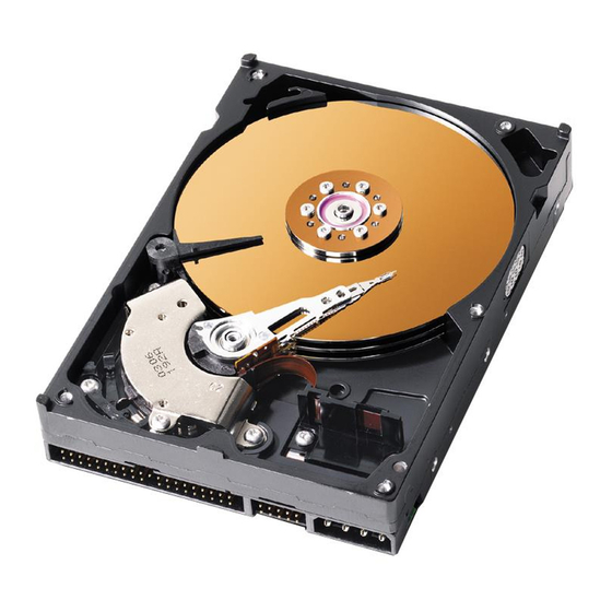
IBM storage products - official published specifications
Hard disk drive specifications
Deskstar 120 GXP
3.5 inch Ultra ATA/100 hard disk drive
Models:
IC35L020AVVN07
IC35L040AVVN07
IC35L060AVVA07
IC35L080AVVA07
IC35L100AVVA07
IC35L120AVVA07
Revision 4.1
S07N-4778-08
IBM
18 June 2002
Publication #2820
Advertisement
Table of Contents

Related Manuals for IBM IC35L040AVVN07-0 - 40GB IDE Deskstar 120GXP 7200RPM UATA-100 07N9682


Summary of Contents for IBM IC35L040AVVN07-0 - 40GB IDE Deskstar 120GXP 7200RPM UATA-100 07N9682
-
Page 1: Hard Disk Drive Specifications
IBM storage products - official published specifications Hard disk drive specifications Deskstar 120 GXP 3.5 inch Ultra ATA/100 hard disk drive Models: IC35L020AVVN07 IC35L040AVVN07 IC35L060AVVA07 IC35L080AVVA07 IC35L100AVVA07 IC35L120AVVA07 Revision 4.1 18 June 2002 S07N-4778-08 Publication #2820... - Page 2 This page intentionally left blank.
- Page 3 IBM storage products - official published specifications Hard disk drive specifications Deskstar 120 GXP 3.5 inch Ultra ATA/100 hard disk drive Models: IC35L020AVVN07 IC35L040AVVN07 IC35L060AVVA07 IC35L080AVVA07 IC35L100AVVA07 IC35L120AVVA07 Revision 4.1 18 June 2002 S07N-4778-08 Publication #2820...
- Page 4 IBM may have patents or pending patent applications covering subject matter in this document. The furnishing of this document does not give you any license to these patents. You can send license inquiries in writing to the IBM Director of Commercial Relations, IBM Corporation, Armonk, NY 10577.
-
Page 5: Table Of Contents
Table of contents List of figures ..............1.0 General . - Page 6 6.5 DC power requirements ............6.5.1 Input voltage .
- Page 7 8.11 Sector Count Register ............8.12 Sector Number Register .
- Page 8 11.0 Command descriptions ........... . 11.1 Check Power Mode (E5h/98h) .
- Page 9 11.36 Write Buffer (E8h) ............11.37 Write DMA (CAh/CBh) .
- Page 10 This page intentionally left blank.
-
Page 11: List Of Figures
List of figures Figure 1. Formatted capacity ............Figure 2. - Page 12 Figure 51. Temperature and humidity ..........Figure 52.
- Page 13 Figure 104. Identify Device Information (part 5 of 6) ........Figure 105.
- Page 14 Figure 158. Write Multiple Command (C5h) ......... . Figure 159.
-
Page 15: General
1.0 General This document describes the specifications of the Deskstar 120GXP, an IBM 3.5-inch 7200-rpm ATA interface hard disk drive with the following model numbers: IC35L020AVVN07 (20 GB) IC35L040AVVN07 (40 GB) IC35L060AVVA07 (60 GB) IC35L080AVVA07 (80 GB) IC35L100AVVA07 (100 GB) - Page 16 This page intentionally left blank.
-
Page 17: General Features
2.0 General features ! Data capacities of 20 GB - 120 GB ! Spindle speeds of 7200 RPM ! Enhanced IDE interface ! Sector format of 512 bytes/sector ! Closed-loop actuator servo ! Load/Unload mechanism, non head disk contact start/stop ! Automatic Actuator lock ! Interleave factor 1:1 ! Seek time of 8.5 ms in Read Operation (8.2 ms typical without Command Overhead) (2 and 3... - Page 18 This page intentionally left blank.
-
Page 19: Part 1. Functional Specification
Part 1. Functional specification Deskstar 120GXP hard disk drive specifications... - Page 20 This page intentionally left blank.
-
Page 21: Fixed Disk Subsystem Description
3.0 Fixed disk subsystem description 3.1 Control Electronics The drive is electronically controlled by a microprocessor, several logic modules, digital/analog modules, and various drivers and receivers. The control electronics performs the following major functions: ! Controls and interprets all interface signals between the host controller and the drive. ! Controls read write accessing of the disk media, including defect management and error recovery. - Page 22 This page intentionally left blank.
-
Page 23: Drive Characteristics
4.0 Drive characteristics This section describes the characteristics of the drive. 4.1 Default logical drive parameters The default of the logical drive parameters in Identify Device data is as shown below. Description IC35L020AVVN07 IC35L040AVVN07 IC35L060AVVA07 Physical Layout Label capacity (GB) 20.5 41.1 61.4... -
Page 24: Data Sheet
Logical layout: Logical layout is an imaginary drive parameter (that is, the number of heads) which is used to access the drive from the system interface. The Logical layout to Physical layout (that is, the actu- al Head and Sectors) translation is done automatically in the drive. The default setting can be obtained by issuing an IDENTIFY DEVICE command 4.2 Data sheet Description... -
Page 25: Drive Organization
4.3 Drive organization 4.3.1 Drive format Upon shipment from IBM manufacturing the drive satisfies the sector continuity in the physical format by means of the defect flagging strategy described in Section 5.0 on page 19 in order to provide the maximum performance to users. - Page 26 This cylinder contains the user data which can be sent and retrieved via read/write commands and a spare area for reassigned data. Spare cylinder The spare cylinder is used by IBM manufacturing and includes data sent from a defect location. Deskstar 120GXP hard disk drive specifications...
-
Page 27: Performance Characteristics
4.4 Performance characteristics Drive performance is characterized by the following parameters: ! Command overhead ! Mechanical positioning - Seek time - Latency ! Data transfer speed ! Buffering operation (Look ahead/Write cache) All the above parameters contribute to drive performance. There are other parameters that contribute to the performance of the actual system. -
Page 28: Figure 6. Full Stroke Seek Time
The terms “Typical” and “Max” are used throughout this specification with the following meanings: Typical. The average of the drive population tested at nominal environmental and voltage con- ditions. Max. The maximum value measured on any one drive over the full range of the environmental and voltage conditions. -
Page 29: Drive Ready Time
4.4.2.4 Cylinder switch time (Cylinder skew) Cylinder switch time - typical (ms) 56.7 kTPI 54 kTPI Figure 8. Cylinder switch time Cylinder switch time is defined as the amount of time required by the fixed disk to access the next sequential block after reading the last sector in the current cylinder. -
Page 30: Data Transfer Speed
4.4.4 Data transfer speed 120 GB model Data transfer speed (Mbyte/sec) Disk-Buffer transfer (Zone 0) Instantaneous - typical 57.2 Sustained - read typical 48.0 Disk-Buffer transfer (Zone 30) Instantaneous - typical 27.6 Sustained - read typical 23.2 Buffer-Host (max) Figure 12. Data transfer speed ! Instantaneous disk-buffer transfer rate (Mbyte/sec) is derived by the following formula: 512 (Number of sectors on a track) (revolution per second) Note: The number of sectors per track will vary because of the linear density recording. -
Page 31: Throughput
4.4.5 Throughput 4.4.5.1 Simple sequential access The following figure illustrates the case of the three-disk enclosure. Operation Typical (sec) Max (sec) Sequential Read (Zone 0) 0.38 0.40 Sequential Read (Zone 30) 0.77 0.81 Figure 13. Simple Sequential Access performance The above table gives the time required to read a total of 8000h consecutive blocks (16,777,216 bytes) accessed by 128 read commands. -
Page 32: Operating Modes
4.4.6 Operating modes 4.4.6.1 Operating mode descriptions Operating mode Description Spin-up Start up time period from spindle stop or power down Seek Seek operation mode Write Write operation mode Read Read operation mode Unload Idle Spindle rotation at 7200 RPM with heads unloaded Idle Spindle motor and servo system are working normally. -
Page 33: Defect Flagging Strategy
5.0 Defect flagging strategy Media defects are remapped to the next available sector during the Format Process in manufacturing. The mapping from LBA to the physical locations is calculated by an internally maintained table. Shipped format ! Data areas are optimally used. ! No extra sector is wasted as a spare throughout user data areas. - Page 34 This page intentionally left blank.
-
Page 35: Specification
6.0 Specification Electrical interface 6.1.1 Connector location Refer to the following illustration to see the location of the connectors. Figure 17. Connector location (2 and 3 disk model shown) 6.1.1.1 DC power connector The DC power connector is designed to mate with AMP part number 1-480424-0 using AMP pins part number 350078-4 (strip), part number 61173-4 (loose piece), or their equivalents. -
Page 36: Signal Definition
6.1.2 Signal definition The pin assignments of interface signals are listed in the figure below: SIGNAL Type SIGNAL Type RESET- 3-state 3-state 3-state 3-state 3-state DD10 3-state 3-state DD11 3-state 3-state DD12 3-state 3-state DD13 3-state 3-state DD14 3-state 3-state DD15 3-state (20) - Page 37 DD0-DD15 16-bit bi-directional data bus between the host and the drive. The lower 8 lines, DD00-07, are used for Register and ECC access. All 16 lines, DD00-15, are used for data transfer. These are 3-State lines with 24 mA current sink capability. DA0-DA2 Address used to select the individual register in the drive.
- Page 38 If device 1 did not assert DASP- during reset initialization, device 0 shall post its own status immediately after it completes diagnostics and clear the device 1 Status register to 00h. Device 0 may be unable to accept commands until it has finished its reset procedure and is ready (DRDY=1).
-
Page 39: Interface Logic Signal Levels
DDMARDY- (Ultra DMA) This signal is used only for Ultra DMA data transfers between the host and the device. DDMARDY- is a flow control signal for Ultra DMA data out bursts. This signal is held asserted by the device to indicate to the host that the device is ready to receive Ultra DMA data out transfers. -
Page 40: Signal Timings
6.2 Signal timings 6.2.1 Reset timings Drive reset timing. RESET- BUSY Figure 21. System reset timing chart PARAMETER DESCRIPTION Min (sec) Max (sec) RESET low width RESET high to not BUSY – Figure 22. System reset timing Deskstar 120GXP hard disk drive specifications... -
Page 41: Pio Timings
6.2.2 PIO timings The PIO cycle timings meet Mode 4 of the ATA/ATAPI-6 description. CS(1:0) DA(2:0) DIOR-, DIOW- Write data DD(15:0) Read data DD(15:0) t7(*) t8(*) IOCS16-(*) IORDY (*) Up to ATA-2 (mode-0,1,2) Figure 23. PIO cycle timings chart PARAMETER DESCRIPTION MIN (ns) MAX (ns) Cycle time... -
Page 42: Write Drq Interval Time
6.2.2.1 Write DRQ interval time For write sectors and write multiple operations 3.8 s is inserted from the end of negation of the DRQ bit until setting of the next DRQ bit. 6.2.2.2 Read DRQ interval time For read sectors and read multiple operations the interval from the end of negation of the DRQ bit until setting of the next DRQ bit is as follows: ! In the event that a host reads the status register only before the sector or block transfer DRQ interval, the DRQ interval 4.2 s... -
Page 43: Multiword Dma Timings
6.2.3 Multiword DMA timings The Multiword DMA timing meets Mode 2 of the ATA/ATAPI-6 description. CS0-/CS1- tLR/tLW DMARQ DMACK- tKR/tKW DIOR-/DIOW- READ DATA WRITE DATA Figure 25. Multiword DMA cycle timing chart PARAMETER DESCRIPTION MIN (ns) MAX (ns) Cycle time –... -
Page 44: Ultra Dma Timings
6.2.4 Ultra DMA timings The Ultra DMA timing meets Mode 0,1,2,3 4, and 5 of the Ultra DMA Protocol. 6.2.4.1 Initiating Read DMA DMARQ DMACK- tENV tACK STOP tENV tACK t2CYC HDMARDY- tCYC tCYC tZIORDY tDZFS DSTROBE tZAD DD(15:00) xxxxxxxxxxxxxxxxxxxxxxxxx RD Data RD Data RD Data... -
Page 45: Figure 29. Ultra Dma Cycle Timing Chart (Host Pausing Read)
6.2.4.2 Host Pausing Read DMA DMARQ DMACK- STOP HDMARDY- tRFS DSTROBE Figure 29. Ultra DMA cycle timing chart (Host pausing Read) MODE0 MODE1 MODE2 MODE3 MODE4 MODE5 PARAMETER DESCRIPTION (all values in ns) DSTROBE to HDMARDY– time – – – –... -
Page 46: Figure 31. Ultra Dma Cycle Timing Chart (Host Terminating Read)
6.2.4.3 Host Terminating Read DMA DMARQ tMLI DMACK- tACK STOP tACK HDMARDY- tRFS tIORDYZ DSTROBE DD(15:00) xxx RD Data xxxxxxxxxxxxxxxxxx xxxxxxxxxx tZAH Device drives DD Host drives DD Figure 31. Ultra DMA cycle timing chart (Host terminating Read) MODE0 MODE1 MODE2 MODE3 MODE4... -
Page 47: Figure 33. Ultra Dma Cycle Timing Chart (Device Terminating Read)
6.2.4.4 Device Terminating Read DMA DMARQ tMLI DMACK- tACK STOP tACK HDMARDY- tIORDYZ DSTROBE DD(15:00) xxxxx xxxxxxxxxxxxxxxxxx xxxxxxxxxx tZAH Host drives DD Device drives DD Figure 33. Ultra DMA cycle timing chart (Device terminating Read) MODE0 MODE1 MODE2 MODE3 MODE4 MODE5 PARAMETER DESCRIPTION (all values in ns) -
Page 48: Figure 35. Ultra Dma Cycle Timing Chart (Initiating Write)
6.2.4.5 Initiating Write DMA DMARQ DMACK- tACK tENV STOP tZIORDY t2CYC DDMARDY- tACK tCYC tCYC HSTROBE DD(15:0) xxxxxxxxxxxxxxxxxxxxxxxxxxxxxxx WT Data WT Data WT Data Host drives DD Figure 35. Ultra DMA cycle timing chart (Initiating Write) MODE0 MODE1 MODE2 MODE3 MODE4 MODE5 PARAMETER DESCRIPTION... -
Page 49: Figure 37. Ultra Dma Cycle Timing Chart (Device Pausing Write)
6.2.4.6 Device Pausing Write DMA DMARQ DMACK- STOP DDMARDY- tRFS HSTROBE Figure 37. Ultra DMA cycle timing chart (Device Pausing Write) MODE0 MODE1 MODE2 MODE3 MODE4 MODE5 PARAMETER DESCRIPTION (all values in ns) HSTROBE to DDMARDY– – – – – –... -
Page 50: Figure 39. Ultra Dma Cycle Timing Chart (Device Terminating Write)
6.2.4.7 Device Terminating Write DMA DMARQ tMLI DMACK- tACK STOP tIORDYZ DDMARDY- tACK tRFS HSTROBE DD(15:00) xxxxxxxxxxxxxxxxxxxxxxxxxx xxxxxxxxxx xxx WT Data Host drives DD Figure 39. Ultra DMA cycle timing chart (Device Terminating Write) MODE0 MODE1 MODE2 MODE3 MODE4 MODE5 PARAMETER DESCRIPTION (all values in ns) DDMARDY to final HSTROBE... -
Page 51: Figure 41. Ultra Dma Cycle Timing Chart (Host Terminating Write)
6.2.4.8 Host Terminating Write DMA DMARQ tMLI DMACK- tACK STOP tIORDYZ DDMARDY- tACK HSTROBE DD(15:00) xxxxxxxxxxxxxxxxxxxxxxxxxxxxxxxxxxxxx xxxxxxxxxx Host drives DD Figure 41. Ultra DMA cycle timing chart (Host Terminating Write) MODE0 MODE1 MODE2 MODE3 MODE4 MODE5 PARAMETER DESCRIPTION (all values in ns) Time from HSTROBE to edge –... -
Page 52: Addressing Of Registers
6.2.5 Addressing of registers The host addresses the drive through a set of registers called the Task File. These registers are mapped into the I/ O space of the host. Two chip select lines (CS0– and CS1–) and three address lines (DA0-02) are used to select one of these registers, while a DIOR–... -
Page 53: Jumper Settings
6.3 Jumper settings 6.3.1 Jumper pin location Jumper pins Figure 44. Jumper pin location (2 and 3 disk model shown) 6.3.2 Jumper pin identification Pin I Pin A DERA001.prz Pin B Figure 45. Jumper pin identification (2 and 3 disk model shown) Deskstar 120GXP hard disk drive specifications... -
Page 54: Jumper Pin Assignment
6.3.3 Jumper pin assignment There are four jumper settings as shown in the following sections: 16 logical head default (normal use) 15 logical head default 2 GB/32 GB clip Power up in standby Within each of these four jumper settings the pin assignment selects Device 0, Device 1, Cable Selection, or Device 1 Slave Present as shown in the following figures. -
Page 55: Jumper Positions
6.3.4 Jumper positions 6.3.4.1 16 logical head default (normal use) The figure below shows the jumper positions used to select Device 0, Device 1, Cable Selection, or Device 1 (Slave) Present. DEVICE 0 (Master) DEVICE 1 (Slave) CABLE SEL DEVICE 1 (Slave) Present Shipping Default Condition (DEVICE 0) -
Page 56: Figure 48. Jumper Positions For 15 Logical Head Default
6.3.4.2 15 logical head default The figure below shows the jumper positions used to select Device 0, Device 1, Cable Selection, or Device 1 (Slave) Present setting 15 logical heads instead of default 16 logical head models. DEVICE 0 (Master) DEVICE 1 (Slave) CABLE SEL DEVICE 1 (Slave) Present... -
Page 57: Figure 49. Jumper Positions For Capacity Clip To 2Gb/32Gb
6.3.4.3 Capacity clip to 2GB/32GB The figure below shows the jumper positions used to select Device 0, Device 1, Cable Selection, or Device 1 (Slave) Present while setting the drive capacity down either to 2GB or 32GB for the purpose of compatibility. -
Page 58: Figure 50. Jumper Settings For Disabling Auto Spin
6.3.4.4 Power Up In Standby The figure below shows the jumper positions used to select Device 0, Device 1, Cable Selection, or Device 1 (Slave) Present to enable Power Up In Standby. DEVICE 0 (Master) DEVICE 1 (Slave) CABLE SEL DEVICE 1 (Slave) Present Figure 50. -
Page 59: Environment
6.4 Environment 6.4.1 Temperature and humidity Operating conditions Temperature 5 to 55°C Relative humidity 8 to 90% non-condensing Maximum wet bulb temperature 29.4°C non-condensing Maximum temperature gradient 15°C/Hour Altitude –300 to 3,048 m Non operating conditions Temperature –40 to 65°C Relative humidity 5 to 95% non-condensing Maximum wet bulb temperature... -
Page 60: Corrosion Test
Environment Specification 36C/95% 31C/90% Wet Bulb 35C Wet Bulb 29.4C Nonoperating Operating 65C/14% 55C/15% Temperature (C) Figure 52. Limits of temperature and humidity Note: Storage temperature range is 0° to 65°. 6.4.2 Corrosion test The drive shows no sign of corrosion inside and outside of the hard disk assembly and is functional after being subjected to seven days at 50°C with 90% relative humidity. -
Page 61: Dc Power Requirements
6.5 DC power requirements The following voltage specifications apply at the power connector of the drive. Damage to the drive electronics may result if the power supply cable is connected or disconnected while power is being applied to the drive (no hot plug/unplug is allowed). Connections to the drive should be made in a low voltage, iso- lated secondary circuit (SELV). -
Page 62: Figure 55. Power Supply Current Of 80 Gb And 60 Gb Models
Power supply current of 80 GB +5 Volts [mA] +12 Volts [mA] Total and 60 GB models (values in milliamps. RMS) Pop Mean Std Dev Pop Mean Std Dev Idle average Idle ripple (peak-to-peak) Low RPM Idle Low RPM Idle Ripple Unload Idle average Unload Idle Ripple Seek average... -
Page 63: Power Supply Generated Ripple At Drive Power Connector
6.5.3 Power supply generated ripple at drive power connector Maximum (mV pp) +5V DC 0-10 +12V DC 0-10 Figure 57. Power supply generated ripple at drive power connector During drive start up and seeking 12-volt ripple is generated by the drive (referred to as dynamic loading). If the power of several drives is daisy chained together, the power supply ripple plus the dynamic loading of the other drives must remain within the above regulation tolerance. -
Page 64: Reliability
6.6 Reliability 6.6.1 Data integrity No more than one sector is lost at Power loss condition during the write operation when the write cache option is disabled. If the write cache option is active, the data in write cache will be lost. To prevent the loss of customer data, it is recommended that the last write access before power off be issued after setting the write cache off. -
Page 65: Mechanical Specifications
6.7 Mechanical specifications 6.7.1 Physical dimensions 25.4 ± 0.4 101.6 ± 0.4 146 ± 0.6 BREATHER HOLE (*) Dia. 2.0 ± 0.1 38.9 ± 0.4 19.7 ± 0.4 LEFT FRONT * DO NOT BLOCK THE BREATHER HOLE. Figure 58. Top and side views of 60 GB - 120 GB models with mechanical dimensions All dimensions are in millimeters. -
Page 66: Figure 59. Bottom And Side Views Of 20Gb And 40Gb Models With Breather Hole And
BREATHER HOLE Figure 59. Bottom and side views of 20GB and 40GB models with breather hole and mounting hole locations All dimensions in the above figure are in millimeters. The breather hole must be kept uncovered in order to keep the air pressure inside of the disk enclosure equal to external air pressure. -
Page 67: Hole Locations
6.7.2 Hole locations The mounting hole location and size for the hard disk drive is shown below. (6X) Max. penetration 4.5 mm Side View I/F Connector Bottom View (4X) Max. penetration 4.0 mm Thread 6-32 UNC 41.28±0.5 44.45±0.2 95.25±0.2 6.35±0.2 28.5±0.5 60.0±0.2 41.6±0.2... -
Page 68: Connector Locations
6.7.3 Connector locations Figure 62. Connector locations 6.7.4 Drive mounting The drive will operate in all axes (6 directions). Performance and error rate will stay within specification limits if the drive is operated in the other orientations from which it was formatted. For reliable operation, the drive must be mounted in the system securely enough to prevent excessive motion or vibration of the drive during seek operation or spindle rotation, using appropriate screws or equivalent mounting hardware. -
Page 69: Vibration And Shock
6.8.1 Operating vibration 6.8.1.1 Random vibration The hard disk drive meets IBM Standard C-S 1-9711-002 (1990-03) for the V5L applied to horizontal direction and V4 applied to vertical direction. The test is 30 minutes of random vibration using the power spectral density (PSD) levels shown below in each of three mutually perpendicular axes. -
Page 70: Operating Shock
! 3 minutes dwell at two major resonances 6.8.3 Operating shock The drive meets IBM Standard C-S 1-9711-007 for the S5 product classification. The drive meets the following criteria while operating in the conditions described below. The shock test consists of 10 shock inputs in each axis and direction for total of 60. -
Page 71: Rotational Shock
6.8.4.2 Sinusoidal shock wave The shape is approximately half-sine pulse. The figure below shows the maximum acceleration level and duration. Models Accleration level (G) Duration (ms) 1 and 3 disk models 2 disk models All models Figure 65. Sinusoidal shock wave 6.8.5 Rotational shock All shock inputs shall be applied around the actuator pivot axis. -
Page 72: Acoustics
6.9 Acoustics The upper limit criteria of the octave sound power levels are given in Bels relative to one picowatt and are shown in the following table. The sound power emission levels are measured in accordance with ISO 7779. Typical Mode 1 and 3 disk 2 disk models... -
Page 73: Identification Labels
The following labels are affixed to every drive shipped from the drive manufacturing location in accordance with the appropriate hard disk drive assembly drawing: • A label containing the IBM logo, the IBM part number, and the statement “Made by IBM Japan Ltd.” or IBM approved equivalent •... -
Page 74: Safety
Halon 1301 and Halon 2402. Although not specified by the Protocol, CFC-112 is also controlled. In addition to the Protocol IBM requires the following: ! that no packaging used for the shipment of the product use controlled CFCs in the manufacturing process. -
Page 75: Electromagnetic Compatibility
EMC requirements: ! United States Federal Communications Commission (FCC) Rules and Regulations (Class B), Part 15. IBM Corporate Standard C-S 2-0001-026 (A 6 dB buffer shall be maintained on the emission requirements). ! European Economic Community (EEC) directive number 76/889 related to the control of radio fre- quency interference and the Verband Deutscher Elektrotechniker (VDE) requirements of Germany (GOP). - Page 76 This page intentionally left blank.
-
Page 77: Part 2. Interface Specification
Part 2. Interface specification Deskstar 120GXP hard disk drive specifications... - Page 78 This page intentionally left blank.
-
Page 79: General
7.0 General This specification describes the host interface of the Deskstar 120GXP hard disk drive. The interface conforms to the Working Document of Information Technology - AT Attachment with Packet Interface Extension (ATA/ATAPI-5), Revision 3, dated 29 February 2000, with certain limitations described in 7.2, “Deviations from standard.”... - Page 80 This page intentionally left blank.
-
Page 81: Registers
8.0 Registers Addresses Functions CS0– CS1– READ (DIOR–) WRITE (DIOW–) Data bus high impedance Not used Control block registers Data bus high impedance Not used Data bus high impedance Not used Alternate Status Device Control Device Address Not used Command block registers Data Data Error Register... -
Page 82: Alternate Status Register
8.1 Alternate Status Register Alternate Status Register DSC/ SERV Figure 69. Alternate Status Register This register contains the same information as the Status Register. The only difference is that reading this register does not imply interrupt acknowledge or clear a pending interrupt. See 8.13, “Status Register” on page 72 for the definition of the bits in this register. -
Page 83: Data Register
8.5 Data Register This register is used to transfer data blocks between the device data buffer and the host. It is also the register through which sector information is transferred on a Format Track command and configuration information is transferred on an Identify Device command. All data transfers are 16 bits wide, except for ECC byte transfers which are 8 bits wide. -
Page 84: Device/Head Register
-DS1 -Drive Select 1. Drive select bit for device 1, active low. DS1=0 when device 1 (slave) is selected and active. -DS0 -Drive Select 0. Drive select bit for device 0, active low. DS0=0 when device 0 (master) is selected and active. 8.8 Device/Head Register Device/Head Register Figure 72. -
Page 85: Features Register
Bit Definitions ICRCE Interface CRC Error. CRC=1 indicates a CRC error has occurred on the data bus (CRC) during Ultra-DMA transfer. Uncorrectable Data Error. UNC=1 indicates an uncorrectable data error has been encountered. IDNF (IDN) ID Not Found. IDN=1 indicates the ID field of the requested sector could not be found. ABRT Aborted Command. -
Page 86: Status Register
8.13 Status Register Status Register DSC/ DRDY CORR SERV Figure 74. Status Register This register contains the device status. The contents of this register are updated whenever an error occurs and at the completion of each command. If the host reads this register when an interrupt is pending, it is considered to be the interrupt acknow- ledge. -
Page 87: General Operation
9.0 General operation 9.1 Reset response There are three types of resets in ATA: Power On Reset (POR). The device executes a series of electrical circuitry diagnostics, spins up the HDA, tests speed and other mechanical parameters, and sets default values. Hard Reset (Hardware Reset). -
Page 88: Register Initialization
9.2 Register initialization After power on, hard reset, or software reset, the register values are initialized as shown in the figure below. Register Default Value Error Diagnostic Code Sector Count Sector Number Cylinder Low Cylinder High Device/Head Status Alternate Status Figure 76. -
Page 89: Diagnostic And Reset Considerations
9.3 Diagnostic and reset considerations For each Reset and Execute Device Diagnostic the diagnostic is done as follows: Power On Reset. DASP- is read by Device 0 to determine if Device 1 is present. If Device 1 is present, Device 0 shall read PDIAG- to determine when it is valid to clear the BSY bit and whether Device 1 has powered on or reset without error. -
Page 90: Sector Addressing Mode
9.4 Sector Addressing Mode All addressing of data sectors recorded on the drive media is by a logical sector address. The logical CHS address for the drive is different from the actual physical CHS location of the data sector on the disk media. -
Page 91: Overlapped And Queued Feature
9.5 Overlapped and queued feature Overlap allows devices to perform a bus release so that the other device on the bus may be used. To perform a bus release the device clears both DRQ and BSY to zero. When selecting the other device during overlapped operations, the host shall disable interrupts via the nIEN bit on the currently selected device before writing the Device/Head register to select the other device. -
Page 92: Power Management Feature
9.6 Power management feature The power management feature functions permit a host to reduce the power required to operate the drive. It provides a set of commands and a timer that enables a device to implement low power consumption modes. The drive implements the following set of functions: ! Standby timer ! Idle command... -
Page 93: Interface Capability For Power Modes
9.6.4 Interface capability for power modes Each power mode affects the physical interface as defined in the following table. Interface Mode Media active Active Active Idle Active Standby Inactive Sleep Inactive Figure 79. Power conditions Ready (RDY) is not a power condition. A device may post ready at the interface even though the media may not be accessible. -
Page 94: Function
9.7 S.M.A.R.T. function The intent of Self-Monitoring Analysis and Reporting Technology (S.M.A.R.T) is to protect user data and prevent unscheduled system downtime that may be caused by predictable degradation and/or fault of the device. By monitoring and storing critical performance and calibration parameters, S.M.A.R.T devices employ sophisticated data analysis algorithms to predict the likelihood of near-term degradation or fault condition. -
Page 95: Self-Test
vendor specific information on these reported errors. The error log is not disabled when SMART is disabled. Disabling SMART disables the delivering of error log information via the SMART READ LOG SECTOR command. If a device receives a firmware modification, all error log data is discarded and the device error count for the life of the device is reset to zero. -
Page 96: Security Mode Feature Set
9.8 Security Mode Feature Set Security Mode Feature Set is a powerful security feature. With a device lock password, a user can prevent unauthorized access to a hard disk drive even if the device is removed from the computer. The following commands are supported for this feature: ('F1'h) Security Set Password ('F2'h) -
Page 97: Operation Example
The system manufacturer or dealer who intends to enable the device lock function for end-users must set the master password even if only single level password protection is required. 9.8.4 Operation example 9.8.4.1 Master Password setting The system manufacturer or dealer can set a new Master Password from default Master Password using the Security Set Password command without enabling the Device Lock Function. -
Page 98: Figure 81. Usual Operation
9.8.4.3 Operation from POR after User Password is set When Device Lock Function is enabled, the device rejects media access command until a Security Unlock command is successfully completed. Device Locked mode Unlock CMD Erase Prepare Media Access Non-media access Command (*1) Command (*1) Erase Unit... -
Page 99: Figure 82. Password Lost
9.8.4.4 User Password Lost If the User Password is forgotten and High level security is set, the system user cannot access any data. However the device can be unlocked using the Master Password. If a system user forgets the User Password and Maximum security level is set, data access is impossible. However the device can be unlocked using the Security Erase Unit command to unlock the device and erase all user data with the Master Password. -
Page 100: Command Table
9.8.5 Command table This table shows the response of the device to commands when the Security Mode Feature Set (Device lock function) is enabled. Command Locked Mode Unlocked Mode Frozen Mode Check Power Mode Executable Executable Executable Execute Device Diagnostic Executable Executable Executable... -
Page 101: Figure 84. Command Table For Device Lock Operation (Part 2 Of 2)
Command Locked Mode Unlocked Mode Frozen Mode SMART Enable Operations Executable Executable Executable SMART Execute Off-line Immediate Executable Executable Executable SMART Read Attribute Values Executable Executable Executable SMART Read Attribute Thresholds Executable Executable Executable SMART Return Status Executable Executable Executable SMART Save Attribute Values Executable Executable... -
Page 102: Host Protected Area Function
9.9 Host Protected Area Function The Host Protected Area Function provides a protected area which cannot be accessed via conventional methods. This protected area is used to contain critical system data such as BIOS or system management information. The contents of the main memory of the entire system may also be dumped into the protected area to resume after system power off. -
Page 103: Security Extensions
4. Advanced usage using protected area The data in the protected area is accessed by the following method: Issue Read Native Max Address command to get the real device maximum LBA. Returned value shows that native device maximum LBA is 12,692,735 (C1ACFFh) regardless of the current setting. -
Page 104: Seek Overlap
9.10 Seek Overlap The Travelstar 120GXP provides an accurate method for measuring seek time. The seek command is usually used to measure the device seek time by accumulating the execution time for a number of seek commands. With typical implementation of seek command this measurement must include the device and host command overhead. -
Page 105: Write Cache Function
9.11 Write cache function Write cache is a performance enhancement whereby the device reports the completion of the write com- mand (Write Sectors, Write Multiple, and Write DMA) to the host as soon as the device has received all of the data into its buffer. -
Page 106: Recovered Read Errors
9.13.3 Recovered read errors When a read operation for a sector has failed once and then has recovered at the specific ERP step, this sector of data is automatically reallocated. A media verification sequence may be run prior to the reallocation according to the predefined conditions. -
Page 107: Automatic Acoustic Management Feature Set (Aam)
9.16 Automatic Acoustic Management feature set (AAM) This feature set allows the host to select an acoustic management level. The acoustic management level may range from the lowest acoustic emanation setting of 01h to the maximum performance level of FEh. Device performance and acoustic emanation may increase with increasing acoustic management levels. -
Page 108: Identify Device Data
Disable Address Offset Feature removes the address offset and sets the size of the drive reported by the Identify Device command back to the size specified in the last nonvolatile Set Max Address command. Before Enable Address Offset Mode A reserved area has been created using a nonvolatile Set Max command. Non-Accessible Accessible (System reserved... -
Page 109: Command Protocol
10.0 Command Protocol The commands are grouped into different classes according to the protocols followed for command execution. The command classes with their associated protocols are defined below. For all commands, the host must first check if BSY=1, and should proceed no further unless and until BSY=0. -
Page 110: Pio Data In Commands
10.1 PIO Data In commands These commands are ! Device Configuration Identify ! Identify Device ! Read Buffer ! Read Long ! Read Multiple ! Read Sectors ! S.M.A.R.T. Read Attribute Values ! S.M.A.R.T. Read Attribute Thresholds ! S.M.A.R.T. Read Log Sector Execution includes the transfer of one or more 512 byte (>512 bytes on Read Long) sectors of data from the device to the host. - Page 111 If the device detects an invalid parameter, it will abort the command by setting BSY=0, ERR=1, ABT=1, and interrupting the host. If an error occurs, the device will set BSY=0, ERR=1, and DRQ=1. The device will then store the error status in the Error Register and interrupt the host.
-
Page 112: Pio Data Out Commands
10.2 PIO Data Out commands These commands are PIO Data Out commands: ! Device Configuration Set ! Format Track ! Security Disable Password ! Security Erase Unit ! Security Set Password ! Security Unlock ! Set Max Set Password command ! Set Max Unlock command ! SMART Write Log Sector ! Write Buffer... - Page 113 The Write Multiple command transfers one block of data for each interrupt. The other commands transfer one sector of data for each interrupt. If the device detects an invalid parameter, it will abort the command by setting BSY=0, ERR=1, ABT=1, and interrupting the host.
-
Page 114: Non-Data Commands
10.3 Non-data commands The following are non-data commands: ! Check Power Mode ! Device Configuration Freeze Lock ! Device Configuration Restore ! Execute Device Diagnostic ! Flush Cache ! Idle ! Idle Immediate ! Initialize Device Parameters ! NOP ! Read Native Max Address ! Read Verify Sectors ! Recalibrate ! Security Erase Prepare... -
Page 115: Dma Commands
10.4 DMA commands DMA commands are ! Read DMA ! Write DMA Data transfers using DMA commands differ in two ways from PIO transfers: ! data transfers are performed using the slave DMA channel ! no intermediate sector interrupts are issued on multisector commands Initiation of the DMA transfer commands is identical to the Read Sector or Write Sector commands except that the host initializes the slave-DMA channel prior to issuing the command. -
Page 116: Dma Queued Commands
10.5 DMA queued commands DMA queued commands are ! Read DMA Queued ! Service ! Write DMA Queued 1. Command Issue a. The host writes any required parameters to the Features, Sector Count, Sector Number, Cylinder, and Device/Head registers. b. The host writes command code to the Command Register. c. -
Page 117: Command Descriptions
11.0 Command descriptions Pro- Code Binary Code Bit Command tocol (Hex) 7 6 5 4 3 2 1 0 Check Power Mode 1 1 1 0 0 1 0 1 Check Power Mode* 1 0 0 1 1 0 0 0 Device Configuration Restore 1 0 0 1 1 0 0 1 Device Configuration Freeze Lock... -
Page 118: Figure 88. Command Set (2 Of 2)
Pro- Code Binary Code Bit Command tocol (Hex) 7 6 5 4 3 2 1 0 Sleep 1 1 1 0 0 1 1 0 Sleep* 1 0 0 1 1 0 0 1 SMART Disable Operations 1 0 1 1 0 0 0 0 SMART Enable/Disable Attribute Autosave 1 0 1 1 0 0 0 0 SMART Enable Operations... -
Page 119: Figure 89. Command Set (Subcommands)
Command code Feature Command (Subcommand) (Hex) Register (Hex) (S.M.A.R.T Function) SMART Read Attribute Values SMART Read Attribute Thresholds SMART Enable/Disable Attribute Autosave SMART Save Attribute Values SMART Execute Off-line Data Collection SMART Read Log SMART Write Log SMART Enable Operations SMART Disable Operations SMART Return Status SMART Enable/Disable Automatic Off-line... - Page 120 LBA mode. Indicates the addressing mode. Zero specifies CHS mode and one specifies LBA addressing mode. Retry. Original meaning is obsoleted, there is no difference between 0 and 1. (Use of 0 is recommended for future compatibility.). Option Bit. Indicates that the Option Bit of the Sector Count Register should be specified. (This bit is used by Set Max Address command) Valid.
-
Page 121: Check Power Mode (E5H/98H)
11.1 Check Power Mode (E5h/98h) Command Block Output Command Block Input Registers Registers Register Register 7 6 5 4 3 2 1 0 7 6 5 4 3 2 1 0 Data - - - - - - - - Data - - - - - - - - Feature... -
Page 122: Device Configuration Overlay (B1H)
11.2 Device Configuration Overlay (B1h) Command Block Output Command Block Input Registers Registers Register Register 7 6 5 4 3 2 1 0 7 6 5 4 3 2 1 0 Data - - - - - - - - Data - - - - - - - - Feature... -
Page 123: Device Configuration Freeze Lock (Subcommand C1H)
11.2.2 DEVICE CONFIGURATION FREEZE LOCK (subcommand C1h) The DEVICE CONFIGURATION FREEZE LOCK command prevents accidental modification of the Device Configuration Overlay settings. After successful execution of a DEVICE CONFIGURATION FREEZE LOCK command, all DEVICE CONFIGURATION SET, DEVICE CONFIGURATION FREEZE LOCK, DEVICE CONFIGURATION IDENTIFY, and DEVICE CONFIGURATION RESTORE commands are aborted by the device. -
Page 124: Figure 93. Device Configuration Overlay Data Structure
Word Content 0001h Data Structure revision Multiword DMA modes supported 15-3 Reserved 1 = Multiword DMA mode 2 and below are supported 1 = Multiword DMA mode 1 and below are supported 1 = Multiword DMA mode 0 is supported Ultra DMA modes supported 15-6 Reserved... -
Page 125: Execute Device Diagnostic (90H)
11.3 Execute Device Diagnostic (90h) Command Block Output Command Block Input Registers Registers Register Register 7 6 5 4 3 2 1 0 7 6 5 4 3 2 1 0 Data - - - - - - - - Data - - - - - - - - Feature... -
Page 126: Flush Cache (E7H)
11.4 Flush Cache (E7h) Command Block Output Command Block Input Registers Registers Register 7 6 5 4 3 2 1 0 Register 7 6 5 4 3 2 1 0 Data Data - - - - - - - - - - - - - - - - Feature - - - - - - - -... -
Page 127: Format Track (50H)
11.5 Format Track (50h) Command Block Output Command Block Input Registers Registers Register 7 6 5 4 3 2 1 0 Register 7 6 5 4 3 2 1 0 Data - - - - - - - - Data - - - - - - - - Feature Error... - Page 128 Input parameters from the device Sector Number In LBA mode this register specifies current LBA address bits 0-7. (L=1) Cylinder High/Low In LBA mode this register specifies current LBA address bits 8-15 (Low), 16-23 (High). In LBA mode this register specifies current LBA address bits 24-27. (L=1) Error The Error Register.
-
Page 129: Format Unit (F7H)
11.6 Format Unit (F7h) Command Block Output Command Block Input Registers Registers Register 7 6 5 4 3 2 1 0 Register 7 6 5 4 3 2 1 0 Data Data - - - - - - - - - - - - - - - - Feature 0 0 0 1 0 0 0 1... -
Page 130: Identify Device (Ech)
11.7 Identify Device (ECh) Command Block Output Command Block Input Registers Registers Register Register 7 6 5 4 3 2 1 0 7 6 5 4 3 2 1 0 Data - - - - - - - - Data - - - - - - - - Feature - - - - - - - -... -
Page 131: Figure 100. Identify Device Information (Part 1 Of 6)
The Identify Device command requests the device to transfer configuration information to the host. The device will transfer a sector to the host containing the information described in the figure below. Note: * in the Content field indicates vendor specific use of those parameters. Word Content Description... -
Page 132: Figure 101. Identify Device Information (Part 2 Of 6)
Word Content Description 4000H Capabilities, bit assignments: 15-14(=01) Word 50 is valid 13– 1(=0) Reserved Minimum value of Standby timer (=0) less than 5 minutes (=1) equal to or greater than 5 minutes 0200H PIO data transfer cycle timing mode 0200H DMA data transfer cycle timing mode. -
Page 133: Figure 102. Identify Device Information (Part 3 Of 6)
Word Content Description 00XXH Queue depth 15- 5 Reserved 4- 0 Maximum queue depth 76-79 0000H Reserved 003CH Major version number 15- 0 (=3C)ATA-2, ATA-3, ATA/ATAPI-4, ATA/ATAPI-5 0015H Minor version number 15- 0 (=15)ATA/ATAPI-5 X3T13 1321D 74EBH Command set supported 15(=0) Reserved 14(=1) -
Page 134: Figure 103. Identify Device Information (Part 4 Of 6)
Word Content Description XXXXH Command set/feature enabled Reserved NOP command READ BUFFER command WRITE BUFFER command Reserved Host Protected Area feature set DEVICE RESET command SERVICE interrupt RELEASE interrupt LOOK AHEAD WRITE CACHE PACKET Command feature set Power management feature set Removable feature set Security feature set SMART feature set... -
Page 135: Figure 104. Identify Device Information (Part 5 Of 6)
Word Content Description XXXXH Time required for Security Erase Unit completion Time = value x 2 (minutes) 0000H Time required for Enhanced Security Erase completion 0000H Current advanced power management value FFFEH Master Password Revision Code XXXXH Hardware reset result. Bit assignments 15-14 (=01) Word 93 is valid CBLID- status... -
Page 136: Figure 105. Identify Device Information (Part 6 Of 6)
Word Content Description XXXXH Current Set Feature Option. Bit assignments 15- 4 Reserve Auto reassign 1= Enable Reverting 1= Enable Read Look-ahead 1= Enable Write Cache 1= Enable 130-159 XXXXH Reserved 160-254 0000H Reserved XXA5H 15- 8 Checksum. This value is the two's complement of the sum of all bytes in byte 0 through 510 7- 0 (A5) Signature Figure 105. -
Page 137: Idle (E3H/97H)
11.8 Idle (E3h/97h) Command Block Output Command Block Input Registers Registers Register Register 7 6 5 4 3 2 1 0 7 6 5 4 3 2 1 0 Data - - - - - - - - Data - - - - - - - - Feature - - - - - - - - Error... -
Page 138: Idle Immediate (E1H/95H)
11.9 Idle Immediate (E1h/95h) Command Block Output Command Block Input Registers Registers Register Register 7 6 5 4 3 2 1 0 7 6 5 4 3 2 1 0 Data - - - - - - - - Data - - - - - - - - Feature - - - - - - - -... -
Page 139: Initialize Device Parameters (91H)
11.10 Initialize Device Parameters (91h) Command Block Output Command Block Input Registers Registers Register Register 7 6 5 4 3 2 1 0 7 6 5 4 3 2 1 0 Data - - - - - - - - Data - - - - - - - - Feature... -
Page 140: Nop (00H)
11.11 NOP (00h) Command Block Output Command Block Input Registers Registers Register Register 7 6 5 4 3 2 1 0 7 6 5 4 3 2 1 0 Data - - - - - - - - Data - - - - - - - - Feature V V V V V V V V Error... -
Page 141: Read Buffer (E4H)
11.12 Read Buffer (E4h) Command Block Output Command Block Input Registers Registers Register Register 7 6 5 4 3 2 1 0 7 6 5 4 3 2 1 0 Data Data - - - - - - - - - - - - - - - - Feature - - - - - - - -... -
Page 142: Read Dma (C8H/C9H)
11.13 Read DMA (C8h/C9h) Command Block Output Command Block Input Registers Registers Register Register 7 6 5 4 3 2 1 0 7 6 5 4 3 2 1 0 Data Data - - - - - - - - - - - - - - - - Feature - - - - - - - -... - Page 143 The retry bit. This bit is ignored. Input parameters from the device Sector Count The number of requested sectors not transferred. This will be zero unless an unrecoverable error occurs. Sector Number The sector number of the last transferred sector. (L=0) In LBA mode this register contains current LBA bits 0 - 7.
-
Page 144: Read Dma Queued (C7H)
11.14 Read DMA Queued (C7h) Command Block Output Command Block Input Registers Registers Register Register 7 6 5 4 3 2 1 0 7 6 5 4 3 2 1 0 Data - - - - - - - - Data - - - - - - - - Feature... - Page 145 Input parameters from the device on bus release Sector Count Bits 7 - 3 (Tag) contain the Tag of the command being bus released. Bit 2 (REL) is set to one. Bit 1 (I/O) is cleared to zero. Bit 0 (C/D) is cleared to zero. Sector Number, Cylinder High/low, H n/a.
-
Page 146: Read Long (22H/23H)
11.15 Read Long (22h/23h) Command Block Output Command Block Input Registers Registers Register Register 7 6 5 4 3 2 1 0 7 6 5 4 3 2 1 0 Data - - - - - - - - Data - - - - - - - - Feature - - - - - - - -... - Page 147 Input parameters from the device Sector Count The number of requested sectors not transferred. Sector Number The sector number of the transferred sector. (L=0) In LBA mode this register contains current LBA bits 0 - 7. (L=1) Cylinder High/Low The cylinder number of the transferred sector. (L=0) In LBA mode this register contains current LBA bits 8 - 15 (Low), 16 - 23 (High).
-
Page 148: Read Multiple (C4H)
11.16 Read Multiple (C4h) Command Block Output Command Block Input Registers Registers Register Register 7 6 5 4 3 2 1 0 7 6 5 4 3 2 1 0 Data - - - - - - - - Data - - - - - - - - Feature - - - - - - - -... - Page 149 Sector Number The sector number of the last transferred sector. (L=0) In LBA mode this register contains current LBA bits 0 - 7. (L=1) Cylinder High/Low The cylinder number of the last transferred sector. (L=0) In LBA mode this register contains current LBA bits 8 - 15 (Low), 16 - 23 (High). (L=1) The head number of the last transferred sector.
-
Page 150: Read Native Max Address (F8H)
11.17 Read Native Max Address (F8h) Command Block Output Command Block Input Registers Registers Register Register 7 6 5 4 3 2 1 0 7 6 5 4 3 2 1 0 Data - - - - - - - - Data - - - - - - - - Feature... -
Page 151: Read Sectors (20H/21H)
11.18 Read Sectors (20h/21h) Command Block Output Command Block Input Registers Registers Register Register 7 6 5 4 3 2 1 0 7 6 5 4 3 2 1 0 Data - - - - - - - - Data - - - - - - - - Feature - - - - - - - -... - Page 152 Input parameters from the device Sector Count The number of requested sectors not transferred. This will be zero unless an unrecoverable error occurs. Sector Number The sector number of the last transferred sector. (L=0) In LBA mode this register contains current LBA bits 0 - 7. (L=1) Cylinder High/Low The cylinder number of the last transferred sector.
-
Page 153: Read Verify Sectors (40H/41H)
11.19 Read Verify Sectors (40h/41h) Command Block Output Command Block Input Registers Registers Register Register 7 6 5 4 3 2 1 0 7 6 5 4 3 2 1 0 Data - - - - - - - - Data - - - - - - - - Feature... - Page 154 Input parameters from the device Sector Count The number of requested sectors not verified. This will be zero unless an unrecoverable error occurs. Sector Number The sector number of the last transferred sector. (L=0) In LBA mode this register contains current LBA bits 0 - 7. (L=1) Cylinder High/Low The cylinder number of the last transferred sector.
-
Page 155: Recalibrate (1Xh)
11.20 Recalibrate (1xh) Command Block Output Command Block Input Registers Registers Register Register 7 6 5 4 3 2 1 0 7 6 5 4 3 2 1 0 Data - - - - - - - - Data - - - - - - - - Feature - - - - - - - - Error... -
Page 156: Security Disable Password (F6H)
11.21 Security Disable Password (F6h) Command Block Output Command Block Input Registers Registers Register Register 7 6 5 4 3 2 1 0 7 6 5 4 3 2 1 0 Data - - - - - - - - Data - - - - - - - - Feature... -
Page 157: Security Erase Prepare (F3H)
11.22 Security Erase Prepare (F3h) Command Block Output Command Block Input Registers Registers Register Register 7 6 5 4 3 2 1 0 7 6 5 4 3 2 1 0 Data - - - - - - - - Data - - - - - - - - Feature... -
Page 158: Security Erase Unit (F4H)
11.23 Security Erase Unit (F4h) Command Block Output Command Block Input Registers Registers Register Register 7 6 5 4 3 2 1 0 7 6 5 4 3 2 1 0 Data - - - - - - - - Data - - - - - - - - Feature... - Page 159 Identifier Zero indicates that the device should check the supplied password against the user password stored internally. One indicates that the device should check the given password against the master password stored internally. The Security Erase Unit command erases all user data and disables the security mode feature (device lock function).
-
Page 160: Security Freeze Lock (F5H)
11.24 Security Freeze Lock (F5h) Command Block Output Command Block Input Registers Registers Register Register 7 6 5 4 3 2 1 0 7 6 5 4 3 2 1 0 Data - - - - - - - - Data - - - - - - - - Feature... -
Page 161: Security Set Password (F1H)
11.25 Security Set Password (F1h) Command Block Output Command Block Input Registers Registers Register Register 7 6 5 4 3 2 1 0 7 6 5 4 3 2 1 0 Data - - - - - - - - Data - - - - - - - - Feature... -
Page 162: Figure 126. Security Set Password Information
Word Description Control Word bit 0 : Identifier (1- Master, 0- User) bit 1-7 : Reserved bit 8 : Security level (1- Maximum, 0- High) bit 9-15 : Reserved 01-16 Password (32 bytes) Master Password Revision Code Valid if Word 0 bit 0 = 1 18-255 Reserved Figure 126. -
Page 163: Security Unlock (F2H)
11.26 Security Unlock (F2h) Command Block Output Command Block Input Registers Registers Register Register 7 6 5 4 3 2 1 0 7 6 5 4 3 2 1 0 Data - - - - - - - - Data - - - - - - - - Feature - - - - - - - -... -
Page 164: Figure 128. Security Unlock Information
Word Description Control Word bit 0 : Identifier (1- Master, 0- User) bit 1-15 : Reserved 01-16 Password (32 bytes) 17-255 Reserved Figure 128. Security Unlock Information Identifier Zero indicates that device regards Password as User Password. One indicates that device regards Password as Master Password. The user can detect if the attempt to unlock the device has failed due to a mismatched password as this is the only reason that an abort error will be returned by the drive AFTER the password information has been sent to the device. -
Page 165: Seek (7Xh)
11.27 Seek (7xh) Command Block Output Command Block Input Registers Registers Register Register 7 6 5 4 3 2 1 0 7 6 5 4 3 2 1 0 Data - - - - - - - - Data - - - - - - - - Feature - - - - - - - - Error... -
Page 166: Service (A2H)
11.28 Service (A2h) Command Block Output Registers Register 7 6 5 4 3 2 1 0 Data - - - - - - - - Feature 0 0 0 0 0 0 0 1 Sector Count - - - - - - - - Sector Number - - - - - - - - Cylinder Low... -
Page 167: Set Features (Efh)
11.29 Set Features (EFh) Command Block Output Command Block Input Registers Registers Register Register 7 6 5 4 3 2 1 0 7 6 5 4 3 2 1 0 Data - - - - - - - - Data - - - - - - - - Feature V V V V V V V V... -
Page 168: Set Transfer Mode
Disable Advanced Power Management Disable Power-up in Standby mode Disable Address Offset mode Enable read look-ahead feature 4 bytes of ECC apply on Read Long/Write Long commands Disable Automatic Acoustic Management Enable reverting to power on defaults Disable release interrupt Note: After a power on reset of hard reset the device is set to the following features as default: Write cache : Enable... -
Page 169: Automatic Acoustic Management
11.29.3.2 Low RPM standby mode The heads are unloaded on the ramp and the spindle is rotated at the 60-65% of the full speed. When Feature register is 85h (= Disable Advanced Power Management), the deepest Power Saving becomes normal Idle. 11.29.4 Automatic Acoustic Management When Feature register is 42h (= Enable Automatic Acoustic Management), the Sector Count Register specifies the Automatic Acoustic Management level. -
Page 170: Set Max Address (F9H)
11.30 Set Max Address (F9h) Command Block Output Command Block Input Registers Registers Register Register 7 6 5 4 3 2 1 0 7 6 5 4 3 2 1 0 Data - - - - - - - - Data - - - - - - - - Feature... - Page 171 Output parameters to the device Option bit for selection whether nonvolatile or volatile. B = 0 is volatile condition. When B=1, MAX LBA/CYL which is set by Set Max LBA/CYL command is pre- served by POR. When B=0, MAX LBA/CYL which is set by Set Max LBA/CYL command will be lost by POR.
-
Page 172: Set Max Set Password (Feature = 01H)
11.30.1 Set Max Set Password (Feature = 01h) Command Block Output Registers Command Block Input Registers Register 7 6 5 4 3 2 1 0 Register 7 6 5 4 3 2 1 0 Data - - - - - - - - Data - - - - - - - - Feature... -
Page 173: Set Max Lock (Feature = 02H)
11.30.2 Set Max Lock (Feature = 02h) Command Block Output Registers Command Block Input Registers Register 7 6 5 4 3 2 1 0 Register 7 6 5 4 3 2 1 0 Data - - - - - - - - Data - - - - - - - - Feature... -
Page 174: Set Max Unlock (Feature = 03H)
11.30.3 Set Max Unlock (Feature = 03h) Command Block Output Command Block Input Registers Registers Register 7 6 5 4 3 2 1 0 Register 7 6 5 4 3 2 1 0 Data Data - - - - - - - - - - - - - - - - Feature 0 0 0 0 0 0 1 1... -
Page 175: Set Max Freeze Lock (Feature = 04H)
11.30.4 Set Max Freeze Lock (Feature = 04h) Command Block Output Command Block Input Registers Registers Register 7 6 5 4 3 2 1 0 Register 7 6 5 4 3 2 1 0 Data Data - - - - - - - - - - - - - - - - Feature Error... -
Page 176: Set Multiple (C6H)
11.31 Set Multiple (C6h) Command Block Output Command Block Input Registers Registers Register Register 7 6 5 4 3 2 1 0 7 6 5 4 3 2 1 0 Data - - - - - - - - Data - - - - - - - - Feature - - - - - - - -... -
Page 177: Sleep (E6H/99H)
11.32 Sleep (E6h/99h) Command Block Output Command Block Input Registers Registers Register Register 7 6 5 4 3 2 1 0 7 6 5 4 3 2 1 0 Data - - - - - - - - Data - - - - - - - - Feature - - - - - - - - Error... -
Page 178: Function Set (B0H)
11.33 S.M.A.R.T. Function Set (B0h) Command Block Output Command Block Input Registers Registers Register Register 7 6 5 4 3 2 1 0 7 6 5 4 3 2 1 0 Data - - - - - - - - Data - - - - - - - - Feature... -
Page 179: Subcommand
11.33.1 S.M.A.R.T. Subcommand In order to select a subcommand the host must write the subcommand code to the Features Register of the device before issuing the S.M.A.R.T. Function Set command. The subcommands and their respective codes are listed below. Code Subcommand SMART Read Attribute Values SMART Read Attribute Thresholds... -
Page 180: Figure 141. Log Sector Addresses
Upon receipt of the subcommand from the host the device asserts BSY, enables or disables the Autosave feature, clears BSY, and asserts INTRQ. 11.33.1.4 SMART Save Attribute Values (Subcommand D3h) This subcommand causes the device to immediately save any updated Attribute Values to the Attribute Data sector of the device regardless of the state of the Attribute Autosave feature. - Page 181 11.33.1.7 SMART Write Log Sector (Subcommand D6h) This command writes 512 bytes data to the specified log sector. The 512 bytes data are transferred at a command and the Sector Count value shall be set to one. The Sector Number shall be set to specify the log sector address as shown in the above figure. If the Read Only log sector is specified, the device returns ABRT error.
-
Page 182: Device Attributes Data Structure
A value of zero written by the host into the Sector Count register of the device before issuing this sub- command causes the feature to be disabled. Disabling this feature does not preclude the device from saving attribute values to nonvolatile memory during some other normal operation such as during a power-on or power-off sequence or during an error recovery sequence. -
Page 183: Figure 143. Individual Attribute Data Structure
11.33.2.2 Individual Attribute Data Structure The following defines the 12 bytes that make up the information for each Attribute entry in the Device Attribute Data Structure. Description Byte Offset Attribute ID Number (01h to FFh) Status flags Attribute Value (valid values from 01h to FDh) Vendor Specific Total Bytes Figure 143. - Page 184 Status Flag definitions Definition Pre-failure/advisory bit An attribute value less than or equal to its corresponding attribute threshold indicates an advisory condition where the usage or age of the device has exceeded its intended design life period. An attribute value less than or equal to its corresponding attribute threshold indicates a pre-Failure condition where imminent loss of data is being predicted.
- Page 185 11.33.2.5 Total time in seconds to complete off-line data collection activity This field tells the host how many seconds the device requires to complete the off-line data collection activity. 11.33.2.6 Off-line data collection capability Definition Execute Off-line Immediate implemented bit SMART Execute Off-line Immediate subcommand is not implemented SMART Execute Off-line Immediate subcommand is implemented Enable/disable Automatic Off-line implemented bit...
-
Page 186: Device Attribute Thresholds Data Structure
11.33.2.11 Data Structure Checksum The Data Structure Checksum is the two's compliment of the result of a simple 8-bit addition of the first 511 bytes in the data structure. 11.33.3 Device Attribute Thresholds Data Structure The following defines the 512 bytes that make up the Attribute Threshold information. This data structure is accessed by the host in its entirety using the SMART Read Attribute Thresholds. -
Page 187: Smart Error Log Sector
11.33.3.4 Attribute Threshold These values are preset at the factory and are not intended to be changeable. 11.33.3.5 Data Structure Checksum The Data Structure Checksum is the two's compliment of the result of a simple 8-bit addition of the first 511 bytes in the data structure. -
Page 188: Figure 147. Error Log Data Structure
11.33.4.4 Error log data structure Data format of error data structure is shown below. Description Byte Offset 1st command data structure 2nd command data structure 3rd command data structure 4th command data structure 5th command data structure Error data structure Figure 147. -
Page 189: Figure 149. Error Data Structure
Error data structure: Data format of error data structure is shown below. Description Byte Offset Reserved Error register Sector count register Sector number register Cylinder Low register Cylinder High register Device/Head register Status register Extended error data (vendor specific) State Life time stamp (hours) Figure 149. -
Page 190: Self-Test Log Data Structure
11.33.5 Self-test log data structure The following figure defines the 512 bytes that make up the Self-test log sector. All multibyte fields shown in these data structures are in byte ordering. Description Byte Offset Data structure revision Self-test number n*18h+02h Self-test execution status n*18h+03h Life time power on hours... -
Page 191: Error Reporting
11.33.6 Error reporting The following table shows the values returned in the Status and Error Registers when specific error con- ditions are encountered by a device. Status Error Error condition Register Register A S.M.A.R.T. FUNCTION SET command was received by the device without the required key being loaded into the Cylinder High and Cylinder Low registers. -
Page 192: Standby (E2H/96H)
11.34 Standby (E2h/96h) Command Block Output Command Block Input Registers Registers Register Register 7 6 5 4 3 2 1 0 7 6 5 4 3 2 1 0 Data - - - - - - - - Data - - - - - - - - Feature - - - - - - - - Error... - Page 193 Output Parameters To The Drive Sector Count Time-out Parameter. If it is 0, the automatic power down sequence is disabled. If it is nonzero, the automatic power down sequence is enabled. The time-out interval is shown below: Value Time-out Timer disabled 1-240 Value x 5 seconds 241-251...
-
Page 194: Standby Immediate (E0H/94H)
11.35 Standby Immediate (E0h/94h) Command Block Output Command Block Input Registers Registers Register Register 7 6 5 4 3 2 1 0 7 6 5 4 3 2 1 0 Data - - - - - - - - Data - - - - - - - - Feature - - - - - - - -... -
Page 195: Write Buffer (E8H)
11.36 Write Buffer (E8h) Command Block Output Registers Command Block Input Registers Register 7 6 5 4 3 2 1 0 Register 7 6 5 4 3 2 1 0 - - - - - - - - - - - - - - - - Data Data - - - - - - - -... -
Page 196: Write Dma (Cah/Cbh)
11.37 Write DMA (CAh/CBh) Command Block Output Registers Command Block Input Registers Register 7 6 5 4 3 2 1 0 Register 7 6 5 4 3 2 1 0 - - - - - - - - - - - - - - - - Data Data - - - - - - - -... - Page 197 Input parameters from the device Sector Count The number of requested sectors not transferred. This will be zero unless an unrecoverable error occurs. Sector Number The sector number of the last transferred sector. (L=0) In LBA mode this register contains current LBA bits 0 - 7. (L=1) Cylinder High/Low The cylinder number of the last transferred sector.
-
Page 198: Write Dma Queued (Cch)
11.38 Write DMA Queued (CCh) Command Block Output Command Block Input Registers Registers Register Register 7 6 5 4 3 2 1 0 7 6 5 4 3 2 1 0 Data - - - - - - - - Data - - - - - - - - Feature... - Page 199 Input parameters from the device on bus release Sector Count Bits 7 - 3 (Tag) contain the Tag of the command being bus released. Bit 2 (REL) is set to one. Bit 1 (I/O) is cleared to zero. Bit 0 (C/D) is cleared to zero. Sector Number, Cylinder High/Low, H n/a.
-
Page 200: Write Long (32H/33H)
11.39 Write Long (32h/33h) Command Block Output Command Block Input Registers Registers Register Register 7 6 5 4 3 2 1 0 7 6 5 4 3 2 1 0 Data - - - - - - - - Data - - - - - - - - Feature - - - - - - - -... - Page 201 Input parameters from the device Sector Count The number of requested sectors not transferred. Sector Number The sector number of the sector to be transferred. (L=0) In LBA mode this register contains current LBA bits 0 - 7. (L=1) Cylinder High/Low The cylinder number of the sector to be transferred.
-
Page 202: Write Multiple (C5H)
11.40 Write Multiple (C5h) Command Block Output Registers Command Block Input Registers Register 7 6 5 4 3 2 1 0 Register 7 6 5 4 3 2 1 0 - - - - - - - - - - - - - - - - Data Data - - - - - - - -... - Page 203 Sector Number The sector number of the last transferred sector. (L=0) In LBA mode this register contains current 1.5 LBA bits 0 - 7. (L=1) Cylinder High/Low The cylinder number of the last transferred sector. (L=0) In LBA mode this register contains current LBA bits 8 - 15 (Low), 16 - 23 (High). (L=1) The head number of the last transferred sector.
-
Page 204: Write Sectors (30H/31H)
11.41 Write Sectors (30h/31h) Command Block Output Command Block Input Registers Registers Register Register 7 6 5 4 3 2 1 0 7 6 5 4 3 2 1 0 Data - - - - - - - - Data - - - - - - - - Feature - - - - - - - -... - Page 205 Input parameters from the device Sector Count The number of requested sectors not transferred. This will be zero unless an unrecoverable error occurs. Sector Number The sector number of the last transferred sector. (L=0) In LBA mode this register contains current LBA bits 0 - 7. (L=1) Cylinder High/Low The cylinder number of the last transferred sector.
- Page 206 This page intentionally left blank.
-
Page 207: Timings
12.0 Timings The timing of BSY and DRQ in Status Register is shown in the figure below. Function Interval Start Stop Time-out Power On Device Busy After Status Register Power On 400 ns Power On BSY=1 Device Ready Status Register Power On 31 sec After Power On... - Page 208 This page intentionally left blank.
-
Page 209: Index
Index Formatted Capacity, 9 Full stroke seek, 14 Abbreviations used, 1 Acoustics, 59 Actuator, 7 General features, 3 Address Offset, 92 German Safety Mark, 61 Addressing of registers, 38 Advanced Power Management, 91 AT signal connector, 21 Head disk assembly, 7 Automatic Acoustic Management, 92 Head switch time, 14 Average latency, 15... - Page 210 PIO timings, 27 PList physical format, 19 Power management, 78 Power modes, 78 Power supply current, 47 Power supply generated ripple, 49 Power-Up In Standby, 91 Preventive maintenance, 50 Random access, 17 Reassign Function, 90 Registers, 67 Reliability, 50 Reset, 73 Reset timings, 26 S.M.A.R.T., 79 Safety, 61...
-
Page 211: Deskstar 120Gxp Hard Disk Drive Specifications
IBM representative. Data subject to change without notice. References in this publication to IBM products, programs, or services do not imply that IBM intends to make them available in all countries in which IBM operates. Document # S07...
Need help?
Do you have a question about the IC35L040AVVN07-0 - 40GB IDE Deskstar 120GXP 7200RPM UATA-100 07N9682 and is the answer not in the manual?
Questions and answers