Table of Contents
Advertisement
Quick Links
SERVICE MANUAL
Input Method
Input Circuit
Input Impedance
Input Terminal
Operation
Speaker Terminals
Regulated Output*
Frequency Characteristics
Dumping Factor
Channel Separation
High Frequency Distortion
Rate
Residual Noise Voltage
(IHF:A. Input Short-Circuit)
Max. Amplitude
Indicator
Power Consumption
Weight
0 dBs = 0.775 V
* Distortion of 1 kHz high frequency is 0.1%.
MICROFILM
SRP-P26/P15
OH-1
OH-2
(MONO)
ATTENUATOR
PROTEOTION
OVER HEAT
PROTEOTION
ATTENUATOR
10
10
CLIP
MONO
CLIP
15
5
15
SIGNAL
ON
SIGNAL
POWER
0
ON
OFF
dB
dB
2CHANNEL POWER AMPLIFIER SRP-P26
SPECIFICATIONS
SRP-P26
Balanced type
Electronic balanced circuit
Above 20 kΩ
XLR-3-31 type /Barrier strips/Phone type
STEREO
MONO
Screw type terminal/
Neutrik NL4
250 W + 250 W (8 Ω)
400 W + 400 W (4 Ω)
800 W (8 Ω)
(When driving both
channels)
+ 0
20 Hz to 20 kHz
dB
– 1
Above 100
(8 Ω, 1 kHz)
Above 85 dB
(During 8 Ω, 1 kHz
regulated output)
Below 0.1%
Below 0.1%
(During 8 Ω,
(During 8 Ω,
100 W output)
200 W output)
Below 120 µV
Below 240 µV
31 dB
37 dB
SIGNAL Indicator
CLIP Indicator
PROTECTION Indicator
OVER HEAT Indicator
MONO Indicator
POWER Indicator
600 W
16 kg
AEP Model
5
0
SRP-P15
Balanced type
Electronic balanced circuit
Above 20 kΩ
XLR-3-31 type /Barrier strips/Phone type
STEREO
MONO
Screw type terminal/
Neutrik NL4
150 W + 150 W (8 Ω)
250 W + 250 W (4 Ω)
500 W (8 Ω)
(When driving both
channels)
+ 0
20 Hz to 20 kHz
dB
– 1
Above 100
(8 Ω, 1 kHz)
Above 85 dB
(During 8 Ω, 1 kHz
regulated output)
Below 0.1%
Below 0.1%
(During 8 Ω,
(During 8 Ω,
100 W output)
200 W output)
Below 120 µV
Below 240 µV
31 dB
37 dB
SIGNAL Indicator
CLIP Indicator
PROTECTION Indicator
OVER HEAT Indicator
MONO Indicator
POWER Indicator
400 W
15 kg
POWER AMPLIFIER
E Model
Advertisement
Table of Contents

Related Manuals for Sony SRP-P15 AEP


Summary of Contents for Sony SRP-P15 AEP
- Page 1 SRP-P26/P15 SERVICE MANUAL AEP Model E Model OH-1 OH-2 (MONO) ATTENUATOR PROTEOTION OVER HEAT PROTEOTION ATTENUATOR CLIP MONO CLIP SIGNAL SIGNAL POWER 2CHANNEL POWER AMPLIFIER SRP-P26 SPECIFICATIONS SRP-P26 SRP-P15 Input Method Balanced type Balanced type Input Circuit Electronic balanced circuit Electronic balanced circuit Input Impedance Above 20 kΩ...
-
Page 2: Table Of Contents
COMPONENTS IDENTIFIED BY MARK ! OR DOTTED LINE WITH MARK ! ON THE SCHEMATIC DIAGRAMS AND IN THE PARTS LIST ARE CRITICAL TO SAFE OPERATION. REPLACE THESE COMPONENTS WITH SONY PARTS WHOSE PART NUMBERS APPEAR AS SHOWN IN THIS MANUAL OR IN SUPPLEMENTS PUBLISHED BY SONY. -
Page 3: External Dimensions
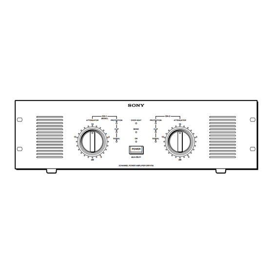
EXTERNAL DIMENSIONS NAMES AND FUNCTIONS OF PARTS Front Panel CHANNEL 1 7 Vents CHANNEL 2 (Monaural) OH-1 OH-2 (MONO) 3 PROTECTION Indicator ATTENUATOR PROTEOTION OVER HEAT PROTEOTION ATTENUATOR CLIP MONO CLIP 1 CLIP Indicator SIGNAL SIGNAL 5 ATTENUATOR Knob POWER 8 SIGNAL Indicator 2CHANNEL POWER AMPLIFIER SRP-P26 6 POWER Switch and Pilot Lamp... - Page 4 NAMES AND FUNCTIONS OF PARTS NAMES AND FUNCTIONS OF PARTS NL4 and Power amplifier internal wiring Rear Panel CH-1 1 INPUT 1 (MONO) Terminals (CH-1) – 2 INPUT 2 Terminals (CH-2) – INPUT OUTPUT OPERETION CH-2 CH-1 CH-2 MONO CH-1 (MONO) STEREO 3 OPERATION Switch...
- Page 5 CONNECTION Before Connecting How to Connect Cords Power Supply • Insert plugs completely or problems may result. Take the following precautions to prevent damage to the equipments used and the circuit breaker (safety device) • Disconnect cords by the plug. from turning ON.
-
Page 6: Disassembly
SECTION 2 DISASSEMBLY Note: Follow the disassemblly procedure in the numerical order given. CASE, UPPER 2 two screws 1 two screws (M 3 × 8) y (STEP TAPPING) 1 two screws y (M 3 × 8) 2 two screws y (STEP TAPPING) FRONT PANEL 2 two screws (BVTT 3 ×... -
Page 7: Ps Board
PS BOARD 4 connectors (CN801, 811) 5 screw (BVTT 3 × 10) 4 connectors 1 two screws (BVTP 3 × 16) (CN851, 852, 861) 2 collar, upper 1 two screws (BVTP 3 × 16) 4 connectors (CN871, 872) 2 collar, upper 6 two screws (BVTP 3 ×... -
Page 8: Sp/Input/Jack/Boards
SP/INPUT/JACK BOARDS 4 SP board 9 INPUT board 3 connector (CN603) ∗ unsolder 8 connectors (CN403, 411, 453, 491) 1 six screws 2 three screws 7 JACK board (BVTP 3 × 10) (BVTP 3 × 10) 5 four screws (BVTP 2.6) 6 four screws (BVTT 3 ×... -
Page 9: Electrical Adjustment
SRP-P26/P15 SECTION 3 SECTION 4 ELECTRICAL ADJUSTMENT DIAGRAMS 4-1. BLOCK DIAGRAM Note: Make adjustment at least 5 minutes after the POWER switch was turned ON. CLIP-1 SIGNAL-1 Bias Adjustment/DC Offset Confirmation CH-1 CH-1 Preparation: (MONO) OUTPUT ATTENUATOR nob : ∞ (MIN) INPUT PROTECTION-1 OVER HEAT... -
Page 10: Printed Wiring Board - Main/Input/Jack/Sp/A-Class/Vol1/Vol2 Boards
SRP-P26/P15 4-2. PRINTED WIRING BOARD - MAIN/INPUT/JACK/SP/A-CLASS/VOL1/VOL2 BOARDS - • Semiconductor Location Ref. No. Location D111 D112 D211 D212 D301 D302 D401 D402 D403 D404 D451 D452 D453 D454 D511 D512 D561 D562 D601 C-15 D602 C-15 IC401 IC402 IC451 C-10 IC452 C-10... -
Page 11: Circuit Diagram - Main/Input/Jack/Sp/A-Class/Vol1/Vol2 Boards
SRP-P26/P15 4-3. CIRCUIT DIAGRAM - MAIN/INPUT/JACK/SP/A-CLASS/VOL1/VOL2 BOARDS - NOTE: • All capacitors are in µF unless otherwise noted. pF : µF. 50V or less are not indicated except for electrolytics and tantalums. • All resistors except chips are in Ω and W or less unless otherwise specified. -
Page 12: Printed Wiring Board - Ps/Led/Sw/T1/T2/Th Boards
SRP-P26/P15 4-4. PRINTED WIRING BOARD - PS/LED/SW/T1/T2/TH BOARDS - • Semiconductor Location Ref. No. Location D701 D702 D703 D704 D705 D706 D707 D708 D709 D801 I-10 D802 D811 G-10 D812 G-10 D813 G-10 D814 G-10 D821 D822 D823 D824 D825 D826 D841 D842... -
Page 13: Circuit Diagram - Ps/Led/Sw/T1/T2/Th Boards
SRP-P26/P15 4-5. CIRCUIT DIAGRAM - PS/LED/SW/T1/T2/TH BOARDS - NOTE: • All capacitors are in µF unless otherwise noted. pF : µF. 50V or • Voltage is measured with respect to ground under no-signal less are not indicated except for electrolytics and tantalums. conditions. -
Page 14: Repair Parts List
* 11 2-346-111-01 COLLAR (LOWER) * 52 2-346-111-01 COLLAR (LOWER) * 62 1-666-721-21 TH BOARD (P26) 4-942-568-01 EMBLEM (NO.5), SONY * 12 1-666-718-11 VOL1 BOARD * 53 2-346-110-01 COLLAR (UPPER) * 63 A-4588-999-A COMBINED MAIN BOARD COMPLETE (P15) 2-335-846-01 ESCUTCHEON... -
Page 15: Rear Panel Section
5-3. REAR PANEL SECTION • B : INPUT board CP901 J611,612,613 supplied M901 supplied • B supplied Ref. No. Part No. Description Remarks * 101 2-346-140-01 FRAME (L) 2-337-554-01 FOOT * 103 2-346-141-01 FRAME (R) * 104 1-666-717-11 JACK BOARD * 105 2-346-104-01 PANEL, BACK * 106... -
Page 16: Main Board
SECTION 6 MAIN ELECTRICAL PARTS LIST Note: • Due to standardization, replacements in the • RESISTORS When indicating parts by reference number, parts list may be different from the parts All resistors are in ohms. please include the board name. specified in the diagrams or the components METAL: metal-film resistor used on the set. - Page 17 MAIN Ref. No. Part No. Description Remarks Ref. No. Part No. Description Remarks Q217 8-729-010-97 TRANSISTOR 2SC3856-Y (P26) R211 1-259-444-11 CARBON 4.7K 1/6W Q218 8-729-010-98 TRANSISTOR 2SA1492-Y (P26) R212 1-259-424-11 CARBON 1/6W Q219 8-729-010-97 TRANSISTOR 2SC3856-Y (P26) ! R213 1-219-177-91 FUSIBLE 1/2W F ! R214 Q219...
- Page 18 MAIN Ref. No. Part No. Description Remarks Ref. No. Part No. Description Remarks < VARIABLE RESISTOR > < DIODE > RV101 1-238-597-11 RES, ADJ, CARBON 1K D801 8-719-302-38 DIODE RBV-602-01 (P15) RV201 1-238-597-11 RES, ADJ, CARBON 1K D801 8-719-060-53 DIODE RBV-2506 (P26) ************************************************************ D802...
- Page 19 A-CLASS Ref. No. Part No. Description Remarks Ref. No. Part No. Description Remarks ! R824 1-219-165-11 FUSIBLE 1/2W F < RESISTOR > R851 1-259-468-11 CARBON 1/6W R852 1-259-468-11 CARBON 1/6W R511 1-259-428-11 CARBON 1/6W R853 1-259-468-11 CARBON 1/6W R512 1-259-476-11 CARBON 100K 1/6W R854...
-
Page 20: Input Board
INPUT JACK Ref. No. Part No. Description Remarks Ref. No. Part No. Description Remarks 1-666-721-11 TH BOARD (P15) < IC > ********* IC401 8-759-634-51 IC M5218AP 1-666-721-21 TH BOARD (P26) IC402 8-759-634-51 IC M5218AP ********* IC451 8-759-634-51 IC M5218AP IC452 8-759-634-51 IC M5218AP <... - Page 21 JACK VOL1 VOL2 Ref. No. Part No. Description Remarks Ref. No. Part No. Description Remarks < TERMINAL > < JACK > TM481 1-694-335-11 TERMINAL BOARD (INPUT CH-1) J611 1-774-508-11 CONNECTOR, SPEAKER (NL4MP) TM482 1-694-335-11 TERMINAL BOARD (INPUT CH-2) (OUTPUT CH-1) ************************************************************ J612 1-774-508-11 CONNECTOR, SPEAKER (NL4MP)
-
Page 22: Accessories And Packing Materials
7-685-874-09 SCREW +BVTT 3X12 (S) The components identified by mark ! or dotted line with mark ! are critical for safety. Replace only with part number specified. English 97G1601-1 Printed in Japan Sony Sound Tec Corporation 9-977-957-11 © 1997.7 — 30 —...
Need help?
Do you have a question about the SRP-P15 AEP and is the answer not in the manual?
Questions and answers