Table of Contents
Advertisement
Advertisement
Table of Contents

Related Manuals for BBK DK1440SI


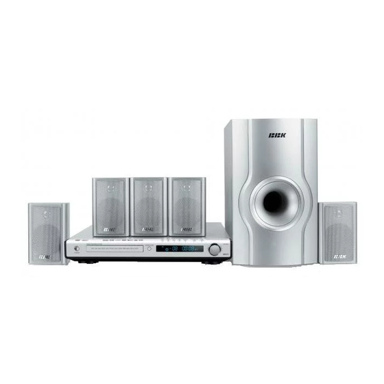
Summary of Contents for BBK DK1440SI
- Page 1 DK1410SI DK1440SI DK1470SI DK1480SI service manual...
-
Page 2: Table Of Contents
Catalog Chapter One About Maintenance 1.1 Safety precautions 1.1.1 Power supply 1.1.2 Precautions for antistatic 1.1.3 Precautions for laser head 1.1.4 About placement position 1.2 Maintenance method 1.2.1 Visualized method 1.2.2 Electric resistance method 1.2.3 Voltage method 1.2.4 Current method 1.2.5 Cutting method 1.2.6 Element substitution method 1.2.7 Comparison method... - Page 3 2.3.7 Preference settings 2.3.8 Parental control 2.3.9 Initial setup menu 2.3.10 Reset to defaults 2.3.11 Exit settings menu 2.3.12 Channel delay set-up Chapter Three Principle and Servicing Section One Principle of the Player 3.1.1 Function introduction 3.1.2 Block diagram principle of the player Section Two Unit Circuit Principle 3.2.1 Decode circuit 3.2.2 Servo circuit...
- Page 4 3.5.8 Function introduction to SAA6588 3.5.9 Function introduction to Cs5340 3.5.10 Function introduction to 4558/4580 3.5.11 Function introduction to TLV272 3.5.12 Function introduction to TAS5508 3.5.13 Function introduction to TAS5112 3.5.14 Function introduction to 5L0380 3.5.15 function introduction to LM431A 3.5.16 Function introduction to Hs817 3.5.17 Function introduction to Pt2579 Chapter Four Disassembly and Assembly Proces...
-
Page 5: Chapter One About Maintenance
Chapter One About Maintenance 1.1 Safety precautions 1.1.1 Power supply When maintenance personnel are repairing DVD players, he should pay special attention to power board with 220V AC and 330V DC which will cause hurt and damage to persons! 1.1.2 Precautions for antistatic Movement and friction will both bring static electricity which causes serious damages to integrated IC. -
Page 6: About Placement Position
1.1.4 About placement position 1. Never place DVD player in positions with high temperature and humidity. 2. Avoid placing near high magnetic fields, such as loudspeaker or magnet. 3. Positions for placement should be stable and secure. 1.2 Maintenance method 1.2.1 Visualized method Directly view whether abnormalities of collision, lack of element, joint welding, shedding welding, rosin joint, copper foil turning up, lead wire disconnection and elements burning up among pins of... -
Page 7: Element Substitution Method
1.2.6 Element substitution method When some elements cannot be judged good or bad, substitution method may de adopted directly. 1.2.7 Comparison method A same good PC board is usually used to test the correct voltage and waveform. Compared these data with those tested through fault PC board, the cause of troubles may be found. Through the above maintenance method, theoretical knowledge and maintenance experience, all difficulties and troubles will be readily solved. -
Page 8: Chapter Two Functions And Operation Instructions
Chapter Two Functions and Operation Instructions 2.1 Features Formats: Digital video playback of DVD-Video, Super VCD and VCD formats. MPEG-4 compatibility:Playback of Divx 3.11, Divx 4, Divx 5, Divx pro and XviD formats. Playback of music discs in DVD-Audio format. Playback of musical compositions in DC-DA and HDCD formats. -
Page 9: Controls And Functions
Auto protecion of TV screen. Child lock, parental control(protection against playing undesirable discs) Auto voltage selection(~110-250V)and short-circuit protection. 2.2 Controls and functions 2.2.1 Front panel controls STANDBY/POWER button SOURCE button Press to switch the device on/into standby. Press to switch between DVD-receiver/Audio Disc tray input/Tuner/Digital audio input. -
Page 10: Vfd Display General View
Center speaker input (output form the build-in S-Video output amplifier) SCART-type AV connector Subwoofer input (output from the build-in Coaxial digital audio output amplifier) Optical digital audio output Left Surround speaker input (output from the Optical digital audio input build-in amplifier) Coaxial digital audio input 2.2.3 VFD display general view MP3-disc... - Page 11 SKIP/RESET +/- Press to switch between files on disc/tuned radio stations A-B buttons Press to repeat the selected portion REPEAT button Press to repeat playback CH+/CH- button Press to change the acoustic channel MUTE button Press to change the acoustic channel VOLUME+/- button Press to adjust the volume SLOW button...
-
Page 12: Function Settings
# Default option: English 2.3 FUNCTION SETTINGS 2.3.1 Function selection and change Press the SETUP key to show the setup menu. You will see the following image on the screen, as shown on the figure: Select the 2.DVD-menu: Selection of disc menu language. desired menu item using the jog Dial;... -
Page 13: Sound Settings Menu
3.TV Format: image ratio settings Options: Front F, Center C, Surround Sr, Options: 4:3 pan&scan, 4:3 letterbox and 16:9 Subwoofer SW. Default options: Front F, Subwoofer SW. Default option: 4:3 pan & scan. If you want the low-frequency component of some discs are recorded with support of only the sound signal enter only the subwoofer one ratio. -
Page 14: Playback Settings
a) SPDIF format: set-up of digital audio output If on option is set, while reproducing discs, a options. menu will appear, in which you can select the Options: RAW, PCM or order of playing the disc content. If the off When you select the RAW option, the not option is wet, the reproducing of content is decoded signal is sransferred to the DVD... -
Page 15: Parental Control
# Default option: Off. 2.3.10 Reset to defaults Resetting all settings and restoring default options, except age restrictions level and password. Default option: Off. 2.Background: selection of an image as TV screen wallpaper. Options: Standard, Saved Default option: Standard. 2.3.11 Exit settings menu 3.Screen saver: Screen saver on/off. - Page 16 “Night” mode The Dolby Digital system provides an extremely broad dynamic range of playback sound-from gentle to roaring. It creates the presence effect, especially while seeing motion pictures. However, at night a powerful sound with a broad dynamic range may give pleasure to you, but disturb and annoy your family and neighbors.If you just decrease the volume, you will immediately notice that you ceased to hear,...
- Page 17 Creates an optimum sound field with The most cost-efficient way to illusion of an equal distance from ensure high-quality surround listener to each speaker effect Allows adjusting the decompression Surround sound may be received dagree of sound information("night" from any signal source. mode) Possibility of program mable control of Miscellaneous...
-
Page 18: Chapter Three Principle And Servicing
Chapter Three Principle and Servicing Section One Principle of the Player 3.1.1 Function introduction This players adopts new-generation DVD decode chip with built-in Dolby decoder, and the vivid surround system brings you to taste the living cinema effect. It has the following features: Progressive scanning output to produce steadier and clearer pictures without flickering Composite video, S-video and component video output Digital picture adjustment to sharpness, brightness, contrast, chroma and saturation of pictures,... - Page 19 Optial SCART Video S-video Coaxial Filtering Front Rear Rear Front Woofer Center Filtering AUXR External audio input AUXL Amplifying circuit N8 TAS5112 TAS5112 N9 TLV272 Tuner MIC 1 Amplifying circuit Microphone M 4558 N12 TAS5508 RC4580 RC4580 MIC 2 SDA AD DAVNIN SDATA0 SDATA1...
-
Page 20: Section Two Unit Circuit Principle
Section Two Unit Circuit Principle 3.2.1 Decode circuit 1. Decode circuit block diagram is shown as in the following figure 3.2.1.1: SDCLK SDCKE DRAS MT 1389 A0~A20 SDRAM FLASH DQM0 AD0~AD7 DQM1 DQ0~DQ15 URST MA0~MA11 1.8V Reset EEPROM voltage Clock circuit regulating 24C02... -
Page 21: Servo Circuit
Whether detect switch has been closed, if not, the door close action is performed. After detect switch of door is closed, the machine begins to perform preparations of disc reading and performs panel display at the same time of working. Playback process: laser head picks up disc signal from disc, after servo system processing, then send to decode circuit for decoding, signal after being decoded is saved in SDRAM for the moment. - Page 22 2. Working principle: After powering on or closing to proper position (on loader frame for general DVD player, on PCB board of below part of card door for PDVD player), loader lens begins to reset; after laser head is on proper position, detect switch will give a signal to MT1389, MT1389 begins to output focus, main axis and light emission signals, disc begins to rotate, laser head begins to recognise disc information, and judges whether disc is CD or DVD according to disc information to facilitate to output level from IOA pin...
-
Page 23: Laser Power Control Circuit
Deviation, now laser head is required to adjust. In this process, the object lens moves forwards or Backwards, and the moving range is very small. (3) FMO: similar to acts of trace, the acts of feed are larger than those of trace. Feed conducts a large scale movement firstly, and then trace moves slightly in this range. -
Page 24: Main Axis Control Circuit
When reading DVD disc, pin 21 is detect signal input pin, pin 22 is drive control input pin, and the working principle is the same with that when playing VCD disc. 3. Key point voltage (unit: V) is shown as the following table: When reading When no Name... -
Page 25: Control Panel Circuit
3. Working principle: MT1389 has a comparator inside composed of operational amplifier, in which OP+ is the in-phase input end of operational amplifier, OP- is reverse input end, OPO is output end, when playing disc normally, for electric machine is positive direction rotating, voltage of OP+ is higher than that of OP-, voltage of OPO is more than 1.4V. -
Page 26: Power Circuit
2. Working principle (1) Realization of button function: when users are operating machine, button matrix circuit will produce a button information, and recognise button through S0793 to produce button function code to transmit to the main CPU inside decode chip, CPU performs the corresponding switch to the function module inside system, and a signal will produce to control OSD and panel display part to make the corresponding display. - Page 27 2. Working principle: this power circuit is composed of two parts, which use the common electromagnetic interference filtering circuit and bridge rectification circuit and filtering circuit. The first part circuit produces P+28V DC used to supply power for power amplifier circuit; the other part is responsible for the power supply of other module circuit of the player.
-
Page 28: Audio Power Amplifying Circuit
2.5V (means output voltage is on low side), LM431 cuts off, the “on” time of VEPR22 increases, output voltage increases, thus power board outputs stable voltage through the auto control function of feedback loop. (9) Filtering circuit: the function is to produce a stable and small-ripple DC voltage. “ “-style filter is often adopted in filtering circuit. - Page 29 2. Working principle: the system switches DVD signal and external input signal through the control of N3, N4 by M0, M1. When M0, M1 is 0, 1, through the selection of DVD signal bu system, N3B, N3C, N3D, N4A, N4B, N4C of tri state gate buffer open, N3A and N4D close, 1389 sends the digital audio signals SDA_LR, SDA_SLSR, SDA_SCW, SCLK, LRCK to 5508 directly for formatting, and the system clock MCLK of power amplifier board is provided by 1389 through pin 6 of XP207, after being converted by CS5340 AD , MIC signals are directly sent inside 1389 for processing, and overlapped to left/right...
-
Page 30: Output Circuit
3.2.8 Output circuit 1. Power amplifier surround left and right channel block diagram is shown in the following figure 3.2.8.1: SDATA1 ASDAT1 Disc MT1389 R295 XS207 Loader N3 74HCT125 PWMSR+ SROUT PWMSR- 6DASLSR R100 XC100 TAS5508 PWMSL+ TAS5112 SLOUT PWMSL- Figure 3.2.8.1 Power amplifier surround left and right channel block diagram 2. - Page 31 3. Microphone circuit block diagram is shown in the following figure 3.2.8.3: MIC2 C210 R12 XS201 XP204 4558 C110 R12 CS5540 MIC1 CD4052 ASDATO XS207 U201 R101 L351 Xs207 power MT1389 amplifier board FLOUT PWM FL+ PWM FL- TAS5112 PWM FR- PWM FR+ FROUT PWM RL- LOUTX...
-
Page 32: Video Circuit
5. External input circuit block diagram is shown in the following figure 3.2.8.5: AUXR L122 R225 XS401 CD4052 CS5340 AUXL L121 SDIN3 FLOUT PWM FL+ PWM FL- TAS5112 PWM FR- PWM FR+ FROUT PWM RL- LOUTX L100 R166 R165 C108 R217 PWM RL+ XS401... - Page 33 2. On the basis of 1389B, 1389E uses some pin functions again, and reduces USB function, so it shows concise, video output pin is used again, the brightness signal, chroma signal, CVBS signal and component video signal decoded through U201 (MT1389), through low pass filtering and clipping, are sent to the corresponding terminal for output, shown in the figure 3.2.9.2: XS206 L376...
-
Page 34: Section Three Servicing Cases
Section Three Servicing Cases 3.3.1 Servicing cases Example 1 Mixed left channel on AV board has no sound Analysis and troubleshooting: Step 1: use oscillograph to test LO signal on pin 5 of XS401 on power amplifier board and find that there is no signal, after unplugging flat cable on XS401, LO still has no signal output, so we can confirm that trouble lies in power amplifier board. - Page 35 Output, then when checking pin 4 of N7, there is no signal output, use multimeter to test whether circuit between N5 and N7 is connected and also no trouble is found. After changing N7 (CS5340), trouble is removed. 1. External L/R N13\N14 Output channel input...
- Page 36 Step 5: use DC level of multimeter to test voltage on output terminal, and find that voltage of SW+ and SW- is 6.09V, voltage of all other output is 14.02V and they are both +14V in normal conditions, so we can judge that the capacitor of circuit between N13 (TAS5112) and output part has electric leakage, change C139, C140, C141, C142, C143, C66, C71, but trouble is still not removed.
- Page 37 Test the resistance to ground of HDET signal of pin 7 of XS207 and it is 0 ohm, and it should be infinite in normal conditions, so we preliminarily confirm that HDET signal is short-circuited to ground, unplug flat cable on XS201, test the resistance to ground of pin 7 of XS201 and it is infinite, which is normal, and now test the resistance to ground of pin 7 (HDET) of XP204 on panel and it is still 0 ohm, so we can consider that problem lies in main panel, headphone board or flat cable, unplug the flat cable between panel and headphone, test the resistance to ground of pin 7 of XP204 on panel and it is infinite, so we...
- Page 38 Example 9 Power not on Analysis and troubleshooting: Step 1: check power supply of power board and find that power has no voltage output, unplug flat cable on power board and there is still no voltage output on power board, so we can confirm that trouble lies in power board.
- Page 39 Example 11 Component color distortion Analysis and troubleshooting: Step 1: check MT1389 clock, 26.999MHZ, VPP=1.72V, normal (27KHZ when in normal conditions). Step 2: check MT1389 power supply and it is normal. Step 3: use oscillograph to test the 3 component signals of pin 6 (Y4), pin 7 (Y5) and pin 8 (Y6) of XP206 on AV board and they all have output, but when using multimeter to test DC voltage of the 3 signals, we find that Y5 has +4.7V, in normal conditions, this voltage should be two several tenths of a volt and one volt plus a little at most.
- Page 40 Example 14 Not read DVD Analysis and troubleshooting: Step 1: check XS301 socket and flat cable and no abnormality is found (you may observe directly, and you need to insert it again when you find that flat cable is loose). Step 2: change loader and trouble is removed.
- Page 41 Example 17 No disc reading Analysis and troubleshooting: shown in the figure 3.3.1.5, Step 1: check the nerve flat cable socket on XS301 and find no abnormality. Step 2: change loader, disc reading is normal and trouble is removed. U301 BA5954 Figure 3.3.1.5 Servo drive circuit diagram Example 18 No disc reading...
-
Page 42: 2Troubleshooting Flow Chart
3.3.2Troubleshooting flow chart 1. Troubleshooting process for voltage too high or too low is shown as the following figure 3.3.2.1: Voltage too high or too low Only one output too high or too low Multiple outputs too high or too low Change Check Check whether filter... - Page 43 2. Troubleshooting process is shown as the following figure 3.3.2.2: Trouble when opening/ closing disc tray Opening disc Close disc tray Disc tray Open disc tray Open/close disc Disc tray Noise occurs in automatically tray automatically not open not close automatically tray not fully disc tray door...
- Page 44 3. URST# is always high level troubleshooting process, shown in the figure 3.3.2.3: RST# is always high level. Forced reset firstly Whether the player Check other circuit. works normally. Change phase inverter Change Q320 and check whether U205 (HCU04) is normal. Check whether R2023 is short circuit;...
- Page 45 4. Troubleshooting process for “On-screen-mosaic when playing” is shown as the following figure 3.3.2.4: On-screen-mosaic when playing Check whether power Refer to troubleshooting supply and clock signal process of U201 (MT1389) of U201 (MT1389) is normal power supply and clock circuit Change U201 Change U208 (SDRAM) Change U207 (FLASH)
- Page 46 5. Troubleshooting process for “No output for composite video” is shown as the following figure 3.3.2.5: No output for composite video signal Whether U201 (MT1389) Whether it is normal 1. Check power supply circuit Whether Y3 has video power supply and crystal after restoring into 2.
- Page 47 6. Troubleshooting process for "No colour of picture" is shown as the following figure 3.3.2.6: No colour of picture Check whether clock Check clock circuit signal is normal Check power supply circuit Check whether U201 (refer to MT1389 (MT1389) is normal troubleshooting flow chart) Change MT1389 Check other circuit...
- Page 48 7. Troubleshooting process for no sound of power amplifier board when playing is shown as the following figure 3.3.2.7 No sound in power amplifier Check whether flat cable holder is joint board when playing disc welding or inserted to proper position No sound for a certain channel No sound output for all (take centre sound for instance)
- Page 49 8. Troubleshooting process for no sound of MIC is shown as the following figure 3.3.2.8: No sound of MIC One has no sound, for instance, Both have no sound MIC1 has no sound Check whether Whether MIC item Check XP201, XS201 and Use remote controller to pin 3 of XS201 has flat cable or change MIC...
- Page 50 9. Troubleshooting process for no sound of headphone is shown as the following figure 3.3.2.9 No sound of headphone Insert headphone Whether pin 7 HDET Whether pin 6 HDET Change headphone holder of Xs201 is low level of XS106 is low level Check flat cable of XS106, XP106 Whether power...
- Page 51 10. Troubleshooting process for no echo of microphone is ahown as the following figure 3.3.2.10 No echo Check Check whether DET 1. Check whether R618 has whether pin 7 of N1 (4558) has a voltage that changes with open circuit or variable value has a voltage that changes with microphone volume change microphone volume...
- Page 52 11. Troubleshooting process for no remote control function is shown as the following figure 3.3.2.11 No remote control function (remote controller is normal) When pressing Check whether remote controller, use Check the relevant power oscillograph to check 5V power supply of pin 3 supply circuit whether pin 1 of flat of N103 (REMOT)
- Page 53 12. Troubleshooting process for there is sound but no image is shown as the following figure 3.3.2.12 There is sound but no image One path has no output Each path signal has no output Whether the corresponding pin of MT1389 has output Check whether Check power supply circuit...
- Page 54 13. Troubleshooting process for no screen display is shown as the following figure 3.3.2.13 No screen display Check whether Check the corresponding voltage of pin 3, 4 of XP505 is normal. FL+ is -16V power supply circuit and FL- is -19V.
- Page 55 14. Troubleshooting process for power supply output power not enough is shown as the following figure 3.3.2.14 Output power of power supply is not enough Only one channel’s output power of power supply is not enough Change this channel Change filter capacitor rectification diode Several channels’...
- Page 56 15. Troubleshooting process for image distortion is shown as the following figure 3.3.2.15 Image distortion Check clock circuit Composite video signal Component video distortion All video outputs distortion distortion Check whether catching Check whether there is one Recover factory settings Note diode VD214 is normal path output in three paths...
- Page 57 P+28V voltage trouble +28V voltage is on high or low side +28V voltage has no output Check Check whether pin 1 Check Check whether TC501, 1. Check whether TC508 is normal. of U505 (KAIM0880) whether cathode whether pin 1 bridge rectifier module 2.
- Page 58 No voltage output Several paths have no voltage output Only one path has no voltage output Check whether filter capacitor Find which path has no output Check Each path has no voltage output Change has electric leakage Check whether whether cathode DV505 and C509, TC508, TC509 board of D505 has 3.3V...
- Page 59 No sound for external input 1. Whether pin 20 of XS207 is high level (3.3V) 2. Whether V5 and V6 are normal All external outputs No sound for tuning 3. Check other peripherical have no sound circuit of TV6 No sound for external mixed left and right channels Change N5 Check whether...
- Page 60 Power not on Check Unplug Unplug whether voltage X203 flat cable Output power of power supply Whether X203 flat cable, of pin 7 (5), pin 4 (3.5V) and test whether resistor of this path is not enough test on power board and each path output is and pin 11 (5V) of to ground of decode board...
- Page 61 Check whether the place of XS301, XS303, XS302 is well No disc reading inserted or oxidated Check Change loader whether power and check whether it is Check power supply circuit supply of pin 8 and 7 of normal U302 (D5954) is 5V Check Check...
-
Page 62: Section Four Servicing Parameters
Section Four Servicing Parameters 3.4.1 Signal waveform diagram This section collects signal waveform diagram of audio, video and each unit circuit with the purpose to help servicing personnel to judge where trouble lies in accurately and quickly to improve servicing skills. - Page 63 3. 1389 main clock signal waveform diagram 4. Contrast figure of TAS5508 reset signal RST and main reset signal URST#, USRT# means the time required to finish reset is 600ms, RST means reset begins and time is 680ms 5. Waveform of PWM signal outputted by TAS5508 when playing: f=352.78KHZ - 59 -...
- Page 64 6. PWM_RL signal, output range is 4.0V, frequency is 384.0KHZ (fixed output does not change with volume adjustment), waveform of two ends of R103 7. When in external input, main clock of TAS5508 (waveform diagram of pin 4 of N2) 8.
-
Page 65: Key Point Voltage
3.4.2 Key point voltage 1. Voltage of key point is shown as follows: When reading disc When no disc Name When disc out When disc in normally There is about 1 second 3.3V pulse TROPEN when at the moment of disc out There is about 1 second 3.3V pulse when at TRCLOSE the moment of disc out... - Page 66 4. Key point test point voltage (V) is shown as the following table: DC voltage when no Signal Function Troubles disc in (V) Brightness of S-VIDEO S-video without picture/picture bright/pict ure dark 0.74 Chroma of S-VIDEO S-video without color/color distortion 1.48 Composite video without picture/picture VIDEO...
-
Page 67: Section Five Function Introduction To Ic
Section Five Function Introduction to IC 3.5.1 function introduction to MT1389E 1. DESCRIPTION MT1389E is a cost-effective DVD system-on-chip (SOC) which incorporates advanced features like MPEG-4 video decoder, high quality TV encoder and state-of-art de-interlace processing. Based on MediaTek’ s world-leading DVD player SOC architecture, the MT1389E is the 3rd generation of the DVD player SOC. - Page 68 Versatile video scaling & quality enhancement OSD & Sub-picture Built-in clock generator Built-in high quality TV encoder Built-in progressive video processor Audio effect post-processor Built-in 5.1-ch Audio DAC Built-in 2-ch Audio ADC for Karaoke (2)High Performance Analog RF Amplifier Programmable fc Dual automatic laser power control Defect and blank detection RF level signal generator...
- Page 69 Supports 5/3.3-Volt. FLASH interface Supports power-down mode Supports additional serial port (7)DVD-ROM/CD-ROM Decoding Logic High-speed ECC logic capable of correcting one error per each P-codeword or Q-codeword Automatic sector Mode and Form detection Automatic sector Header verification Decoder Error Notification Interrupt that signals various decoder errors Provide error correction acceleration (8)Buffer Memory Controller Supports 16Mb/32Mb/64Mb SDRAM...
- Page 70 High Definition Compatible Digital (HDCD) Windows Media Audio (WMA) Dolby ProLogic II Concurrent multi-channel and downmix out IEC 60958/61937 output PCM / bit stream / mute mode Custom IEC latency up to 2 frames Pink noise and white noise generator Karaoke functions Microphone echo Microphone tone control...
- Page 71 4. PIN DESCRIPTION Main Type Description RF interface (26) RFGND18 Ground Analog ground RFVDD Power Analog power 1.8V Analog output RF Offset cancellation capacitor connecting Analog output RF Offset cancellation capacitor connecting RFGC Analog output RF AGC loop capacitor connecting for DVD-ROM Current reference input.
- Page 72 LDO2 Analog output Laser driver output LDO1 Analog output Laser driver output Reference voltage (3) V2REFO Analog output Reference voltage 2.8V Analog output Reference voltage 2.0V VREFO Analog output Reference voltage 1.4V Analog monitor output (7) SVDD3 Power Analog power 3.3V Central servo RFOP Analog output...
- Page 73 LPFIN Analog input Negative input terminal of loop filter amplifier LPFOP Analog output Positive output of loop filter amplifier Motor and Actuator Driver Interface (10) OP_OUT Analog output Op amp output OP_INN Analog input Op amp negative input OP_INP Analog input Op amp positive input Analog output Disk motor control output.
- Page 74 SRPU InOut 4~16mA, HIGHA2 Microcontroller address 10 SRPU InOut 4~16mA, HIGHA3 Microcontroller address 11 SRPU InOut 4~16mA, HIGHA4 Microcontroller address 12 SRPU InOut 4~16mA, HIGHA5 Microcontroller address 13 SRPU InOut 4~16mA, HIGHA6 Microcontroller address 14 SRPU InOut 4~16mA, HIGHA7 Microcontroller address 15 SRPU InOut 4~16mA, Microcontroller address/data 7...
- Page 75 InOut 4~16mA, IOA 4 Microcontroller address 4/ IO SRPU InOut 4~16mA, IOA 5 Microcontroller address 5/ IO SRPU InOut 4~16mA, IOA 6 Microcontroller address 6/ IO SRPU InOut 4~16mA, IOA 7 Microcontroller address 7/ IO SRPU InOut 4~16mA, Flash address 16 SRPU InOut 4~16mA, Flash address 17...
- Page 76 InOut 4mA, UP1_3 Microcontroller port 1-3 SRPD,SMT InOut 4mA, UP1_4 Microcontroller port 1-4 SRPD,SMT InOut 4mA, UP1_5 Microcontroller port 1-5 SRPD,SMT InOut 4mA, 9) Microcontroller port 1-6 UP1_6 SRPD,SMT 10) I2C clock pin InOut 4mA, 11) Microcontroller port 1-7 UP1_7 SRPD,SMT 12) I2C data pin InOut 4mA,...
- Page 77 I) Alternate digital video YUV output 0 II) GPIO 8) Audio serial data 0 (Front-Left/Front-Right) 9) Trap value in power-on reset: I) 1: manufactory test mode YUV2 InOut 4mA, ASDATA0 II) 0: normal operation PD,SMT 10) While internal audio DAC used: I) Digital video YUV output 2 II) GPO 11) Audio serial data 1 (Left-Surround/Right-Surround)
- Page 78 AKIN2 Analog Audio ADC input 2 ADVCM Analog 2ch audio ADC reference voltage AKIN1 Analog Audio ADC input 1 AADVDD Power 3.3V power pin for 2ch audio ADC circuitry APLLVDD3 Power 3.3V Power pin for audio clock circuitry APLLCAP Analog InOut APLL external capacitance connection APLLVSS Ground...
- Page 79 DACVDDB Power 3.3V power pin for video DAC circuitry DACVSSB Ground Ground pin for video DAC circuitry DACVDDA Power 3.3V power pin for video DAC circuitry InOut 4mA, Green, Y, SY, or CVBS DACVSSA Ground Ground pin for video DAC circuitry InOut 4mA, B/CB/PB Blue, CB/PB, or SC...
- Page 80 InOut 4mA, 52) General purpose IO 7 GPIO7 YUV3 SR,SMT 53) Digital video YUV output 3 Dram Interface (38) (Sorted by position) InOut DRAM address 4 InOut DRAM address 5 InOut DRAM address 6 InOut DRAM address 7 InOu DRAM address 8 InOut DRAM address 9 RA11...
-
Page 81: Function Introduction To Sdram
InOut DRAM data 1 InOut DRAM data 2 InOut DRAM data 3 InOut DRAM data 4 InOut DRAM data 5 InOut DRAM data 6 InOut DRAM data 7 DQM0 InOut Data mask 0 3.5.2 Function introduction to SDRAM The function of SDRAM (U211) in the player is to save program taken out by MT1389 from FLASH and information of picture and sound taken out from disc when the player is working to form damping, add the stability of information output and add anti-vibration of the player. -
Page 82: Function Introduction To Flash
Data in/out screen-shielded LDQM 2.46 Data bus signal Write control signal 3.17 VDDQ 3.3V power supply 3.19 Line address gating signal 3.01 Data bus 0.91 Row address gating signal 3.13 DQ10 Data bus Chip selection signal 2.95 VSSQ Ground 0.01 Section address 0 gating... -
Page 83: Function Introduction To D5954
Take word extend mode as data line, and bit DQ15/A-1 extend mode as address line Select 8-bit or 16-bit output mode. High level is BYTE 16-bit output and low level is 8-bit output 3.5.4 Function introduction to D5954 D5954 is a servo drive IC with built-in 4-channel drive circuit. -
Page 84: Function Introduction To 24Llc020
PVCC2 5V power supply 5.38 5.08 5.07 PREGND Ground 0.01 0.01 VINLD Feed control signal input 1.41 CTK2 External feedback loop 2.41 2.52 2.53 CTK1 External feedback loop 2.51 2.52 2.53 VINTK Trace control signal input 1.42 1.42 1.41 BIAS 1.4V reference voltage input 1.41 1.42... -
Page 85: Function Introduction To 74Hct125
3. Pin function is shown as the following table: Name Voltage in actual test Name Voltage in actual test DC/NC 3.21 RST _/NC WP/RST 0.29 3.21 Note: when playing DVD, CD disc and no disc in, the measured voltage are all the same, in which pin 7 is protection-write pin, unused. - Page 86 Left/right channel digital audio gating signal SDATA0 Left/right channel digital audio signal input SDA LR Left/right channel digital audio signal output R101 Ground Ground SDA SLSR Surround left/right channel digital audio signal output R100 SDATA1 Surround left/right channel digital audio signal input Surround left/right channel digital audio gating signal SDA CSW Centre subwoofer digital audio signal output...
-
Page 87: Function Introduction To Cd4052
Function Remark Internal signal Disc signal, MIC signal 1(3.3V) External signal Tuner, external input unused unused 3.5.7 Function introduction to CD4052 Cd4052 is a 2-group 4-channel data selector used to select external input audio signal, microphone signal or tuner audio signal. 1. - Page 88 3.5.8 Function introduction to SAA6588 SAA6588 tuning data processing chip and pin function are shown as the following table: Data Data Name Function Remark Name Function Remark direction direction Multi-path rectifier output unused PSWN Pause switch output unused MPTH Multi-path detector output unused Attached address input...
- Page 89 # Auto mode selection # Compatible with CS5341 pin 3.Pin function of CS5340 is shown as the following table: Name Data direction Function Remark Mode selection Decide the operation mode of element Δ-δclock source of adjustor and digital filter MCLK Main clock Logic power supply Forward power supply of digital input/output...
- Page 90 3.5.11 Function introduction to TLV272 TLV272 includes two integrated operational amplifiers inside, with pin function shown as follows: Data Data Name Function Name Function direction direction 1OUT Output of operational amplifier A 2IN+ Output of operational amplifier B Negative input terminal of operational Negative input terminal of operational 1IN- 2IN-...
- Page 91 RESET TAS5508 reset signal HP-SEL Headphone/microphone selection bit Power failure control bit MUTE Mute control bit DVDD Digital 3.3V power supply DVSS Digital ground VR-DPLL Reference voltage of digital PLL power supply 1.8V OSC-CAP Oscillator capacitor connection end XTL-OUT Clock signal output XTL-IN...
- Page 92 PWM-P-2 Power amplifier right channel PWM output (positive end) PWM-M-3 Power amplifier surround left channel PWM output (negative end) PWM-P-3 Power amplifier surround left channel PWM output (positive end) PWM-M-4 Power amplifier surround right channel PWM output (negative end) PWM-P-4 Power amplifier surround right channel PWM output (positive end) ...
- Page 93 1. Function of each pin of N3 (TAS5112) is shown as follows: Name Data direction Function Remark Common Common GREG Door drive voltage regolator decoupling pin Chip over heat alarm output SD-CD Off label position of surround left/right channel Refer to table 3 SD-AB Off label position of subwoofer power amplifier...
- Page 94 BST-A High-side bootstrap supply(BST) PVDD-A Subwoofer negative end power supply PVDD-A Subwoofer negative end power supply OUT-A Subwoofer negative end output OUT-A Subwoofer negative end output Common Common ...
- Page 95 Chip over heat alarm output SD-CD Off label position of centre power amplifier Refer to table 3 SD-AB Off label position of left/right channel power amplifier Refer to table 3 PWM-DP Centre PWM positive signal input PWM-DM Centre PWM negative signal input RESET-CD Centre power amplifier reset signal...
- Page 96 Common Common OUT-B Left channel power amplifier output OUT-B Left channel power amplifier output PVDD-B Left channel power amplifier power supply PVDD-B Left channel power amplifier power supply BST-B High-side ...
- Page 97 5. Table 3 is shown as follows: RESET Function description none Device in protection mode Device set in high impedance state normal working 3.5.14 Function introduction to 5L0380 Pin 3 of 5L0380 is controlled by feedback pin 4 to make it on for a while and off for another while to form pulse DC to control coupling quantity of transformer.
- Page 98 Figure 3.5.15.1 LM431A outside drawing 3.5.16 Function introduction to HS817 U502 (HS817) is a photoelectric coupler, shown as the figure 3.5.16.1.The right side is a light emitting diode, which sends out light of different intensity according to the strength of voltage inputted from the right side, generates photocurrent of different intensity on the left side according to light of different intensity, and outputs from position D.
- Page 99 # Low Power Consumption # Anti-Aliasing Filter (2 Order) # Reconstruction Filter (2 Order) # 57kHz Band-Pass Filet (8 Order) # 57kHz Carrier Regeneration # Differential Decoder # Signal Quality Detector # Subcarrier Output Selectable 4.332 / 8.664 MHz Crystal Oscillator with Variable Dividers Synchronous Demodulator for 57kHz Modulated RDS Signals # Clocked Comparator with Automatic Offset Compensation # Clock Generation with Lock on Biphase Data Rate...
- Page 100 Chapter Four Disassembly and Assembly Process DVD players manufactured in BBK are largely identical but with minor differences and are mainly composed of loader components, control panel components, decode and servo board components, power board components, power amplifier board components, MIC board components and AV board components.
- Page 101 Chapter Cinque PCB board & Circuit diagram Section One PCB board 5.1.1 Surface layer of AV OUT Board XC106 C119 XC103 XC107 XC104 XC105 C117 R113 L116 XP206 V101 XP401 - 97 -...
- Page 102 5.1.2 Bottom layer of AV OUT Board - 98 -...
- Page 103 5.1.3 Surface layer of KEY SCAN Board VD102 R115 S100 S102 S103 S104 S105 S106 S101 VD104 R116C113 XS106 C112 VD101 VD103 N103 C111 CDVR938-4 C110 2004 11 19 R120 R122 C109 C108 VD105 C116 R123 R129 S107 R124 R127 R126 R121 DS100...
- Page 104 5.1.4 Bottom layer of KEY SCAN Board VD106 MIC100 VD107 MIC101 - 100 -...
- Page 105 5.1.5 Surface layer of DECODE&SERVO Board TC215 Q320 R2011 R2025 R2022 R2024 R229 R2023 L202 R231 C1003 XS203 XS207 L204 R230 C274 L352 SDATA0 L356 L350 SDATA1 L213 L355 SDATA2 L353 U213 L358 L351 L359 SACLK C266 L354 L373 L214 SBCLK R218 L361...
- Page 106 5.1.6 Bottom layer of DECODE&SERVO Board D215 C269 C267 C268 R303 L316 L205 C278 C226 Q303 C251 R311 C218 R209 R310 C252 C219 C253 C225 C242 C239 Q304 R210 C302 C230 C231 L201 C207 C282 R237 C2154 C237 C281 R236 C2155 L206 C208...
- Page 107 5.1.7 Surface layer of audio power amplifying Board XC100 R182 C170 R181 R177 R178 R176 R145 R197 R196 R51 R42 R187 R184 R50 R172 R192 R194 R43 R46 R183 R195 R193 R191 R143 R142 C185 XP503 XS402 R117 R119 C139 R120 R121 C205...
- Page 108 5.1.8 Bottom layer of audio power amplifying Board R224 R126 R125 R124 R123 - 104 -...
- Page 109 5.1.9 Power Board TC501 YC502 T502 C518 Designator20 TC516 TC515 U505 L506 C519 Designator19 TC517 C517 R522 TC513 ZD503 U506 TC514 RT501 C522 R523 U507 U504 TC505 C505 R517 TC504 D509 C504 YC501 D503 TC503 C508 TC507 C507 L504 C515 U501 D504 TC508...
- Page 110 耳机板 CDVR938-3 XS106 HGND VD107 C106 LEDDR DGND VD106 HDET Blue LED CON6 CKX-3.5-01K Blue LED DS100 HNV-08SS56 XP204 CON7 MIC2 AGND MIC1 HGND MIC101 MIC2 -21V HDET 1N4148 1N4148 1N4148 VD101 VD102 VD103 VD104 1N4148 MIC100 XP505 CON5 MIC1 D+5V DGND D+5V...
- Page 111 XC103B L102 ROUTX C102 MIX-out +12V D+5V LOUTX L100 C103 AGND AGND AUXR AUXL L120 VIDIO COMP XP401 C121 CON8 D+5V L119 VIDEO_C C122 VD109 XC103A 1N4148 L106 L118 XC105 VIDEO_Y DASW-02 L122 1.8uH VD108 R105 C123 1N4148 C106 C108 L121 AUX-in C118...
- Page 112 AVCC R308 R309 C219 391 JITFO JITFN 100K L316 89V33 LDO-AV33 L201 FBSMT R311 RFV18 FBSMT C318 C319 R209 750K Q305 C230 C231 C232 C233 C234 C235 3904-S R210 C223 TC206 C220 C217 R301 R310 20pF 10uF/16V TC204 100K LDO-AV33 C224 C218 4.7R...
- Page 113 R2026 33R(DNS) U208 R2027 33R(DNS) SDRAM 64M 89V33 89V33 ACLK R2004 SACLK R2005 ABCK SBCLK C254 U202 R2006 ALRCK SLRCK AT24C02 SDCKE ASDAT0 R2007 SDATA0 R232 R233 R2008 ASDAT1 SDATA1 DC/NC ASDAT2 R2009 SDATA2 RST_/NC RST/WP C295 WP/RST_ 20pF XS207 FBSMT L350 C2003...
- Page 114 +12V -12V C199 PWM_H_PR PWM_H_PR AUIN_SL1 AUIN_SL0 OUTPUT 4558 PWM_H_MR PWM_H_MR XS401 PWM_H_PL C200 PWM_H_PL +12V MIC(1) PWM_H_ML PWM_H_ML AUX(2) PWM_RR+ PWM_RR+ TUNER(3) PWM_RR- PWM_RR- -12V AGND +12V PWM_RL+ PWM_RL+ PWM_RL- PWM_RL- AGND PWM_SW+ PWM_SW+ AUXR PWM_SW- PWM_SW- AUXL PWM_CEN+ PWM_CEN+ R20 1K PWM_CEN-...
- Page 115 YC502 ~400V 102 DCVPP P-gnd R518 C518 P +28V U505 33R/1W R520 KA1M0880BTU TO-3P-5L R516 C516 R530 BYW29E200 D510 1K/3W R523 47K/2W 103/1KV 1.5K T502 C520 D511 BYW29E200 U506 D508 C521 R522 C523 R519 C522 ZD503 HER207 C519 4.7V 33R/1W U507 TC513 HS817...
- Page 116 Chapter six BOM List MATERIAL MATERIAL NAME SPECIFICATIONS LOCATION CODE DVD HOME THEATER DK1410SI(RU) POWER BOARD 5447883 2100017 LEAD F 0.6 SHAPED 20mm W1,W2 2100003 LEAD F 0.6 SHAPED 7.5mm W3,W7,W8,W9,W10 2100004 LEAD F 0.6 SHAPED 10mm W4,W5,R514 2100007 LEAD F 0.6 SHAPEN 15mm 0000274 CARBON FILM RESISTOR 1/4W47O±5% SHAPED 10...
- Page 117 MATERIAL MATERIAL NAME SPECIFICATIONS LOCATION CODE 0200138 PORCELAIN CAPACITOR 50V 104±20% 5mm C502,C514,C517,C521 0200224 PORCELAIN CAPACITOR 1000V 103 +80%-20% 7.5mm C501,C516 TEMETAL OXIDE FILM 0210158 100V 472±10% SHAPED 5mm C506,C508,C510,C515 RESISTORLENE CAPACITOR TEMETAL OXIDE FILM 0210024 100V 333±10% 5mm C505 RESISTORLENE CAPACITOR TEMETAL OXIDE FILM 0210148...
- Page 118 MATERIAL MATERIAL NAME SPECIFICATIONS LOCATION CODE 0570014 DIODE HER107 D501 0570042 DIODE HER207 SHAPED 12.5mm D508 0570045 DIODE BYW29E-200 TO-220 D510,D511 VOLTAGE REGULATOR 05800069 5.1V±5% 1/2W BELT ZD501 DIODE VOLTAGE REGULATOR 0580022 12V±5% 1W ZD502 DIODE 0570032 DIODE 1N5408 D512~D515 0880379 IC LM7805 GOLD SEALED TO-220 U504 ②...
- Page 119 MATERIAL MATERIAL NAME SPECIFICATIONS LOCATION CODE DVD HOME THEATER DK1410SI(RU) DECODE BOARD 2DK1410S-0 1.2Ver2.1 CMETAL OXIDE FILM 0960020 27.00MHz 49-S X201 RESISTORSTAL OSCILLATOR 14P 1.0mm DUAL RANK STRAIGHT 1940140 CABLE SOCKET XS207 INSERT 1940065 SOCKET 13P 2.0mm XS206 1940005 SOCKET 6P 2.0mm...
- Page 120 MATERIAL MATERIAL NAME SPECIFICATIONS LOCATION CODE 0090034 SMD RESISTOR 1/16W 100K±5% 0603 R210,R215,R308,R310 0100019 SMD RESISTOR NETWORKS 1/16W 33O±5% 8P RN201 0310085 SMD CAPACITOR 50V 20P±5% NPO 0603 C223,C295 0310190 SMD CAPACITOR 50V 27P±5% NPO 0603 C275,C276 0310045 SMD CAPACITOR 50V 47P±5% NPO 0603 C257~C259 0310047 SMD CAPACITOR...
- Page 121 ,TC301 MAGNETIC BEADS 03900579 RH354708 BELT L213~L216,L218,l219 INDUCTOR 03904299 INDUCTOR L204 330UH±10% 0410 BELT DVD HOME THEATER DK1410SI(RU) REMOTE CONEROL 5471746 0310222 SMD CAPACITOR 25V 104±20% X7R 0603 C3 ,C5 0310191 SMD CAPACITOR 50V 30P±5% NPO 0603 C1, C2 0090029 SMD RESISTOR 1/16W 47K±5% 0603...
- Page 122 CONDUCT GLUE OF REMOTE 4631059 RC-073 CONTROL(LOWER) GLUE BAG FOR ENVIRONMENTAL 5071274 85×290×0.05 PE PROTEETION(WITHOUT HOLE) DVD HOME THEATER DK1410SI(RU) EARPHONE BOARD 5446196 0310207 SMD CAPACITOR 50V 104 ±20% X7R 0603 EARPHONE ⑧ 0310543 SMD CAPACITOR 50V 104±10% X7R 0603 EARPHONE ⑧ 1980061 EARPHONE SOCKET CKX-3.5-01K...
- Page 123 SURFACE CONTROL BOARD 5232691 SOFT SPONGE SPACER 15×10×9 DOUBLE-FACED,HARD SURFACE CONTROL BOARD PCB SEMI-FINISHED 5445683 6DVR938-5-SMD DK1010S-2 PRODUCT DVD HOME THEATER DK1410SI(RU) SURFACE CONTROL BOARD SMD 5445683 0090149 SMD RESISTOR 1/10W 47O±5% 0805 R122 0090193 SMD RESISTOR 1/16W 82K±5% 0603...
- Page 124 BOARDC111,C110,C107) ⑿ (SURFACE CONTROL 0310543 SMD CAPACITOR 50V 104±10% X7R 0603 BOARDC111,C110,C107) ⑿ 0310195 SMD CAPACITOR 50V 221±10% X7R 0603 C114,C115,C116 1632035 PCB 6DVR938-8 DVD HOME THEATER DK1410SI(RU) INPUT OUTPUT BOARD 5447889 MAGNETIC BEADS 0390057 RH354708 L100,L102~L105,L118~L122 INDUCTOR 0780028 TRIODE 8050C(120-200) TO-92...
- Page 125 16V 224±10% 0603 C105 0390096 SMD INDUCTOR 1.8UH±10% 1608 L106,L107,L110,L111,L114,L116 0700007 SMD DIODE 1N4148 VD100~VD111 1631897 PCB 1DVR938-3 DVD HOME THEATER DK1410SI(RU) AMPLIFIER BOARD 5447884 METAL OXIDE FILM 0010282 3W1K±5% SHAPED R 20×8 R198 RESISTOR C168,C169,C172,C173,C176,C177,C180,C 0260048 CD CD11 35V470U±20%10×20 5...
- Page 126 MATERIAL MATERIAL NAME SPECIFICATIONS LOCATION CODE 4P90 2.5 2 PIN,WITH 2121621 FLAT CABLE XP503 NEEDLE,TOGETHER DIRECTION 3580186 RADIATOR 78×49×30 DVR938 NOT OXIDATION 4210005 MACHINE-TAPPING SCREW PM 3×8 BLACK 4450012 BOLT PAD F 3×7.2×0.5 4490001 SPRING PAD 5230707 SOFT SPONGE SPACER 10×10×2 SINGLE-FACED,HARD 9×9×1 SINGLE-FACED WITH GLUE IN 5233174 RUBBER SPACER...
- Page 127 MATERIAL MATERIAL NAME SPECIFICATIONS LOCATION CODE 0090029 SMD RESISTOR 1/16W 47K±5% 0603 R114,R169 0090201 SMD RESISTOR 1/16W 220K±5% 0603 R15,R19 0090109 SMD RESISTOR 1/16W 1MO±5% 0603 R8,R104 0090147 SMD RESISTOR 1/10W 1O±5% 0805 R30,R31,R32,R33,R130,R131,R132,R185 0090039 SMD RESISTOR 1/10W 10O±5% 0805 R189,R190 0310046 SMD CAPACITOR 50V 82P±5% NPO 0603...
- Page 128 INDUCTOR 03901979 INDUCTOR 100UH±10% 0410 BELT 05700049 DIODE 1N4004 BELT VD9,VD10 07800329 TRIODE 9014C BELT 07800309 TRIODE 8550C BELT DVD HOME THEATER DK1410SI(RU) PROGRAM FLASH ROMDK1410SI-OA(16M) 0911597 0881754 IC 29LV160BE-70NC TSOP U214 ⒇ 0881998 IC AT49BV162A 70TI TSOP U214 ⒇ PROGRAM CPU...
Need help?
Do you have a question about the DK1440SI and is the answer not in the manual?
Questions and answers