Table of Contents
Advertisement
Quick Links
Advertisement
Table of Contents

Related Manuals for BBK DV718SI


Summary of Contents for BBK DV718SI
- Page 1 DV718SI service manual...
-
Page 2: Table Of Contents
Catalog Chapter One About Maintenance 1.1 Safety precautions 1.1.1 Power supply 1.1.2 Precautions for antistatic 1.1.3 Precautions for laser head 1.1.4 About placement position 1.2 Maintenance method 1.2.1 Visualized method 1.2.2 Electric resistance method 1.2.3 Voltage method 1.2.4 Current method 1.2.5 Cutting method 1.2.6 Element substitution method 1.2.7 Comparison method... - Page 3 2.4.6 Karaoke 2.4.7 Preference 2.4.8 Parental control 2.4.9 Initial setup 2.4.10 Rest to defaults 2.4.11 Exit 2.5 Specifications Chapter Three Principle and Servicing Section One Principle of the Player 3.1.1 Functions and features 3.1.2 Block diagram of the player 3.1.3 Introduction to IC of the player Section Two Unit Circuit Principle 3.2.1 Introduction to laser head 3.2.2 Servo circuit...
- Page 4 3.5.1 function introduction to MT1389HD 3.5.2 function introduction to AT24C02 3.5.3 function introduction to Cs5340 3.5.4 function introduction to 74HCU04 3.5.5 function introduction to FLASH 3.5.6 function introduction to SDRAM 3.5.7 function introduction to 4580 3.5.8 function introduction to D5954 3.5.9 function introduction to Pt6961 3.5.10 function introduction to VIPer22ADIP 3.5.11 function introduction to P H817...
-
Page 5: Chapter One About Maintenance
Chapter One About Maintenance 1.1 Safety precautions 1.1.1 Power supply When maintenance personnel are repairing DVD players, he should pay special attention to power board with 220V AC and 330V DC which will cause hurt and damage to persons! 1.1.2 Precautions for antistatic Movement and friction will both bring static electricity which causes serious damages to integrated IC. -
Page 6: About Placement Position
1.1.4 About placement position 1. Never place DVD player in positions with high temperature and humidity. 2. Avoid placing near high magnetic fields, such as loudspeaker or magnet. 3. Positions for placement should be stable and secure. 1.2 Maintenance method 1.2.1 Visualized method Directly view whether abnormalities of collision, lack of element, joint welding, shedding welding, rosin joint, copper foil turning up, lead wire disconnection and elements burning up among pins of... -
Page 7: Element Substitution Method
1.2.6 Element substitution method When some elements cannot be judged good or bad, substitution method may de adopted directly. 1.2.7 Comparison method A same good PC board is usually used to test the correct voltage and waveform. Compared these data with those tested through fault PC board, the cause of troubles may be found. Through the above maintenance method, theoretical knowledge and maintenance experience, all difficulties and troubles will be readily solved. -
Page 8: Chapter Two Functions And Operation Instructions
Chapter Two Functions and Operation Instructions 2.1 Features This player has employed the new generation DV decode chip with built-in Dolby Digital decoder which willbring you to a brand-new AV entertainments world. The 2-laser super error-correction mechanism supports CD-R. Brand-new AV Effects #Compatible with DivX, MPEG4 discs to produce wonderful pictures. -
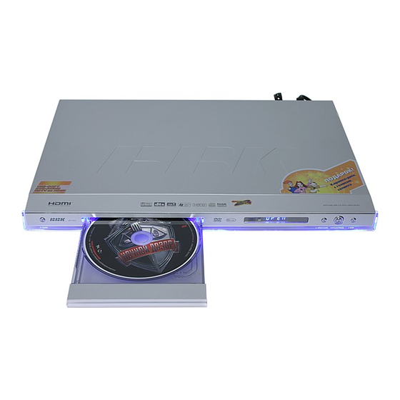
Page 9: Control Button Locations And Explanations
2.2 Control Button Locations and Explanations 2.2.1 Front Panel Illustration 9 10 Slot flap for USB IR SENSOR MIC jack Display window Headphone jack OPEN/CLOSE button POWER switch PLAY/PAUSE button Disc tray STOP button 2.2.2 Rear Panel Illustration Mixed Audio out jack Video Component /Y Pb Pr out jacks 5.1CH Audio Out jack Digital Audio Coaxial Out jack... -
Page 10: Accessories
ETUP Button Function Setup. Button Open/close the virtual keyboard function. KARAOKE Button Karaoke operation menu. Button Fast backward play. Button Skip backward. PEPEAT Button Repeat play. A-B Button Repeat the select. Button Press once to stand by, Press twice to play. SUBT Button Change subtitle language. -
Page 11: Language
1.Press the [SETUP] button and the screen Setup menu Russian displays the selection menu of function setup. DVD menu English Soundtrack Ukrainian Sbutitles Language Setup menu Image DVD menu 1.Setup menu: This item is used to set the Sound Soundtrack prompts language on the screen. -
Page 12: Sound
4.TV format: To set the aspect ratio of this #Optional setting: L+R, L, R. player’s output image. #Default: L+R. #Optional setting: 4:3 Pan-scan, 16:9 letterb., C.Surr. Mix: To set output means of the surround 16:9 TV, Wide/SQZ. left and right audio when playing a stereo disc. #Default: 16:9 TV. -
Page 13: Playback
G. PRO Logic II: To set PRO Logic II to ON or skipped to play the movie directly. OFF. If the TITLE does not support this Advertisemenu function, we recommend that you set this item #Optional setting: Yes, NO to AUTO because it would become worse if the #Default: Number processing effects were added forcibly. -
Page 14: Preference
#Default: 7890. Microphone Kar. help No ast. Volume Old password Echo New password 2.4.7 Preference Verify Cancel Backlight Gr. equalizer 2.4.9 Initial setup Screen saver 1.Backlight:This item is used set color of led on Auto the front panel. NTSC #Optional setting: On, Off. Press [UP/DOWN] arrow to select the #Default: On. - Page 15 DVD-Video, Super VCD, VCD, DivX 3.11, DivX 4,DivX 5, Divx Pro, XviD, CD-DA, Playerable discs CD+G, DVD-Audio,HDCD, MP3, WMA, Kodak Pictur e CD, JPEG MIC input Inputs Analog audio output: Stereo, output 5.1CH Outputs Audio outputs Digital audio output: Coaxial,Opcical Composite, S-Video, component Y Cb Cr, progressive scan Video outputs output Y Pb Pr, RGB/SCART...
- Page 16 Power cons umption Dimensi ons: 380mm 258mm 41.5mm General Spec ificat ions Mass: Operating Temperature 5~35 Operating Humi dity 15~75%(no c ondensation) #Design and specifications are subject to change without notice. #We so not guarantee that all discs can be played smoothly due to the disc quality, disc recording quality and recording format.
-
Page 17: Chapter Three Principle And Servicing
Chapter Three Principle and Servicing Section One Principle of the Player 3.1.1 Functions and features This player adopts new generation DVD decode chip, with built-in Dolby decoder, which creates vivid surround sound effect to bring you to taste cinema effect. It has the following features: Progressive scanning output produces steadier and clearer pictures with flickering. - Page 18 Earphone SDRAM 64M CS5340 FLASH16M Panel U214 U211 U203 Audio VR-DVD amplifying CD/DVD audio VR-CD Switch U209 U210 VR-DVD LDO2 Laser power U211 VR-CD LDO1 control ASPDIF Loader YUV1 DVD:A/B/C/D/RFO YUV2 CD:A/B/C/D/E/F YUV3 Video CVBS filtering YUV4 clamping TRIN YUV5 TROUT YUV6 LIMIT...
-
Page 19: Introduction To Ic Of The Player
3.1.3 Introduction to IC of the player Introduction to IC of the player is shown as in the following table: PCB semi-finished IC model Location Function product name MT1389HD U201 Decode chip 24C02 U202 EEPROM CS5340 U203 HCU04 U205 Phase inverter Decode board FLA SH U207... -
Page 20: Section Two Unit Circuit Principle
Section Two Unit Circuit Principle 3.2.1 Introduction to laser head 1. Function introduction to laser head flat cable is shown as the following table: Signal flow Name DVD disc CD disc No disc Function description direction Input loader 2.52 2.34 0.46 Focus error signal is added to two sides of pick-up focus coil... -
Page 21: Servo Circuit
Blanking unused 0.01 LD-DVD Input loader 2.21 DVD laser power control signal unused 0.01 0.01 Grounding Note: 1. When reading DVD, there are only A, B, C, D signals. 2. When reading CD, there are A, B, C, D, E, F signals. 3. - Page 22 Switch circuit MD11 LDO2 APC circuit LDO2 A B C D E F RFO XS101 FOSO FMSO MT1389 TRSO DMSO Feed electric AM5888 machine Main axis electric Open/close machine circuit Main axis control detect circuit Figure 3.2.2.1 Servo circuit block diagram 2.
-
Page 23: Cd/Dvd Conversion Circuit
equalization Frequency compensation inside MT1389, another part of signals are changed into digital signals through internal A/D converter. When loader is reading CD/VCD signals, these signals are conducted EFM demodulation inside MT1389, and then outputted to latter stage for AV decoding after finishing CIRC (Cross-Interleaved Reed-Solomon Code) error correction inside. -
Page 24: Laser Power Control Circuit
2. Working principle After loading disc in the player, IOA port of MT1389 is defaulted high level to make Q305 saturation on and form loop together with CD laser power control circuit on CD. At the same time, IOA also goes to loader PD IC to switch, disc begins to rotate, when servo management system recognizes that the disc in player is not CD disc, IQA pin outputs low level to make Q305 cut off and make Q303 on, and form loop together with DVD laser power control circuit on loader to perform disc reading acts. -
Page 25: Open/Close Door Drive Circuit
When reading VCD disc, laser power becomes weak, voltage of MDII pin decreases, voltage decrease of pin 23 of MT1389 makes voltage of pin 19 of XS301 increase to reach the purpose of raising laser power. When laser power is too strong, voltage of MDII pin increases to lead to voltage of pin 23 of MT1389 increase to make voltage of pin 19 of XS301 decrease to reach the purpose of reducing laser power to form an auto power control circuit. -
Page 26: Main Axis Control Circuit
3. Key point voltage (unit: V) is shown as the following table: Q306 Q307 State Base electrode B Collector C Em ittor E Base electrode B Collector C Em ittor E Read disc 5.06 5.06 5.01 5.03 5.06 Open disc tray to 4.79 4.77 5.06... - Page 27 2. Function: disc is always in high speed rotation in the course of disc reading, when you need to open the door to change disc, MT1389 stops the positive direction drive signal which is given to main axis drive circuit, for the function of inertia disc is still rotating. If disc out order is performed at this time, disc will be abrasively damaged.
-
Page 28: Decode Circuit
3.2.7 Decode circuit 1. Decode circuit block diagram is shown as in the following figure 3.2.7.1: SDCLK SDCKE DRAS MT 1389 A0~A20 SDRAM FLASH DQM0 AD0~AD7 DQM1 DQ0~DQ15 URST MA0~MA11 1.8V Reset EEPROM Clock voltage circuit regulating 24C02 U206 Figure 3.2.7.1 Decode circuit block diagram 2. -
Page 29: Video Circuit
User information storage: information content set by user is saved inside EEPROM, if user does not refresh or reset this information, it will saved in IC permanently. Audio, video output circuit: at present, MT1389 all integrates video D/A converter, MT1389E inside integrates audio D/A converter, manufactures select according to their own needs. -
Page 30: Reset Circuit
3.2.9 Reset circuit 1. Reset circuit is shown in the figure 3.2.9.1: DV33 R221 URST# R222 TC208 47uF/10V R220 C272 1N4148 R219 Q201 D201 2SC1815-YS Figure 3.2.9.1 Reset circuit diagram 2. Working principle: after power on, voltage of DV33 increases to 3.3V, main chip power supply is normal, because voltage of DV33 cannot change suddenly, Q201 base electrode has current in, Q201 is saturated on, URST is low level;... -
Page 31: Mute Circuit
2. Working principle: MT1389 has built-in DAC conversion circuit, which stimulates audio signals to output from decode chip directly, through audio amplifying and filtering circuit, directly output audio signals to audio terminal. Another path of L/R signal outputs to headphone circuit of MIC board for processing and then output from headphone. -
Page 32: Power Circuit
3. Working principle of power-off quieting: Shown in the figure 3.2.11.1, when the player is working normally, D204 is on, +5V charges capacitor Tc235 through D204, now voltage of Q214 emitter electrode is lower than that of base electrode, Q214 cuts off. When power off, +5V disappears, base electrode of Q214 changes to low level, And the emitter electrode changes to high level due to discharge of TC235, now Q214 is on, Q214 collector electrode (AMUTE) outputs high level to add to base electrode of switch pipe Q 205 - Q210,... -
Page 33: Usb Jack Circuit
(2) Bridge rectification and filtering circuit: the function of this circuit is to converse electric supply into DC power, the voltage after being rectified and filtered is 1.414 times of input power, so the DC voltage at the two ends of TC501 is about equal to 300V (3) Absorption loop: for power is always working in on/off state and will produce very high peak voltage, in order to well protect switch IC, a peak absorption loop is added. -
Page 34: Av Output Board Circuit
3.1.14 AV output board circuit 1. AV output board is mainly composed of audio/video output terminal, SCART output terminal, mode switch circuit and filtering circuit. output board outputs different signals to connect with the corresponding external equipment. AV output board circuit block diagram is shown as in the following figure 3.1.14.1: RGB_CVBS... -
Page 35: Panel Control Circuit
(3) SCART terminal function selection is shown as the following table: PDATO PDAT1 PDAT2 Pi n 8 of SCART termi n al Function × AV4:3 × 7.5V AV16:9 × 0.90V × 0.85V × × × CVBS MODE × × × RGB MODE Note: PDAT0 and PDAT2 are used to control input voltage of pin 8 of SCART terminal;... -
Page 36: Hdmi Circuit
3.2.16 HDMI circuit 1. HDMI circuit block diagram is shown in the figure 3.2.16.1, “Source” refers to device with HDMI output jack and “Sink” refers to device with HDMI input. HOUSE Source HDMI Sink Video TMDS Chnanel 0 Video TMDS Chnanel 1 Audio Audio TMDS Chnanel 2... - Page 37 I2C bus from pin 101, 102 of 1389B to pin 21, 22 of 1392E. Line synchronous signal HSYNC# and filed synchronous signal VSYNC# outputted by 1389 from 179, 181 are sent to pin 38, 39 of 1392E. Pin 110 of 1389 outputs signal to send to pin 27 of 1392E to fulfill the control to 1392E.
-
Page 38: Section Three Servicing Cases
Section Three Servicing Cases 3.3.1 Servicing cases Example 1 Symptom: power not on Description: insert power plug, standby indicator light is not on and the player cannot be switched Analysis and troubleshooting: test power board 5V, 3.3V voltage and they are normal; check decode board 1389 chip power supply and they are 3.3V and 1.8V, which is normal;... - Page 39 Output; check decode board U203 OKR, OKL and there is signal input; test U210 power supply 3.3V and it is normal; use oscillograph to test three data clock of SACLK, SBCLK, SLRCK that 1389 chip outputs to U210 and they are normal, so we doubt that the trouble may be caused by U203 or rosin joint; weld U203 again , test and trouble is removed.
- Page 40 Value on two ends of nerve line and nerve line jack is large; change nerve line jack XS301 and trouble is removed. Example 10 Symptom: not read disc Description: not read any discs Analysis and troubleshooting: not read any discs, observe laser head action carefully and find there is no focus action;...
- Page 41 output and there is 2.45V voltage; check each signal output pin of U209 and there is 2.5V voltage; check two ends of Tc240 capacitor and there are 2.5V voltage; power off and test Tc240 capacitor and there is 200-ohm resistance; after changing this capacitor, trouble is removed. Example 15 Symptom: HDMI has no output Description: other video channel output is normal, only HDMI port has no output Analysis and troubleshooting: when this trouble appears, check pin 18 of HDMI output terminal,...
-
Page 42: Troubleshooting Flow Chart
3.3.2 Troubleshooting flow chart 1. Troubleshooting process for “power not on” is shown in the figure 3.3.2.1: Power not on for the player Whether power board +5V Check according to troubleshooting power supply is process for “Power board not on” normal Whether Whether... - Page 43 2. Troubleshooting process for “Video has no output” is shown in the figure 3.2.2.2: Video has no output Check whether output Restore setup mode mode switch is correct Check Check whether power whether 27M clock is supply of MT1389 video Restore setup mode normal output part is...
- Page 44 3. Troubleshooting process for “No sound output” is shown in the figure 3.2.2.3: No sound output Whether +9V, -9V power supply Check power supply circuit is normal Whether decode chip has audio Check decode chip signal output Whether Q213 collector electrode Check mute circuit is low level Check according to troubleshooting...
- Page 45 4. Troubleshooting process for “Left channel has no sound” is shown in the figure 3.2.2.4: Left channel has no sound Check whether pin 226 of MT1389 has trouble MT1389 has sound output Check whether pin 2 of Check the line between U209 has audio signal MT1389 and U209 input...
- Page 46 5. Troubleshooting process for “Power not on” is shown in he figure 3.2.2.5: Power not on Whether Whether Check fuse tube and two ends of TC501 two ends of power power cord have 300V grid filter have AC voltage input Check rectifying tube D501 D504 Whether...
- Page 47 6. Troubleshooting process for “Not read disc” is shown in the figure 3.2.2.6: Not read disc Check Whether Check whether disc in/feed to whether loader has pin 26 of AM5888S proper position detect circuit reset when no has feed signal and MT1389 are normal disc in input...
- Page 48 Check Check whether MT1389 and whether LDO_DV33 is R201, C210 is normal normal Check whether LD01 is Check MT1389 normal Change 24P flat cable cord Load disc and observe Whether Change loader whether disc rotation there is RF signal speed is normal Change Whether...
-
Page 49: Section Four Waveform Diagram
Section Four Waveform diagram This section collects signal waveform diagram of audio, video and each unit circuit with the purpose to help servicing personnel to judge where trouble lies in accurately and quickly to improve servicing skills. For the difference of oscillograph's type, model and tuner, a certain difference may exist, so the servicing personnel are expected to pay more attention to check in daily operation. - Page 50 3. A signal waveform diagram of pin 15 of XS301(B C D E F 4. DMO signal (when there is main axis rotation) waveform diagram of pin 37 of U201 (Mt1389) 5. FMO signal (when there is feed) waveform diagram of pin 38 of U201 (MT1389) - 46 -...
- Page 51 6. TRO signal (when there is trace) waveform diagram of pin 41 of U201 (MT1389) 7. FOO signal (when there is focus) waveform diagram of pin 42 of U201 (MT1389) 8. Waveform diagram of pin 29 (when no disc in) of U207(FLASH) - 47 -...
- Page 52 9. Waveform diagram of pin 38of U208 (SDRAM) 10. Video signal waveform diagram 11. ACLK (12.2878MHZ): waveform diagram for external clock signal - 48 -...
- Page 53 12. ABCK (3.07195MHZ): waveform diagram for bit clock signal 13. ALRCK (48KHZ): waveform diagram for left/right channel clock signal 14. SDATA0: waveform diagram for mixed left/right channel digital signal - 49 -...
- Page 54 15. SDATA1: waveform diagram for surround left/right channel digital signal (now the disc being played is 2.1CH, and this signal has no output; if 5.1CH, the form is the same with that of SDATA0) 16. SDATA2: waveform diagram for centre subwoofer digital signal 17.
- Page 55 18. LEF#: waveform diagram for subwoofer channel analog signal 19. AMDAT: waveform diagram for microphone signal after 5340 A/D conversion 20. SPDIF: waveform diagram for optical/coaxial digital audio signal - 51 -...
- Page 56 21. 27M clock signal waveform diagram 22. Reset circuit waveform diagram URST# Dv33 - 52 -...
-
Page 57: Section Five Function Introduction To Ic
Section Five Function Introduction to IC 3.5.1 Function introduction to MT1389HD 1. Description MT1389HD (U201) is a cost-effective DVD system-on-chip (SOC) which incorporates advanced features like MPEG-4 video decoder, high quality TV encoder and state-of-art de-interlace processing. Based on MediaTek’ s world-leading DVD player SOC architecture, the MT1389E is the 3rd generation of the DVD player SOC. - Page 58 (2)High Performance A nalog RF Amplifier Programmable fc Dual automatic laser power control Defect and blank detection RF level signal generator (3)Speed Performance on Servo/Channel Decoding DVD-ROM up to 4XS CD-ROM up to 24XS (4)Channel Data Processor Digital data slicer for small jitter capability Built-in high performance data PLL for channel data demodulation EFM/EFM+ data demodulation Enhanced channel data frame sync protection &...
- Page 59 Provides the self-refresh mode SDRAM Block-based sector addressing (9)Video Decode Decodes MPEG1 video and MPEG2 main level, m ain profile video (720/480 and 720x576)Decodes MPEG-4 Advanced Simple Profile Support DivX 3.11/4.x/5.x Home Theater Profile Support Nero-Digital Smooth digest view function with I, P and B picture decoding Baseline, extended-sequential and progressive JPEG image decoding Support CD-G titles (10)Video/OSD/SPU/HLI Processor...
- Page 60 (12)TV Encoder Four 108MHz/12bit DACs Support NTSC, PAL-BDGHINM, PAL-60 Support 525p, 625p progressive TV format Automatically turn off unconnected channels Support PC monitor (VGA) Support Macrovision 7.1 L1, Macrovision 525P and 625P CGMS-A/WSS Closed Caption (13)Progressive Scan Video Automatic detect film or video source 3:2 pull down source detection Advanced Motion adaptive de-interlace Minimum external memory requirement...
- Page 61 DVDRFIN Analog input AC coupled DVD RF signal input RFIN Analog input DC coupled main beam RF signal input A Analog input DC coupled main beam RF signal input B Analog input DC coupled main beam RF signal input C Analog input DC coupled main beam RF signal input D Analog input...
- Page 62 Negative main beam summing output SGND Ground Analog ground Analog output Focus error monitor output Analog output Tracking error monitor output TEZISLV Analog output TE slicing Level Analog monitor output (6) RFVDD3 Analog output Analog Power RFRPDC Analog Input RF ripple detect output RFRPAC Analog output RF ripple detect input(through AC-coupling)
- Page 63 Focus servo output. PDM output of focus servo Analog output compensator LVTTL3.3 Input, Monitor hall sensor input ADIN1 Schmitt input, pull up, AD input 1 (Digital pin) GPIO with analog input path GPIO for ADIN1 General Power/Ground (18) DVDD18 Power 1.8V power pin for internal digital circuitry DVSS Ground...
- Page 64 InOut 4~16mA,SRPU Microcontroller address/data 6 InOut 4~16mA,SRPU Microcontroller address/data 5 InOut 4~16mA,SRPU Microcontroller address/data 4 InOut 4~16mA,SRPU Microcontroller address/data 3 InOut 4~16mA,SRPU Microcontroller address/data 2 InOut 4~16mA,SRPU Microcontroller address/data 1 InOut 4~16mA,SRPU Microcontroller address/data 0 IOA 0 InOut 4~16mA,SRPU Microcontroller address IOA 1 InOut 4~16mA,SRPU Microcontroller address 1/ IO...
- Page 65 InOut 4~16mA, UWR# Microcontroller write strobe, active low SRPD,SMT InOut 4mA, URD# Microcontroller read strobe, active low SRPD,SMT InOut 4~16mA, UP1_2 Microcontroller port 1-2 SRPD,SMT InOut 4mA, UP1_3 Microcontroller port 1-3 SRPD,SMT InOut 4mA, UP1_4 Microcontroller port 1-4 SRPD,SMT InOut 4mA, UP1_5 Microcontroller port 1-5 SRPD,SMT...
- Page 66 I) Serial interface port 0 data-in II) GPIO 1) Audio left/right channel clock of SPDIF input SPLRCK SDO0 Inout 2) While SPDIF input is not used: I) Serial interface port 0 data-out II) GPIO 1) Audio bit clock of SPDIF input SDCS0 2) While SPDIF input is not used: SPBCK...
- Page 67 4) While using external channels: I) GPO_1 1) Audio serial data 2 (Center/LFE) 2) DSD data right surround channel 3) Trap value in power-on reset: InOut 4mA, ASDATA3 I) 1: manufactory test mode PD,SMT II) 0: normal operation 4) While only 2 channels output: I) GPO_0 1) Audio serial data 3 (Center-back/ Center-left-back/Center-right-back, in 6.1 or 7.1 mode)
- Page 68 b. GPIO AVCM Analog AUDIO DAC reference voltage 1) AUDIO DAC Left Surround channel output 2) While internal AUDIO DAC not used: GPIO Output a. SDATA2 b. GPIO 1) AUDIO DAC Left Surround channel output 2) While internal AUDIO DAC not used: GPIO Output a.SDATA0...
- Page 69 Output 1) Video data output bit 6 YUV 6 R/Cr/Pr 4MA, SR 2) Red or CR 1) Vertical sync input/output 2) While no External TV-encoder: Output VSYN V_ADIN1 I) Vertical sync for video-input 4MA, SR II) Version AD input port 1 III) GPIO 1) Video data output bit 7 2) While no External TV-encoder:...
- Page 70 MISC (12) InOut PRST# Power on reset input, active low PD,SMT InOut PD,SMT Microcontroller ICE mode enable XTALO Output 27MHz crystal output XTALI Input 27MHz crystal input USB_VSS USB Ground USB ground pin USBP Analog Inout USB port DPLUS analog pin USBM Analog Inout USB port DMINUS analog pin...
- Page 71 IO_9(RD2 1) Digital Video output Y bit 0 InOut Non-pull 2) GPIO IO_10(RD 1) Digital Video output Y bit 1 InOut Non-pull 2) GPIO IO_11(RD 1) Digital Video output Y bit 2 InOut Non-pull 2) GPIO IO_12(RD 1) Digital Video output Y bit 3 InOut Non-pull 2) GPIO IO_13(RD...
- Page 72 RWE# output DRAM Write enable, active low DQM1 InOut Data mask 1 IO_18 (DQS1) InOut Non-pull GIPIO InOut DRAM data 8 InOut DRAM data 9 RD10 InOut DRAM data 10 RD11 InOut DRAM data 11 RD12 InOut DRAM data 12 RD13 InOut DRAM data 13...
-
Page 73: Function Introduction To At24C02
3.5.2 function introduction to AT24C02 1. Description The AT24C02 (U202) provides 2048 bits of serial electrically erasable and programmable read-only memory (EEPROM) organized as 256 words of 8 bits each. The device is optimized for use in many industrial and commercial applications where low-power and low-voltage operation are essential. The AT24C02 is available in space-saving 8-lead PDIP, 8-lead MAP, 8 lead TSSOP and 8-ball dBGA2 packages and is accessed via a 2-wire serial interface. -
Page 74: Function Introduction To Cs5340
Serial SCL input TEST Test port Positive Power Supply 3.5.3 function introduction to CS5340 1. DESCRIPTION The CS5340 (U203) is complete analog-to-digital converter for digital audio systems. It performs sampling, analog-to-digital conversion and anti-alias iltering, generating 24-bit values for both left and right inputs in serial form at sample rates up to 200 kHz per channel. -
Page 75: Function Introduction To 74Hcu04
LRCK Left right clock /RST Reset AINL Analog input L Quiescent voltage AINR Analog input R Analog power REF_GND FILT+ Positive voltage reference Mode selection 1 3.5.4 function introduction to 74HCU04 1. Description The 74HCU04 (U205) is a high-speed Si-gate CMOS device and is pin compatible with low power Schottky TTL (LSTTL). -
Page 76: Function Introduction To Sdram
1-9、16-25、48 AO-A19 20 bit address bus Write enable signal, low level is effective 3.23V RESET Reset, low level is effective 3.23V 10、13、14 Blank pin RY/BY Ready/system busy 3.23V Chip enable, low level effective 27、46 Ground Output enable signal , low level is effective ... -
Page 77: Function Introduction To 4580
VDDQ 3.3V power supply Blank Data bus Clock enable signal Data bus System clock input Data input/output VSSQ Ground UDQM screen-shielded signal Data bus Blank 3.3V power supply Ground Data input/output screen-shielded LDQM Data bus signal ... -
Page 78: Function Introduction To D5954
2. FEATURES ◆ Operating Voltage ( ±2V~±18V ) ◆ Low Input Noise Voltage ( 0.8µVrms typ. ) ◆ Wide Gain Bandwidth Product ( 15MHz typ. ) ◆ Low Distortion ( 0.0005% typ. ) ◆ Slew Rate ( 5V/µs typ. ) ◆... -
Page 79: Function Introduction To Pt6961
VOSL External feedback resistor VINFFC Focus feedback signal input 5V power supply PVCC1 5V power supply PGND Ground VOSL- Main axis drive reverse voltage output VO2+ Main axis drive forward direction voltage output VOFC- Focus drive reverse voltage output VOSC+ Focus drive forward voltage output VOTK+ Trace drive forward direction voltage output... - Page 80 ◆ Multiple Display Modes (12 segment, 6 Grid to 11 segment, 7 Grid) ◆ Key Scanning (10 x 3 Matrix) ◆ 8-Step Dimming Circuitry ◆ Serial Interface for Clock, Data Input, Data Output, Strobe Pins ◆ Available in 32-pin, SOP Package 3.
-
Page 81: Function Introduction To Viper22Adip
Grid output Grid output Ground Grid output Grid output Ground 3.5.10 function introduction to VIPer22ADIP 1. DESCRIPTION The VIPer22A (U501) combines a dedicated current mode PWM controller with a high voltage Power MOSFET on the same silicon chip. Typical applications cover off line power supplies for battery charger adapters, standby power supplies for TV or monitors, auxiliary supplies for motor control, etc. -
Page 82: Function Introduction To P H817
DRAIN Power MOSFET drain. DRAIN Power MOSFET drain. DRAIN Power MOSFET drain. 3.5.11 Function introduction to PH817 PH817 (U502) is a photoelectric coupler, shown as the figure 3.5.11.1. The right side is a light emitting diode, which sends out light of different intensity according to the strength of voltage inputted from the right side, generates photocurrent of different intensity on the left side according to light of different intensity, and outputs from position D. -
Page 83: Function Introduction To 455 8
3.5.13 Function introduction to 4558 1. Description The RC4558 and RM4558 devices (U601) are dual general-purpose operational amplifiers with each half electrically similar to the A741 except that offset null capability is not provided. The high common-mode input voltage range and the absence of latch-up make these amplifiers ideal for voltage-follower applications. -
Page 84: Function Introduction To Tda1308
3.5.14 Function introduction to TDA1308 1. DESCRIPTION The TDA1308 (U603) is an integrated class AB stereo headphone driver contained in an SO8, DIP8 or a TSSOP8 plastic package. The device is fabricated in a 1 mmCMOS process and has been primarily developed for portable digital audio applications. -
Page 85: Function Introduction To Mt1392E
3.5.15 Function introduction to MT1392E 1. Description MediaTek MT1392E (U701) is a multi-resolution HDMI transmit processor, which incorporates video scaler, high definition TV encoder, audio sampling rate converter, audio packer, HDCP processor and HDMI transmItter. This IC can accept digital video in various definition, including standard-definition video such as 480i, 576i, 480p, 576p, and high-definition video such as 720p (50/59.94Hz), 1080i(5059.94Hz), and converts the standard definition video into high-definition ones. - Page 86 Normal : Digital chroma input C0-C7 I,PD VDAC test DAC test mode [0:7] input. BIST mode : BIST data input DVDD33 Digital power, 3.3V Clock of digital video input DVSS Digital ground Normal : Digital luma input 13-20 Y0-Y7 I, PD VDAC test : DAC test data [0:7] input.
- Page 87 MSCK/GPO5 BIST mode : SRAM fail output Normal : General purpose output MasterI2C on : Master serial interface data input output MSD/GPO6 IO,PU BIST mode : SRAM fail output Normal : General purpose output GPO7 IO,PD Power ON : EPROM word-address type 1 : 16bit , 0 : 8bit BIST mode : SRAM fail output Normal : General purpose output BIST mode : SRAM fail Output...
- Page 88 AVSS Analog Ground SWING HDMI output swing adjustment AVDD Power of DAC, 3.3V VREF Voltage reference of DAC DAC full scale adjustment AVSS Ground of DAC AVDD Power of DAC, 3.3V AVSS Ground of DAC AVDD Power of DAC, 3.3V Component analog video output Y/Green AVSS Ground of DAC...
-
Page 89: Chapter Four Disassembly And Assembly Process
Chapter Four Disassembly and Assembly Process DVD players manufactured in BBK are largely identical but with minor differences and are mainly composed of loader components, control panel components, decode and servo board components, power board components, power amplifier board components, MIC board components and AV board components. -
Page 90: Chapter Cinque Pcb Board & Circuit Diagram
Chapter Cinque PCB board & Circuit diagram Section One PCB board 5.1.1 Surface layer of KEY SCAN Board VD406 VD402 VD403 TC402 VD404 K405 K403 K402 U402 LED401 TC401 4DV985-1 LEI DVD 2006/03/22 - 86 -... - Page 91 5.1.2 Bottom layer of KEY SCAN Board R405 C403 L401 XS401 R420 D412 D408 C401 R412 C408 D407 R409 D405 D414 D402 R415 R408 R411 C402 R402 Q404 D403 U401 D404 D401 R403 R407 R401 R404 - 87 -...
- Page 92 5.1.3 Surface layer of DECODE&SERVO Board - 88 -...
- Page 93 5.1.4 Bottom layer of DECODE&SERVO Board - 89 -...
- Page 94 5.1.5 Surface layer of HDMI Board JK708 R749 XS704 R745 R744 R756 XS703 R703 R704 R705 C751 U701 L718 L719 XS701 R726 R718 R743 - 90 -...
- Page 95 5.1.6 Bottom layer of HDMI Board C739 C737 C738 C753 C745 - 91 -...
- Page 96 5.1.7 Surface layer of MIC Board L606 TC605 JP604 JP606 JP602 TC601 6DV718-1 TC614 2006/6/28 R629 TC607 TC620 TC617 TC618 JP605 R621 TC615 JK602 U601 JP601 TC616 R622 TC619 JP603 JP607 G601 JP608 G602 JP609 L605 JP610 MIC601 JK601 - 92 -...
- Page 97 5.1.8 Bottom layer of MIC Board R603 R623 U603 R625 R608 R630 L601 R601 C611 R628 C604 R627 C606 R610 C623 C609 Q601 R604 R607 R632 R631 C603 R633 R606 C602 C616 R605 R613 C601 C624 C625 R639 R640 R641 R624 - 93 -...
- Page 98 5.1.9 Surface layer of AV Board JP702 JP716 JK705 JK702 JK706 R708 V702 R709 JP715 V703 JP719 JP709 R711 JP705 V701 L714 L715 R712 7DV718-0 JP710 XS702 JP706 L713 DVD 2006/06/17 JP707 XS701 XS703 - 94 -...
- Page 99 5.1.10 Bottom layer of AV Board R701 C710 C711 C716 C728 C726 C725 ZD704 R703 ZD703 ZD702 ZD701 C727 R704 D703 R714 R710 D704 D705 C723 C706 R705 C724 L703 R706 C705 R719 L702 C703 L701 R718 C701 R717 - 95 -...
-
Page 100: Power Board
5.1.11 POWER Board D512 CAUTION: FOR CONTIUED PROTECTION HIGH G502 TC508 G504 D507 D509 AGAINST RISK OF FIRE REPLACE ONLY U504 F501 WITH SAME TYPE VOLTAGE D513 T1.6A L250V FUSE BC505 T501 TC504 BCN502 BCN501 ~220V ~220V C508 CN502 TC501 R510 D504 ZD501... - Page 101 UPD[15..0] U207 UPA[20..0] 1*16MBit_FLASH(TSOP) L208 DV33 BYTE FBSMT DQ15/A-1 C279 TC219 DQ14 47uF/10V MA10 DQ10 A10/AP DQ10 MA11 DQ11 DQ11 DQ13 DBA0 DQ12 R234 BA0/A13 DQ12 DBA1 DQ13 AA21 R235 BA1/A12 DQ13 A20/NC DQ12 DQ14 PWR# DQ14 DCLK R236 SDCLK DQ15 DQ15 RESET...
- Page 102 AVCC V1P4 R294 0R JITFO C219 JITFN 89_VSYNC## 89_VSYNC# DV33 C223 APLLVDD3 L203 4.7uH R308 R309 RFVDD3 89V33 DV33 PLLVDD3 R295 20pF SCART 100K R211 C224 ADACVDD L204 22uH R209 C237 C238 C239 C229 2N3904 R303 Q305 TC203 750K R311 C240 TC204 DVD: 0V...
- Page 103 R2111 30K R227 MIC_DET C2111 L209 FBSMT +A9V R2117 R2123 XS206 R2135 4.7K TC246 89_AR R2160 CH-R USBP TC240 C2117 10uF/16V USBM R2136 10uF/16V -A9V U209B R2147 4580 100K Q205 R285 AGND R2112 30K 2SC1815-YS MUTE-1 OKA# R2137 AGND C2112 DV33 DV33 R2148...
- Page 104 89_HSYNC# R223 89_VSYNC# IEC958 DV33 YUV6 YUV4 YUV4 LFE# R228 YUV5 5.1K YUV6 YUV5 SPDATA XS204 XS17 R224 C270 ASPDIF ASDAT3# ASDAT1# AGND ASDAT2# VIDEO# R213 0R(NC) ASDAT0# R292 SACLK R214 0R(NC) SBCLK LFE# R293 SLRCK JK701 AV8-2 XS207 L205 XS45 0402 PIN1-14...
- Page 105 D401 D402 open/close 1N4148 XS402 K403 step LED01 1N4148 VCC1 play/pause KEY1 KEY2 XS04/2.0 K402 K405 KEY3 U402 VCC1 HS0038B3V U401 L401 R401 DOUT LEDAT LED401 LEDCK R405 R420 LEDST 100R KEY1 KEY2 KEY3 SEG1/KS1 C408 SEG2/KS2 SEG12/GR7 C401 SEG3/KS3 SEG11 TC402 LED-SOCK(1)
- Page 106 R622 C616 JK601 -9VA PHONEJACK TC617 TC619 R605 TC616 C602 47uF/16V R631 100uF/16V R625 47uF/16V 3.9K R633 4.3K C619 R627 Q601 R621 104(NC) 8050D +9VA R635 C621 R637 104(NC) R629 R601 22R(NC) AGND R607 3.3K TC615 C601 330R XS603 47uF/16V C605 TC601 C604...
- Page 107 L701 1.8uH YUV4 VIDEO_G/Y D703 L715 FCM 1N4148*2 R717 C701 C702 ZD705 5.1V/0.5W VGND PDAT2 VGND PDAT1 SPDIF +10V R706 R709 YUV6 330R VGND YUV4 XS701 V701 L702 VGND XS14P R714 8050 1.8uH PDAT1 YUV5 YUV5 VIDEO_B/U PDAT0 2.2K D704 VIEDO# 1N4148*2 R708...
- Page 108 1392_DACVDD3 FS_1392 L717 C744 C745 VREF_1392 DV33 1392_AVDD3 FBSMT C742 C743 TC701 C746 R724 220uF/16V 560R YUV4 R703 R704 YUV5 YUV6 HGND R705 R723 HGND 510R L716 ASPDIF HGND 1392_AVDD3 1392_DACVDD3 FBSMT ASDAT3 DVSS SWING C737 C738 C739 SDATA1 AVSS SDATA2 TX2+ TX2+...
- Page 109 D512 HER105 -21V C507 TC508 ZD501 47uF/50V 5.1V 1/2W TC504 C508 100uF/16V R503 C502 D503 R510 D502 39K/2W 103/1KV 1N4007 1N4007 4.7K(DNS) D513 HER105 D501 D504 TC501 D505 1N4007 C503 22uF/400V HER107 D507 D509 L507 10uH/2A D510 1N4007 101/1KV(DNS) HER303 +3.3V TC505 TC506...
-
Page 110: Chapter Six Bom List
Chapter six BOM List MATERIAL MATERIAL NAME SPECIFICATIONS LOCATION CODE DV718SI(RU)SILVER[1389HD] AV BOARD:(7DV718-0 DV718SI(RU) SILVER[1389HD]) 5448709 1.3/V2.0 0090001 SMD RESISTOR 1/16W 0O±5% 0603 C717,C720,C722 0090006 SMD RESISTOR 1/16W 75O±5% 0603 R717~R719,R706 0090238 SMD RESISTOR 1/16W 68O±5% 0603 R703 0090181 SMD RESISTOR 1/16W 100O±5% 0603... - Page 111 F 0.6 SHAPED 7.5mm JP701,JP704,JP710,JP717,JP718 2100004 LEAD F 0.6 SHAPED 10mm JP703 2100006 LEAD F 0.6 SHAPED 12.5mm JP702 1564359 PCB 7DV718-0 DV718SI(RU)SILVER[1389HD] DECODE BOARD:2DV718-2 1.8/Ver2.3 0090324 SMD RESISTOR 1/16W 0O±5% 0402 R213,R214,R318 0090445 SMD RESISTOR 1/16W 1O±5% 0402 R321 0090457 SMD RESISTOR 1/16W2.2O±5% 0402...
- Page 112 MATERIAL MATERIAL NAME SPECIFICATIONS LOCATION CODE 0090389 SMD RESISTOR 1/16W 15K±5% 0402 R202,R211 0090391 SMD RESISTOR 1/16W 20K±5% 0402 R325 0090394 SMD RESISTOR 1/16W 27K±5% 0402 R203,R204 0090395 SMD RESISTOR 1/16W 30K±5% 0402 R2113~R2116 0090034 SMD RESISTOR 1/16W 100K±5% 0603 R210 0090398 SMD RESISTOR 1/16W 39K±5% 0402...
- Page 113 MATERIAL MATERIAL NAME SPECIFICATIONS LOCATION CODE 0310362 SMD CAPACITOR 16V474 +80%-20% Y5V 0603 C220 0390453 SMD MAGNETIC BEADS GZ1005D221T 0402 R264,L205,L207 L202,L206,L208,L209,L218~L224,L307,L30 0390095 SMD MAGNETIC BEADS FCM1608K-221T05 8,L311,L316 0390444 SMD MAGNETIC BEADS PZ2012U121 L210,L211,L235,L315 0390452 SMD MAGNETIC BEADS PZ3216D121 L212 0390096 SMD INDUCTOR 1.8UH±10% 1608 L225~L227...
- Page 114 MEET WITH CLASP SA-001-012 BLACK IRON 1910129 TERMINAL SOCKET JK703 PIECE,SCREEN-SHIELDED 1910079 TERMINAL SOCKET AV8-8.4-6G-3 JK701 1633428 PCB 2DV718-2 DV718SI(RU)SILVER[1389HD] HIGH DEFINITION SCREEN 5448708 0090001 SMD RESISTOR 1/16W 0O±5% 0603 R726 0090005 SMD RESISTOR 1/16W 33O±5% 0603 R757 0090009 SMD RESISTOR 1/16W 330O±5% 0603...
- Page 115 JK708 45P 0.5mm SMD VERTICAL REVERSE 1940289 CABLE SOCKET XS703 MEET WITH CLASP 1940024 SOCKET 5P 2.0mm XS701,XS704 1633343 PCB TDV985-1 DV718SI(RU)SILVER[1389HD] MAIN PANEL 5448083 3072182 LAMP BRACKET DV985 0620002 RADIATION DIODE F 3 RED VD406 1200788 LEDDISPLAY SCREEN 4MB40205B18...
- Page 116 0310066 SMD CAPACITOR 50V 102±10% X7R 0603 C408 SMD VOLTAGE REGULATOR 0700004 5.1V±5% 1/2W D414 DIODE 1633102 PCB 4DV985-1 DV718SI(RU)SILVER[1389HD] OK BOARD 5448710 0090009 SMD RESISTOR 1/16W 330O±5% 0603 R601 0090012 SMD RESISTOR 1/16W 560O±5% 0603 R604 0090014 SMD RESISTOR 1/16W 1K±5% 0603...
- Page 117 2100003 LEAD F 0.6 SHAPED 7.5mm JP601,JP602,JP605,JP603 1860047 USB SOCKET CAM-B85-4Pin JK602 2100004 LEAD F 0.6 SHAPED 10mm JP606 1980046 EARPHONE SOCKET ST-301-030-100 JK601 GROUND CHIP OF POWER 3870115 AB903 G601, G602 BOARD DV718SI(RU)SILVER[1389HD] POWER BOARD 5448711 - 113 -...
- Page 118 MATERIAL MATERIAL NAME SPECIFICATIONS LOCATION CODE GROUND CHIP OF POWER 3870115 AB903 G501~G504 BOARD 2300049 FUSE @T1.6AL 250V 3.6×10 VDE F501 1940045 SOCKET 2P 8.0mm 2# BCN501 1940022 SOCKET 4P 2.0mm CN501 SWITCH POWER 0460623 @BCK-19-0348 SJ T501 TRANSFORMER 1000043 POWER GRID FILTER @UT-20 40mH±20%10×13 UL L501 1080032 PHOTOELECTRIC COUPLER...
- Page 119 JP506 0210207 TERYLENE CAPACITOR @275V 104±20% 15mm VDE BC501 00700169 HIGH PRESSURE RESISTOR @1/2W680K±5% VDE BELT R501 1564443 PCB @5DV985-2 UL DV718SI(RU)SILVER[1389HD] REMOTE CONTROL 5471742 0310048 SMD CAPACITOR 50V 151±5% NPO 0603 C802,C803 0630009 EMISSION PIPE TSAL4400 LED801 0700007 SMD DIODE 1N4148 D801~D803 ⑿...
- Page 120 2B 43PC COLORLESS ISSUE BLUE 2×4× 0620203 RADIATION DIODE LED901,LED902 SMD VOLTAGE REGULATOR 0700004 5.1V±5% 1/2W D901 DIODE 1564266 PCB 9DV985-1 DV718SI(RU)SILVER[1389HD] PROGRAM FLASH ROMDV718SIRU-0A(16M) 0911767 0881650 IC 29LV160BE-70PFTN TSOP U207 ⒁ 0881651 IC M29W160EB 70N6 TSOP U207 ⒁ - 116 -...
Need help?
Do you have a question about the DV718SI and is the answer not in the manual?
Questions and answers