Table of Contents
Advertisement
UM2505
User manual
STM32G4 Nucleo-64 boards (MB1367)
Introduction
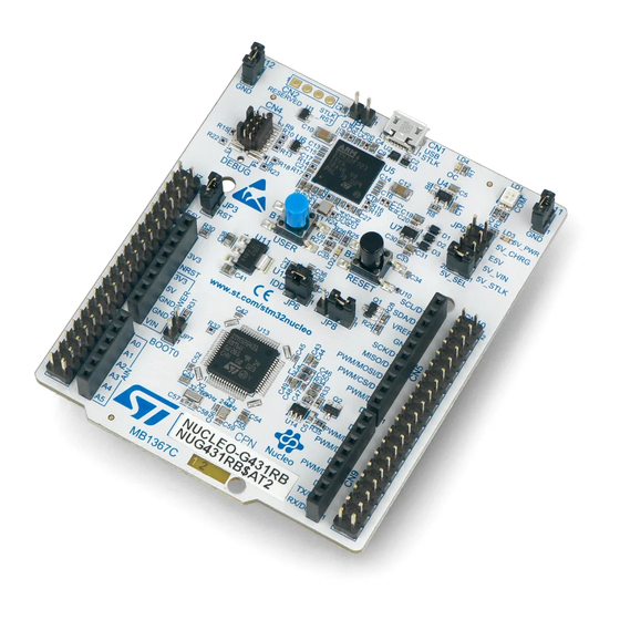
The STM32G4 Nucleo-64 boards based on the MB1367 reference board (NUCLEO-G431RB, NUCLEO-G474RE,
NUCLEO-
G491RE) provide an affordable and flexible way for users to try out new concepts and build prototypes with the STM32G4
Series microcontrollers, choosing from the various combinations of performance, power consumption and features. The
®
ARDUINO
Uno V3 connectivity and the ST morpho headers provide an easy means of expanding the functionality of the
Nucleo open development platform with a wide choice of specialized shields. The STM32G4 Nucleo-64 boards do not require
any separate probe as they integrate the STLINK-V3E debugger/programmer. The STM32G4 Nucleo-64 boards come with the
comprehensive free software libraries and examples available with the STM32CubeG4 MCU Package.
Figure 1.
NUCLEO-G474RE top view
Figure 2.
NUCLEO-G474RE bottom view
Pictures are not contractual.
UM2505 - Rev 3 - November 2020
www.st.com
For further information contact your local STMicroelectronics sales office.
Advertisement
Table of Contents

Related Manuals for ST NUCLEO-G474RE


Summary of Contents for ST NUCLEO-G474RE
-
Page 1: Figure 1. Nucleo-G474Re Top View
® ARDUINO Uno V3 connectivity and the ST morpho headers provide an easy means of expanding the functionality of the Nucleo open development platform with a wide choice of specialized shields. The STM32G4 Nucleo-64 boards do not require any separate probe as they integrate the STLINK-V3E debugger/programmer. The STM32G4 Nucleo-64 boards come with the comprehensive free software libraries and examples available with the STM32CubeG4 MCU Package. -
Page 2: Features
® – ARDUINO Uno V3 expansion connector – ST morpho extension pin headers for full access to all STM32G4 I/Os • Flexible power-supply options: ST-LINK, USB V , or external sources • On-board STLINK-V3E debugger/programmer with USB re-enumeration capability: mass storage, Virtual COM port, and debug port •... -
Page 3: Ordering Information
STM32. Table 1. List of available products Order code Board reference Target STM32 NUCLEO-G431RB STM32G431RBT6U NUCLEO-G474RE MB1367 STM32G474RET6U NUCLEO-G491RE STM32G491RET6U Codification The meaning of the codification is explained in Table Table 2. Codification explanation... -
Page 4: Development Environment
STM32 Flash memory for easy demonstration of the device peripherals in standalone mode. The latest versions of the demonstration source code and associated documentation can be downloaded from www.st.com. UM2505 - Rev 3 page 4/43... -
Page 5: Conventions
UM2505 Conventions Conventions Table 3 provides the conventions used for the ON and OFF settings in the present document. Table 3. ON/OFF convention Convention Definition Jumper JPx ON Jumper fitted Jumper JPx OFF Jumper not fitted Jumper JPx [1-2] Jumper fitted between Pin 1 and Pin 2 Solder bridge SBx ON SBx connections closed by 0 Ω... -
Page 6: Quick Start
Table 4. Jumper configuration Jumper Definition Position Comment NRST STLINK-V3E reset T_RST ON [1-2] (Default) 5V_USB_STLK (from ST-LINK) ON [3-4] (optional) 5V_VIN 5 V power-source selection ON [5-6] (optional) ON [7-8] (optional) 5V_USB_CHGR BOOT0 ON [1-2] (Default) VREF+ supplied with VREF... -
Page 7: Hardware Layout And Configuration
Figure 3 shows the connections between the STM32 and its peripherals (STLINK-V3E, push-buttons, LEDs, USB, ® ARDUINO Uno and ST morpho headers). Figure 4 Figure 5 show the location of these features on the STM32G4 Nucleo-64 board. The mechanical dimensions of the board are shown in Figure Figure 3. -
Page 8: Pcb Layout
® ® ARDUINO connector ARDUINO connector BOOT0 U14 voltage ref. IC TL1431CL5T ARDUINO ® connector ® ARDUINO connector CN10 ST morpho pin header ST morpho pin header HW102 product sticker 32 kHz 24 MHz UM2505 - Rev 3 page 8/43... -
Page 9: Figure 5. Bottom Layout
MIPI10 connector JP3 Target reset VREF selection IDD measurement ARDUINO ® connector ARDUINO ® connector JP7 BOOT0 ® ARDUINO connector ® ARDUINO connector CN10 ST morpho pin header ST morpho pin header UM2505 - Rev 3 page 9/43... -
Page 10: Mechanical Drawing
UM2505 Mechanical drawing Mechanical drawing Figure 6. STM32G4 Nucleo 64 board mechanical drawing (in millimeter) Embedded STLINK-V3E There are two different ways to program and debug the onboard STM32 MCU: • Using the embedded STLINK-V3E • Using an external debug tool connected to the CN4 MIPI10 connector. The STLINK-V3E programming and debugging tool is integrated in the STM32G4 Nucleo-64 board. -
Page 11: Drivers
STLINK-V3E product (for example new functionalities, bug fixes, support for new microcontroller families), it is recommended to visit the www.st.com website before starting to use the STM32G4 Nucleo-64 board and periodically, to stay up-to-date with the latest firmware version. -
Page 12: Using An External Debug Tool To Program And Debug The On-Board Stm32
UM2505 Embedded STLINK-V3E 6.3.3 Using an external debug tool to program and debug the on-board STM32 There are two basic ways to support an external debug tool: Keep the embedded STLINK-V3E running. Power on the STLINK-V3E at first until the COM LED turns red. Then connect the external debug tool through the CN4 STDC14/MIPI-10 debug connector Set the embedded STLINK-V3E in hig-impedance state: when jumper JP1 (STLK_RST) is ON, the embedded STLINK-V3E is in RESET state and all GPIOs are in high-impedance;... -
Page 13: Power Supply
UM2505 Power supply MIPI10 pin STDC14 pin Function Not used by SWD protocol, Target JTDI (T_JTDI) using JTAG protocol, T_JTDI only for external tools GNDDetect GND detect for plug indicator, used on SWD and JTAG neither Target NRST using SWD protocol or Target JTMS (T_JTMS) using T_NRST JTAG protocol T_VCP_RX... -
Page 14: Figure 9. Stm32G4 Nucleo-64 Board Power Tree
EN-60950-1: 2006+A11/2009 standard and must be Safety Extra Low Voltage (SELV) with limited power capability. If the power supply is 3V3, the ST-LINK is not powered and cannot be used. Power supply input from STLINK-V3E USB connector (default setting) The STM32G4 Nucleo-64 board and shield can be powered from STLINK-V3E connector CN1 (5 V) by placing a jumper between pins 1-2 of JP5, “5V_SEL”, as illustrated in... -
Page 15: Figure 10. Power Supply Input From Stlink-V3E Usb Connector With Pc (5 V, 500 Ma Max)
If an overcurrent (more than 500 mA) happens on board, the red LED LD4 is lit. The Nucleo board and its shield can be powered from ST-LINK USB connector CN1, but only ST-LINK circuit gets power before USB enumeration, because the host PC only provides 100 mA to the board at that time. -
Page 16: Table 6. External Power Sources: Vin (7 V - 12 V)
UM2505 Power supply • If the host is able to provide the required power, the enumeration finishes by a “SetConfiguration” command and then, the power switch STMPS2151STR is switched ON, the green LED LD3 (5V_PWR) is turned ON, thus Nucleo board and its shield on it can consume 500 mA at the maximum. •... -
Page 17: Table 7. External Power Sources: E5V (5 V)
UM2505 Power supply Figure 11. Power supply input from VIN (7 V - 12 V, 800 mA max) LD1117 S50TR VIN < 12 V VIN < 12 V 3.3 V Legend: Refer to Section 6.4.1 for debugging when using an external power supply. External power supply input from E5V (5 V, 500 mA max) When the STM32G4 Nucleo-64 board is power-supplied by E5V (refer to Table 7... -
Page 18: Figure 12. Power Supply Input From 5V_Ext (5 V, 500 Ma Max)
UM2505 Power supply Figure 12. Power supply input from 5V_EXT (5 V, 500 mA max) 3.3 V Legend: Refer to Section 6.4.1 for debugging when using an external power supply. External power supply input from USB charger (5 V) When the STM32G4 Nucleo-64 board is power-supplied by a USB charger on CN1 (refer to Table 8 Figure 13), the jumper configuration must be the following: jumper JP2 on pins 7-8 “5V_CHGR”. -
Page 19: Table 8. External Power Sources: 5V_Chgr (5 V)
External power sources: 5V_CHGR (5 V) Input power name Connector pins Voltage range Maximum current 5V_CHGR Figure 13. Power supply input from ST-LINK USB connector with USB charger (5 V) USB charger STLINK-V3E No debug 3.3 V Legend: UM2505 - Rev 3... -
Page 20: Table 9. External Power Sources: 3V3
When the 3.3 V is provided by a shield board, it is interesting to use the 3.3 V (CN6 pin 4 or CN7 pin 16) directly as power input (refer to Table 9 Figure 14). In this case, the programming and debugging features are not available, since the ST-LINK is not powered. Table 9. External power sources: 3V3 Input power name Connector pins... -
Page 21: Debugging While Using Vin Or Ext As An External Power Supply
Debugging while using VIN or EXT as an external power supply When powered by VIN or E5V, it is still possible to use the ST-LINK for programming or debugging only, but it is mandatory to power the board first using VIN or EXT, then to connect the USB cable to the PC. In this way the enumeration succeeds, thanks to the external power source. -
Page 22: Clock Sources
There are four ways to configure the pins corresponding to the high-speed external clock (HSE): • MCO from ST-LINK: MCO output of ST-LINK is used as input clock. This frequency cannot be changed, it is fixed at 8 MHz and connected to the PF0-OSC_IN of the STM32 microcontroller. The configuration must be: –... -
Page 23: Board Functions
The green LED indicates that the STM32G4 part is powered and +5 V power is available on CN6 pin 5 and CN7 pin 18. LD4 USB power fault (OC, overcurrent) LD4 indicates that the board power consumption on USB ST-LINK exceeds 500 mA. Consequently, the user must power the board using an external power supply. 6.6.2... -
Page 24: Current Consumption Measurement (Idd)
The STM32G4 Nucleo-64 board offers the possibility to connect an LPUART or a USART interface to the ® STLINK-V3E, ARDUINO Uno V3 connector (CN9 pins 2 and 1), or ST morpho connector (CN10 pins 35 and 37). The selection is done by setting the related solder bridges as detailed in Table 10 Table Table 10. - Page 25 PB8 not connected to ARDUINO PC5 connected to ST morpho CN10 pin 6 PC5 on ST morpho PC5 not connected to ST morpho CN10 pin 6 PB8 connected to ST morpho CN7 pin 7 PB8 on Morpho PB8 not connected to ST morpho CN7 pin 7 U12 LDO output provides 3.3 V...
- Page 26 HSE provided by external HSE 24 MHz CLK X3. & HSE not provided by external HSE 24 MHz CLK X3. SB26 PF1-OSC_IN connected to ST morpho connector I/O usage (CN7 pin 31). SB24 HSE CLK PF1-OSC_IN not connected to ST morpho connector.
- Page 27 UM2505 Solder bridges Solder Solder bridge control State Description bridge (SB) PC1 on ARD_A4 SB35 PC1 not connected to ARD_A4 and connected to CN7 pin 36. PC0 connected to ARD_A5 and connected to CN7 pin 38. PC0 on ARD_A5 SB36 PC0 not connected to ARD_A5 and connected to CN7 pin 38.
-
Page 28: Board Connectors
UM2505 Board connectors Board connectors Several connectors are implemented on the STM32G4 Nucleo-64 board. STLINK-V3E USB Micro-B connector CN1 The USB connector CN1 is used to connect the embedded STLINK-V3E to the PC for the programming and debugging purposes. Figure 15. USB Micro-B connector CN1 (front view) Table 13. -
Page 29: Arduino ® Uno V3 Connectors Cn5, Cn6, Cn8 And Cn9
UM2505 ARDUINO® Uno V3 connectors CN5, CN6, CN8 and CN9 Table 14. MIPI10 connector CN4 pinout (STDC14 pinout compatible) Connector Pin number Description Pin number Description VDD (3V3) T_SWDIO (PA13) T_SWCLK (PA14) KEY (connected to GND) T_SWO (PB3) T_JTDI (PA15) GNDDetect (connected to GND through T_NRST a 100 Ω... -
Page 30: Table 15. Arduino ® Connectors Pinout
UM2505 ARDUINO® Uno V3 connectors CN5, CN6, CN8 and CN9 ® Figure 18. ARDUINO and ST morpho connectors pinout Note: ® ARDUINO Uno V3 D0 and D1 signals are connected by default on USART1 (MCU I/O PC4 and PC5). For details about how to modify the UART interface, refer to Section 6.6.5 Virtual COM port (VCP): LPUART and... -
Page 31: St Morpho Connectors Cn7 And Cn10
ST morpho connectors CN7 and CN10 ST morpho connectors CN7 and CN10 are male pin headers accessible on both sides of the board. All signals and power pins of the STM32G4 MCU are available on the ST morpho connectors. These connectors can also be probed by an oscilloscope, logical analyzer, or voltmeter. -
Page 32: Table 16. Pin Assignment Of The St Morpho Connectors
UART interface, refer to Section 6.6.5 Virtual COM port (VCP): LPUART and USART. Table 16 shows the pin assignment of each STM32G4 I/O on the ST morpho connector. Table 16. Pin assignment of the ST morpho connectors CN7 odd pins... - Page 33 UM2505 ST morpho connectors CN7 and CN10 CN7 odd pins CN7 even pins CN10 odd pins CN10 even pins Pin nbr Pin name Pin nbr Pin nbr Pin nbr Pin name Pin name Pin name PC13 PC14 PB10 PB15 PC15...
-
Page 34: Stm32G4 Nucleo-64 I/O Assignment
UM2505 STM32G4 Nucleo-64 I/O assignment STM32G4 Nucleo-64 I/O assignment Table 17. Nucleo-64 I/O assignment Pin name Signal or label Main feature / optional feature / (SB) VBAT VBAT VBAT voltage supply PC13 PC13 USER button / IO PC14-OSC32_IN OSC32_IN / PC14 LSE CLK / IO PC15-OSC32_OUT OSC32_OUT / PC15... - Page 35 UM2505 STM32G4 Nucleo-64 I/O assignment Pin name Signal or label Main feature / optional feature / (SB) ARD_D9-TIM3_CH2 (or TIM8_CH2) / IO ARD_D7 - IO ARD_D8 - IO PA10 PA10 ARD_D2 - IO PA11 PA11 PA12 PA12 VDD voltage supply PA13 T_SWDIO T_SWDIO...
-
Page 36: Stm32G4 Nucleo-64 Board Information
Evaluation tools marked as “ES” or “E” are not yet qualified and therefore not ready to be used as reference design or in production. Any consequences deriving from such usage will not be at ST charge. In no event, ST will be liable for any customer usage of these engineering sample tools as reference designs or in production. -
Page 37: Federal Communications Commission (Fcc) And Ised Canada Compliance
UM2505 Federal Communications Commission (FCC) and ISED Canada Compliance Statements Federal Communications Commission (FCC) and ISED Canada Compliance Statements 10.1 FCC Compliance Statement Part 15.19 This device complies with Part 15 of the FCC Rules. Operation is subject to the following two conditions: (1) this device may not cause harmful interference, and (2) this device must accept any interference received, including interference that may cause undesired operation. -
Page 38: Revision History
UM2505 Revision history Table 18. Document revision history Date Version Changes 28-Mar-2019 Initial release. 17-Apr-2019 Added the Limitation section. Extended the document scope to the NUCLEO-G491RE board: updated sections Introduction, Features, Ordering information Development 26-Nov-2020 environment. Added the STM32G4 Nucleo-64 board information section. -
Page 39: Table Of Contents
UM2505 Contents Contents Features................2 Ordering information . - Page 40 ST morpho connectors CN7 and CN10 ........
-
Page 41: List Of Tables
Pin assignment of the ST morpho connectors ........ -
Page 42: List Of Figures
Figure 13. Power supply input from ST-LINK USB connector with USB charger (5 V) ......19 Figure 14. - Page 43 ST’s terms and conditions of sale in place at the time of order acknowledgement. Purchasers are solely responsible for the choice, selection, and use of ST products and ST assumes no liability for application assistance or the design of Purchasers’...
Need help?
Do you have a question about the NUCLEO-G474RE and is the answer not in the manual?
Questions and answers