
Related Manuals for Quectel M.2-FPC EVB


Summary of Contents for Quectel M.2-FPC EVB
- Page 1 M.2-FPC EVB User Guide 5G & LTE-A Module Series Version: 1.0 Date: 2023-02-17 Status: Released...
-
Page 2: Legal Notices
5G & LTE-A Module Series At Quectel, our aim is to provide timely and comprehensive services to our customers. If you require any assistance, please contact our headquarters: Quectel Wireless Solutions Co., Ltd. Building 5, Shanghai Business Park Phase III (Area B), No.1016 Tianlin Road, Minhang District, Shanghai... -
Page 3: Third-Party Rights
Except as otherwise set forth herein, nothing in this document shall be construed as conferring any rights to use any trademark, trade name or name, abbreviation, or counterfeit product thereof owned by Quectel or any third party in advertising, publicity, or other aspects. -
Page 4: Safety Information
Manufacturers of the cellular terminal should notify users and operating personnel of the following safety information by incorporating these guidelines into all manuals of the product. Otherwise, Quectel assumes no liability for customers’ failure to comply with these precautions. -
Page 5: About The Document
5G & LTE-A Module Series About the Document Revision History Version Date Author Description 2022-01-16 Fung ZHU Creation of the document 2023-02-17 Fung ZHU First official release M.2-FPC_EVB_User_Guide 4 / 41... -
Page 6: Table Of Contents
5G & LTE-A Module Series Contents Safety Information ............................3 About the Document ........................... 4 Contents ............................... 5 Table Index ..............................7 Figure Index ..............................8 Introduction ............................9 1.1. Applicable Modules ........................9 1.2. Special Mark ..........................9 Product Overview ..........................10 2.1. - Page 7 5G & LTE-A Module Series 5.4. Reset the Module ........................39 5.5. Current Consumption Test ......................39 Appendix References ........................40 M.2-FPC_EVB_User_Guide 6 / 41...
- Page 8 5G & LTE-A Module Series Table Index Table 1: Special Mark ........................... 9 Table 2: Components & Functions ......................12 Table 3: Accessories List ..........................15 Table 4: Description of Power Supply ......................16 Table 5: Description of M.2 Interface ......................18 Table 6: Description of USB Interface ......................
- Page 9 Figure 22: M.2-FPC EVB Assembly ......................34 Figure 23: Assembly of M.2-FPC EVB and the Laptop ................35 Figure 24: DIP Switches Position When the M.2-FPC EVB is Connected to Laptop ........ 36 Figure 25: M.2-FPC EVB Assembly for Testing ..................37 Figure 26: USB Ports ..........................
-
Page 10: Introduction
5G & LTE-A Module Series Introduction This user guide describes the application details of M.2-FPC EVB (evaluation board), which is an assistant tool for developers to develop applications and test basic functionalities of applicable modules. 1.1. Applicable Modules For details about the applicable modules of this EVB, see document [1]. -
Page 11: Product Overview
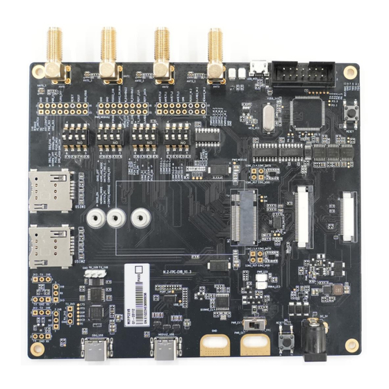
LTE-A & 5G Module Series Product Overview 2.1. Top View The size of M.2-FPC EVB is 120 mm × 135.2 mm, and the top view is shown as below: Figure 1: Top View M.2-FPC_EVB_User_Guide 10 / 41... -
Page 12: Component Placement
LTE-A & 5G Module Series 2.2. Component Placement J1308 J0901 J1302 J1304 J1306 J0902 J1201 J1203 J1202 U0902 15 1 S0901 S0302 S1101 S0401 S1102 J1001 M.2 Module J1002 J0702 D0204 D0203 S0201 S0301 H0201 U0702 U0502 J0101 135.20 mm Figure 2: Top View for Component Placement M.2-FPC_EVB_User_Guide 11 / 41... - Page 13 LTE-A & 5G Module Series Table 2: Components & Functions Components RefDes. Description Implementation Power jack on the EVB, J0101 external power supply Typical supply voltage: +5 V interface Power Supply External power supply H0201 interface for current Typical supply voltage: +3.3 V consumption test Select the module’s power Select power supply interface between...
- Page 14 LTE-A & 5G Module Series J0401, FPC Interfaces FPC connector Used to connect the laptop and the EVB J0402 S0401, S1102, Used to switch functions in different DIP Switches DIP switch S0302, modes S1101 U0902 J0901 MCU USB interface J0902 MCU JTAG interface J1302, Antenna...
-
Page 15: Kit Accessories & Assembly
LTE-A & 5G Module Series EVB Kit & Assembly 3.1. Kit Assembly Figure 3: M.2-FPC EVB and Kit Assembly M.2-FPC_EVB_User_Guide 14 / 41... -
Page 16: Accessories List
LTE-A & 5G Module Series 3.2. Accessories List All accessories of the M.2-FPC EVB kit are listed as below. Contact the supplier if there is something missing. 40P FPC 30P FPC FPC Adapter Board M.2-FPC EVB Figure 4: M.2-FPC EVB Accessories... -
Page 17: Application Interfaces
Test points 4.1. Power Supply Interfaces M.2-FPC EVB can be powered by an external power adapter through the power jack (J0101), or by two USB Type-C interfaces (U0502 and U0702). The J0101, U0502, and U0702 are all connected to a DC-DC chip, which can convert the 5 V power supply to 3.3 V power supply for the module. - Page 18 LTE-A & 5G Module Series H0201 Current consumption test power supply interface The following figures show the simplified power supply block diagram of the EVB. FPC 3V3 DC-JACK J0101 DEBUG-VBUS 1.8 V TPS54319 SGM2019 U0702 USB-VBUS U0502 PCMOS ENABLE FPC 3V3 SWITCH M.2 CONNECTOR 3.3 V...
-
Page 19: Interface
LTE-A & 5G Module Series If the power jack is used for power supply, the power plug design of the adapter is shown as below. Inner contact Outer contact Figure 7: Power Plug Design 4.2. M.2 Interface The M.2 interface is designed to accommodate the applicable modules. The module connects to the EVB through the M.2 connector (U0301). -
Page 20: Usb Interface
LTE-A & 5G Module Series 4.3. USB Interface The EVB provides a USB 3.1/3.0/2.0 Type-C interface and supports SuperSpeed (5 Gbps), high-speed (480 Mbps) and full-speed (12 Mbps) for connection with a host device. This USB interface is used for AT command communication, data transmission, GNSS NMEA sentences output, software debug and firmware upgrade. -
Page 21: Usb-To-Uart Interface
LTE-A & 5G Module Series 4.4. USB-to-UART Interface The EVB provides a USB-to-UART interface. This interface is used for Linux console and converting log UART signal to USB 2.0 signal for debugging. Table 7: Description of USB-to-UART Interface RefDes. Description U0702 Used to convert debug UART to USB 2.0 signal Used to connect the module’s test points DBG_TXD, DBG_RXD and GND to the EVB... -
Page 22: U)Sim Card Interfaces
LTE-A & 5G Module Series 4.5. (U)SIM Card Interfaces push-push type (U)SIM card interfaces J1001 J1002 which support 1.8/3.0 V (U)SIM card. Table 8: Description of (U)SIM Card Interfaces RefDes. Description J1001 (U)SIM1 card connector J1002 (U)SIM2 card connector The following figure shows a simplified connector schematic for these connectors. Push-Push Module USIM_VDD... - Page 23 LTE-A & 5G Module Series C7 C3 C6 C2 C5 C1 C7 C3 C6 C2 C5 C1 J1002 J1001 Figure 13: Pin Assignment of (U)SIM Card Connectors Table 9: Pin Definition of J1001/J1002 Pin No. Pin Name Description USIM_VDD U(SIM) card power supply, provided by module USIM_RST U(SIM) card reset USIM_CLK...
-
Page 24: Status Indicators
LTE-A & 5G Module Series 4.6. Status Indicators There are two status indication LEDs on the EVB. Table 10: Description of Status Indication LEDs RefDes. Description Indicates whether the power supply for module is ready. ⚫ D0204 Light ON: VBAT ON ⚫... -
Page 25: Mcu
LTE-A & 5G Module Series 4.7. MCU* The EVB has a MCU. Table 11: Description of MCU RefDes. Description U0902 J0901 MCU USB interface J0902 MCU JTAG interface S0901 MCU reset button The following figure shows the position of MCU. MCU USB MCU JTAG J0901... -
Page 26: 100 Mhz Clock
LTE-A & 5G Module Series 4.8. 100 MHz Clock This section describes the 100 MHz clock output of PCIe. The 100 MHz clock is only used for verification in specific software and hardware versions. Before turning on the 100 MHz clock of the EVB, the following operations must be completed: ⚫... -
Page 27: Antenna Interfaces
LTE-A & 5G Module Series 4.9. Antenna Interfaces The EVB includes four antenna interfaces: Table 12: Description of Antenna Interfaces RefDes. Description J1302 J1304 Antenna connectors J1306 J1308 The following figure shows the position of these antenna interfaces: J1302 J1304 J1306 J1308 Figure 17: Antenna Interfaces... - Page 28 LTE-A & 5G Module Series This switch controls EVB power supply, as shown in the following figure. Power Switch S0201 PWR_FPC Side · Power Jack 5 V External Power Supply Power Supply U0702 U0502 Interface for Current PWR_EXT Side J0101 USB 5 V USB 5 V Consumption Test...
-
Page 29: Dip Switches
LTE-A & 5G Module Series 4.10.2. DIP Switches There are four DIP switches, and the positions are shown as follows: S0401 S1102 S0302 S1101 Figure 19: Diagram of DIP Switches Table 15: DIP Switches Instructions RefDes OFF (The switch is on ON (The switch is on Description the right side) -
Page 30: Test Points
LTE-A & 5G Module Series Connect to J0702 test Connect to the module’s U0702 connection direction points pin 22 and pin 28 Control the CONFIG 0 to 3 Connect to the M.2 Connect to DIP switch connection direction of the FPC module S1101 Connect the module to... - Page 31 LTE-A & 5G Module Series J1203 J1202 2 4 6 8 12 14 16 1 3 5 7 9 11 1315 J1201 Figure 20: Test Points of J1201 and J1203 and J1202 J0702 Figure 21: Test Points of J0702 Table 16: Pin Definition of Test Points J1201 Pin No.
- Page 32 LTE-A & 5G Module Series 100 kΩ pull-down resistor by default WITCH PWR_3V3_FPC 3.3 V power supply COEX_RXD Connect to the module’s pin 62 Enables power supply from PWR_3V3 PWR_INT_TURN_OFF to PWR_MODLE_3V3 Connect to the module’s pin 64 COEX_TXD Connect to the module’s pin 68 ANT_CONFIG RESET signal output of the laptop, RESET#_PC...
- Page 33 LTE-A & 5G Module Series PWRKEY Module ON/OFF control signal PCIE_RESET# PCIe reset, active low Ground PCIE_CLKREQ# PCIe clock request, active low Ground PCIE_WAKE# PCIe wake up, active low J1203 Pin No. Pin Name Module Pin No. Description PWR_MODULE_3V3 2、4、70、72、74 Module power supply Ground PWR_MODULE_3V3 2、4、70、72、74 Module power supply...
- Page 34 LTE-A & 5G Module Series J0702 Pin No. Pin Name Module Pin No. Description Ground RX_1V8 URTA's RX signal TX_1V8 URTA's TX signal M.2-FPC_EVB_User_Guide 33 / 41...
-
Page 35: Operation Procedures
LTE-A & 5G Module Series Operation Procedures This chapter introduces how to use the M.2-FPC EVB for testing and evaluation of applicable modules. Before the procedures below, please ensure modules and the EVB are correctly assembled. M.2-FPC EVB mainly has two application scenarios: testing M.2 module on the laptop through FPC adapter board and cables and testing M.2 module on the EVB. -
Page 36: Preset Dip Switches For Testing On The Laptop
LTE-A & 5G Module Series Figure 23: Assembly of M.2-FPC EVB and the Laptop 5.1.2. Preset DIP Switches for Testing on the Laptop Since there are many DIP switches on the EVB, there will be different DIP switches presets in different application scenarios. -
Page 37: Turn On The Module
S1101 U0301 S0201 Figure 24: DIP Switches Position When the M.2-FPC EVB is Connected to Laptop 5.1.3. Turn On the Module 1. Connect the module to the EVB: insert the module into the M.2 connector (U0301) on the EVB, and then fix the module with screws. -
Page 38: Preset Dip Switches For Testing On The Evb
LTE-A & 5G Module Series Figure 25: M.2-FPC EVB Assembly for Testing 5.2.2. Preset DIP Switches for Testing on the EVB Since there are many DIP switches on the EVB, there will be different DIP switches presets in different application scenarios. This chapter describes the positions of DIP switches when the module is tested on the EVB. -
Page 39: Communication Via Usb
PC when the USB driver is installed, as shown below. Figure 26: USB Ports Install and then use QCOM provided by Quectel to realize the communication between the module and the laptop. The following figure shows the COM Port Setting of QCOM: select the correct “COM Port”... -
Page 40: Reset The Module
5.5. Current Consumption Test M.2-FPC EVB can be used to test the current consumption of the module. The specific test steps are as follows: 1. -
Page 41: Appendix References
LTE-A & 5G Module Series Appendix References Table 17: Related Documents Document Name [1] Quectel_List_of_EVB_Applicable_Modules [2] Quectel_QCOM_User_Guide [3] Quectel_QFlash_User_Guide [4] Quectel_LTE&5G_Windows_USB_Driver_Installation_Guide Table 18: Terms and Abbreviations Abbreviation Description Communication Port Direct Current Digital Input Dual In-line Package Digital Output Evaluation Board Flexible Printed Circuit Ground GNSS... - Page 42 LTE-A & 5G Module Series Long Term Evolution Microcontroller Unit Not Connected Printed Circuit Board Pulse Code Modulation PCIe Peripheral Component Interconnect Express Power Output Radio Frequency UART Universal Asynchronous Receiver/Transmitter Universal Serial Bus (U)SIM (Universal) Subscriber Identity Module M.2-FPC_EVB_User_Guide 41 / 41...
Need help?
Do you have a question about the M.2-FPC EVB and is the answer not in the manual?
Questions and answers