Table of Contents
Advertisement
Quick Links
Advertisement
Table of Contents

Related Manuals for NI PXIe-5673


Summary of Contents for NI PXIe-5673
- Page 1 PXIe-5673/ 5673E Device Help 2024-06-19...
-
Page 2: Table Of Contents
PXIe-5673/5673E Overview ............5 Features Supported on PXIe-5673/5673E Modules ....... . 6 PXIe-5673/5673E Block Diagram. - Page 3 Interconnecting Multiple PXIe-5673 Modules ........
- Page 4 PXIe-5673/5673E Device Help PXI Express Modules ............101 Maintaining PXI Systems .
-
Page 5: Pxie-5673/5673E Overview
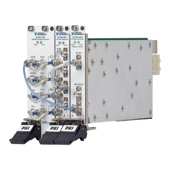
Refer the PXIe-5673 Specifications and PXIe-5673E Specifications documents for the latest module specifications. PXIe-5673 The PXIe-5673 is an RF vector signal generator consisting of the following PXI/PXI Express hardware modules: • PXI-5650/5651/5652—1.3 GHz, 3.3 GHz, or 6.6 GHz local oscillator (LO) source PXI module •... -
Page 6: Features Supported On Pxie-5673/5673E Modules
Express module • PXIe-5450/5451—16 bit, 400 megasample per second (MS/s) arbitrary waveform generator (AWG) PXI Express module • PXIe-5611—6.6 GHz I/Q modulator PXI Express module; NI-RFSG also refers to this module as the Upconverter Note There is no physical device labeled "PXIe-5673E." The PXIe-5673E is the... -
Page 7: Pxie-5673/5673E Block Diagram
Later PXIe-5451 Module, All Revisions No new features 1, 2, 3, 4 Using the PXIe-5611 revision F or later adds improved amplitude settling time to all PXIe-5673/ 5673E devices. PXIe-5673/5673E Block Diagram Refer to the PXI/PXIe-5650/5651/5652, PXIe-5611, and PXIe-5450/5451 block diagram topics for more information about the block diagrams for the individual modules that comprise the PXIe-5673/5673E. - Page 8 PXIe-5673/5673E Device Help Figure 1. PXIe-5673 Block Diagram NI 5673 NI 5450/5451 Digital Analog Digital CH 0+ Filter Output Gain Synchronization Path and Memory Core CH 0– Onboard Waveform Onboard Digital Digital Analog Signal CH 1+ Generation Memory Gain Filter...
- Page 9 PXIe-5673/5673E Device Help Figure 2. PXIe-5673E Block Diagram PXIe-5673E PXIe- 5450/5451 Digital Analog Digital CH 0+ Output Gain Filter Synchronization Path and Memory Core CH 0– Onboard Waveform Onboard Digital Digital Analog Signal CH 1+ Generation Memory Gain Filter Output...
- Page 10 • Commit (or Aborted) - Applies the device's properties or attributes to the hardware. This state also generates an LO signal for the current settings, commits the AWG, and locks Reference Clocks on only the PXIe-5673/5673E Vector Signal Generator. • Generation - In the Generation state, the device is generating a waveform as specified by the session properties or attributes configured.
-
Page 11: System Reference Clock
PXIe-5673/5673E Device Help • To pass triggers between devices, allowing precisely timed responses to asynchronous external events that are being monitored or controlled The number of triggers that an application requires varies with the complexity and number of events involved. -
Page 12: Power On And Reset Conditions
If you enable a PFI line for output, do not connect any external signal source to it; doing so can damage the device, the computer, and the connected equipment. Power On and Reset Conditions The PXIe-5673/5673E hardware is in the following state after powering on or restarting ni.com... - Page 13 PXIe-5673/5673E Device Help the system and allowing the PC operating system and NI-RFSG to fully load. These conditions are also true after a device reset that you perform directly from NI Measurement & Automation Explorer (MAX). • PXIe-5611 I/Q modulator module is powered on.
-
Page 14: Pxie-5673/5673E Front Panel Connectors And Indicators
PXIe-5673/5673E Front Panel Connectors and Indicators This section describes the connectors and LED indicators on the front panels of the PXI or PXI Express hardware modules comprising the PXIe-5673/5673E Vector Signal Generator. Figure 3. PXIe-5673 Front Panel 85 MHz - 6.6 GHz... -
Page 15: Pxie-5450/5451 Front Panel And Leds
PXIe-5673/5673E Device Help Figure 4. PXIe-5673E Front Panel PXIe-5450/5451 Front Panel and LEDs © National Instruments... - Page 16 PXIe-5673/5673E Device Help The following figure shows the PXIe-5450/5451 Waveform Generator front panel, which contains eight connectors and two multicolor LEDs. Figure 5. PXIe-5450 Front Panel ni.com...
- Page 17 PXIe-5673/5673E Device Help Figure 6. PXIe-5451 Front Panel NI PXIe-5451 16-Bit 400 MS/s Arbitrary Waveform Generator ACCESS ACTIVE CLK IN CH 0+ 5 Vp-p MAX, 50 Ω 50 Ω I – CLK OUT CH 0– 0.7 Vp-p NOM 50 Ω...
- Page 18 PXIe-5673/5673E Device Help Connector 5451 front panel. Accepts a trigger from an external source that can start or step PFI 1 through waveform generation or can route signals from several clock, event, and trigger sources. Provides differential waveform output. The signal level on this connector is 1 V , maximum.
-
Page 19: Pxie-5611 I/Q Modulator Front Panel And Leds
Start Trigger. Green—The module has received a Start Trigger and is generating a waveform. Red—The device has detected an error. NI-RFSG must access the device to determine the cause of the error. The LED remains red until the error condition is removed. Errors may include the... - Page 20 PXIe-5673/5673E Device Help Figure 7. PXIe-5611 Front Panel 85 MHz - 6.6 GHz The following table provides connector and use information for the PXIe-5611 front panel connectors. Table 3. General Connector Descriptions Connector Output connector for RF signals. The input impedance is 50 Ω, nominal.
- Page 21 PXIe-5673/5673E Device Help Connector sideband suppressed carrier waveform to modulate the baseband signal applied to the I/Q inputs. Routes the local oscillator output used for combining multiple devices with one common LO source (PXI/PXIe-5650/5651/5652 RF Analog Signal Generator). The output impedance is nominally 50 Ω.
- Page 22 PXIe-5673/5673E Device Help properly connected. If one or more of these connections are not correctly made, common-mode errors cause the PXIe-5673/5673E Vector Signal Generator to be uncalibrated. The following table provides LED and indications information for the PXIe-5611 I/Q modulator module front panel LEDs.
-
Page 23: Pxi/Pxie-5650/5651/5652 Front Panel And Leds
PXIe-5673/5673E Device Help Indications • I/Q overvoltage protection fault—The I/Q inputs exceed the maximum voltage. I and Q inputs are disabled in order to protect the device. PXI/PXIe-5650/5651/5652 Front Panel and LEDs The PXI/PXIe-5650/5651/5652 RF Analog Signal Generator is available with either two or three front panel connectors. - Page 24 Routes the reference signal to and from the PXIe-5650/5651/5652. Maximum damaging level is 10 VDC. REF IN/OUT has an input impedance of 50 Ω. NI recommends that a high impedance source is not used to provide a reference signal. A high impedance source can...
- Page 25 PXIe-5673/5673E Device Help Indications are being written to in order to control the device. GREEN—The module is ready to be programmed. Indicates the state of the PXIe-5650/5651/5652 module: Off—The module is not generating a signal. Amber—The module PLLs are attempting to lock.
- Page 26 Routes the reference signal to and from the PXIe-5650/5651/5652. Maximum damaging level is 10 VDC. REF IN/OUT has an input impedance of 50 Ω. NI recommends that a high impedance source is not used to provide a reference signal. A high impedance source can...
-
Page 27: Ref In/Out Connector
PXIe-5673/5673E Device Help Connector MHz reference signal. The following table provides information about the PXI-5650/5651/5652 module front panel LEDs and the device states they indicate: Table 8. LED Indicators Indications Indicates the basic hardware status of the PXI-5650/5651/5652 module. OFF—The module is not yet functional or has detected a problem with a PXI power rail. - Page 28 The ability to export or import the reference signal makes it possible to frequency-lock NI RF devices together using one as the master.
-
Page 29: Pxie-5450/5451 Waveform Generator
PXIe-5673/5673E Device Help PXIe-5450/5451 Waveform Generator The PXIe-5450/5451 is a dual-channel, 400 MS/s, 16-bit arbitrary waveform generator (AWG) PXI Express module. This section contains information about the PXIe-5450/5451 AWG module when used with the PXIe-5611 I/Q Modulator and the PXI/PXIe-5650/5651/5652 RF Analog Signal Generator. -
Page 30: Memory Options
PXIe-5673/5673E Device Help • Onboard Memory stores the waveform data and scripts that you load into the device. • Clocking allows you to create your Sample Clock and Reference Clock. • The Waveform Generation Engine retrieves the waveform data and instructions from the Onboard Memory using the Sample Clock. -
Page 31: Pxie-5611 Block Diagram
PXIe-5673/5673E Device Help PXIe-5611 Block Diagram This topic contains information about the PXIe-5611 I/Q Modulator top-level block diagram and descriptions of the individual blocks. Figure 9. PXIe-5611 Block Diagram I– Q– Complex Modulation Coarse RF Pulse Power Conditioning Modulation Baseband... -
Page 32: Baseband Input Protection
When no signal is applied to the PLS MOD connector and pulse modulation is disabled, the RF OUT signal operates normally. You can use NI-RFSG to enable pulse modulation. Complex Modulation Complex modulation is the core function of the PXIe-5611 I/Q Modulator. Complex... -
Page 33: Rf Filtering
The PXIe-5611 LO IN to LO OUT gain is characterized at NI during the manufacturing process or during an annual external calibration. The calibration procedure involves the use of a power meter. When the proper gain is measured, it is stored on the PXIe-5611 where it is used to correct each generated signal. -
Page 34: Lo Signal Conditioning
You can assign the anticipated input power at the PXIe-5611 LO IN front panel connector using NI-RFSG so that the PXIe-5611 returns 0 dBm of power. Refer to the specifications document specific to your device for information about the expected level accuracy. -
Page 35: Rf Out Power Conditioning
The effects of temperature drift are automatically compensated for each time an NI-RFSG VI or function is called that adjusts the configuration of the device. - Page 36 Querying the value of the device temperature using NI-RFSG returns the temperature within the NI 5611 RF enclosure. A second temperature sensor is located outside the RF enclosure, but this sensor is not readable with NI-RFSG. If this sensor reads unsafe temperatures, it shuts down the device power rails to power off the RF enclosure and protects the RF circuitry from damage.
-
Page 37: Pxi/Pxie-5650/5651/5652 Rf Analog Signal Generators
PXIe-5673/5673E Device Help PXI/PXIe-5650/5651/5652 RF Analog Signal Generators PXI/PXIe-5650/5651/5652 Block Diagram This topic contains information about the PXI/PXIe-5650/5651/5652 RF Analog Signal Generator top-level block diagram and descriptions of the individual blocks. The system control unit manages the control signals and data transferred between the circuit blocks. -
Page 38: Power On And Reset Conditions
The PXI/PXIe-5650/5651/5652 RF Analog Signal Generator hardware is in the following state after powering on or restarting the system and allowing the PC operating system and NI-RFSG to fully load. These conditions are also true after a device reset that you perform directly from NI Measurement & Automation Explorer (MAX). -
Page 39: Power Level Adjustment
The ALC is calibrated for amplitude and temperature variation and is used to control the upper 10 dB. When possible, NI-RFSG uses only the ALC to get the specified power. However, if more than 10 dB of attenuation is needed at the specified frequency , then the attenuators are used. -
Page 40: Frequency-Shift Keying (Fsk)
• 10 ≤ m ≤ 1,020 (for square modulation waveforms) • m is the number of samples per waveform, which is optimized by NI-RFSG to produce the most linear waveform for a desired rate. Also, m is always an even number for the FM rate calculation. -
Page 41: On-Off Keying (Ook)
PXIe-5673/5673E Device Help NI-RFSG calculates the exact symbol rate and FSK deviation, which can differ slightly from the input parameters. For user-defined bit streams, the valid symbol rate range and bit stream length are determined by the following relations: 1 ≤ bit stream length ≤ 1,022 Symbol rate = 50 MHz / (n ×... - Page 42 PXIe-5673/5673E Device Help signal power to the lowest possible level for this frequency. During a bit value of 1 (high power level), the PXI/PXIe-5650/5651/5652 bypasses the main attenuators. Therefore, the high power level range is limited by the power level range of the ALC.
-
Page 43: Phase Modulation (Pm)
• 10 ≤ m ≤ 1,020 (for square modulation waveforms) • m is the number of samples per waveform, which is optimized by NI-RFSG to produce the most linear waveform for a desired rate. Also, m is always an even number for the PM rate calculation. -
Page 44: Modulation Implementation
• Internal modulation waveform types: user-defined bit stream or pseudorandom bit sequence (PRBS) • Symbol rate NI-RFSG calculates the exact symbol rate and PSK deviation, which can differ slightly from the input parameters. For user-defined bit streams, the valid symbol rate range and bit stream length are determined by the following relations: 1 ≤... -
Page 45: Sinusoidal Tone Versus Modulation Operation
PXIe-5673/5673E Device Help single tone (sine) generation, NI-RFSG selects the low loop bandwidth for the best possible phase noise performance. The specified phase noise is based on low loop bandwidth. Using NI-RFSG, you can select wide loop bandwidth, which trades off phase noise between 3 kHz to 300 kHz offsets for faster tuning times. -
Page 46: Thermal Shutdown
Thermal Shutdown NI-RFSG supports thermal shutdown monitoring for NI RF signal generator modules. This feature allows the module to detect when it has reached a dangerously high temperature and to then power off, preventing damage to the device. -
Page 47: Frequency Tuning Times
PXIe-5673/5673E Device Help If safe temperature limits are exceeded, the RF enclosure is powered off, and NI-RFSG returns an error. Note The PXIe-5673/5673E is warm to the touch during normal operation. The device should never reach a temperature high enough to cause thermal shutdown unless the fan or vents on the PXI or PXI Express chassis are blocked or the filters on the fans are excessively dusty. -
Page 48: Pxi/Pxie-5650/5651/5652 Noise Floor And Signal-To-Noise Ratio
-173.8 dBm/Hz at room temperature. Beyond this limit, the SNR decreases one-to-one with signal level. PXI/PXIe-5650/5651/5652 Factory Calibration NI performs calibration of the PXI/PXIe-5650/5651/5652 that is relative to an NIST- traceable standard over the specified operating temperature range. Calibration ni.com... -
Page 49: Device Warm-Up
PXI/PXIe-5650/5651/5652 RF enclosure. Device Warm-Up NI recommends warming up the PXI/PXIe-5650/5651/5652 hardware for 30 minutes before operation. The unit is fully functional prior to this time, but frequency, amplitude accuracy, and other specifications are not at warranted levels until the device has fully completed warming up. - Page 50 PXIe-5673/5673E Device Help Note Warm up begins when the PXI or PXI Express chassis has been powered on and the operating system has completely loaded. ni.com...
-
Page 51: Generation Modes
Generation Modes The PXIe-5673/5673E has the following three available generation modes: • CW mode—NI-RFSG software internally generates a continuous-wave signal (a sine tone). In this mode, a DC signal is returned from the AWG, and the I/Q modulator provides a fixed amplitude and phase adjustment to the LO signal to produce the RF OUT signal. -
Page 52: Peer-To-Peer Data Streaming
• Reader Peer—The peer receiving the data over the bus from the writer peer. NI RF signal generators assume the role of the reader peer endpoint in a peer-to-peer stream because they read data from the writer peer through the peer-to-peer stream and then pass the data to physical channels. -
Page 53: Configuring A Peer-To-Peer Stream
Configuring a Peer-to-Peer Stream To configure a peer-to-peer stream using the NI-P2P API, a writer and reader handle for each endpoint are required. Use Get Stream Endpoint Handle to generate a reader endpoint handle. Configuring Flow Control When streaming data between two peers, the writer peer must have flow control credits to move data over the bus to the reader peer. - Page 54 Write P2P Endpoint (I16) VI or the niRFSG_WriteP2PEndpointI16 function or from a previous streaming operation. In this case, NI-RFSG adjusts the default initial credits to issue, at most, the difference between the endpoint depth and the amount of data already in the endpoint.
- Page 55 PXIe-5673/5673E Device Help The following three methods are available for preparing the RF signal generator endpoint for startup: • P2P Endpoint Fullness Start Trigger Level property or NIRFSG_ATTR_P2P_ENDPOINT_FULLNESS_START_TRIGGER_LEVEL attribute—Starts generation after the endpoint receives the specified number of samples. If no number of samples is specified, the driver automatically selects an appropriate value.
- Page 56 Applications between two NI devices, linked using NI-P2P, automatically use this behavior. 2. Finite Generation (stream n)—If the RF signal generator receives the specified number of samples from the writer peer, the NI-RFSG session completes without an underflow error. ni.com...
- Page 57 • User-Requested Abort—Using the niRFSG Abort VI or niRFSG_Abort function, the NI-RFSG session does not return an error and the niRFSG Check Generation Status VI or niRFSG_CheckGenerationStatus returns TRUE for Done. However, if the writer peer is not configured carefully for this event, it may overflow because the RF signal generator is no longer allowing it to send data through the stream.
- Page 58 PXIe-5673/5673E Device Help method to determine if all data was sent. Reconfiguring a Stream Consider the following scenarios when reconfiguring an NI-RFSG session for peer-to- peer data streaming. • If the generation from the previous session completed with Done Notification, the stream remains linked, but it is disabled.
-
Page 59: Advanced Pxie-5673 Configuration
Advanced PXIe-5673 Configuration Interconnecting Multiple PXIe-5673 Modules The NI RF Signal Generators Getting Started Guide explains how to set up one PXIe-5673 Vector Signal Generator. NI-RFSG supports connecting multiple PXIe-5673 modules such as two PXIe-5611 I/Q Modulators and two PXIe-5450 Waveform Generators, as shown in the following figure. -
Page 60: Timing Configurations For Pxie-5673 Modules
PXIe-5673/5673E Device Help Complete the following steps to interconnect multiple PXIe-5673 modules: 1. Install an additional PXIe-5611 immediately to the left of the previously installed PXIe-5450. 2. Install an additional PXIe-5450 immediately to the left of the PXIe-5611 installed in step 1. - Page 61 • PXI 10 MHz Backplane Clock Configuring Internal Reference Clock Timing The default configuration of the PXIe-5673 is for the PXI-5650/5651/5652 to export its internal Reference Clock to the PXIe-5450/5451 so that the PXIe-5450/5451 and the PXI-5650/5651/5652 devices are frequency-locked.
- Page 62 PXIe-5673/5673E Device Help To configure the PXIe-5673 to use the internal clock, set the Reference Clock Source property to OnBoardClock or the NIRFSG_ATTR_REF_CLOCK_SOURCE attribute to NIRFSG_VAL_ONBOARD_CLOCK_STR. Configuring External Reference Clock Timing You can also configure the PXIe-5673 to lock to an external reference source.
- Page 63 50 Ω. Configuring PXI 10 MHz Backplane Clock Timing You can also configure the PXIe-5673 to lock to the PXI 10 MHz backplane clock. The configuration shown in the following figure locks the PXIe-5650/5651/5652 and PXIe-5450 to the PXI 10 MHz reference. Locking to the PXI 10 MHz reference does not require a cable, but this configuration does not provide the same frequency and phase noise performance as the PXI-5650/5651/5652 internal Reference Clock.
-
Page 64: Connecting The Pxie-5673 To The Pxie-5663
PXIe-5673/5673E Device Help To configure the PXIe-5673 to use the PXI 10 MHz backplane clock, set the Reference Clock Source property to PXI_CLK or the NIRFSG_ATTR_REF_CLOCK_SOURCE attribute to NIRFSG_VAL_PXI_CLK_STR. Connecting the PXIe-5673 to the PXIe-5663 You can use the PXIe-5673 Vector Signal Generator with the PXIe-5663 Vector Signal Analyzer to utilize generation and analysis of communications signals from DC to 6.6 GHz. - Page 65 PXIe-5673/5673E Device Help Complete the following steps to connect the PXIe-5673 and PXIe-5663 to use an external clock: 1. Install the PXI-5652 RF Analog Signal Generator that shipped with the PXIe-5663 immediately next to the PXI-5650/5651/5652 device already installed for the PXIe-5673.
- Page 66 9. Use a flexible cable to connect the REF IN/OUT connector on the PXI-5650/5651/ 5652 device already installed for the PXIe-5673 to an open connector on a 3-way splitter. 10. Use a flexible cable to connect the CLK In connector on the PXIe-5622 to an open connector on a three-way splitter.
- Page 67 REF IN/OUT connector on the PXI-5650/5651/5652. 2. Install the PXI-5652 device that shipped with the PXIe-5663 immediately next to the PXI-5650/5651/5652 device already installed for the PXIe-5673. 3. Install the PXIe-5601 device that shipped with the PXIe-5663 immediately next to the PXI-5650/5651/5652 device installed in step 1.
-
Page 68: Advanced Pxie-5673E Configuration
Advanced PXIe-5673E Configuration Interconnecting Multiple PXIe-5673E Modules The NI PXIe-5673E Getting Started Guide explains how to set up one PXIe-5673E Vector Signal Generator. NI-RFSG supports connecting multiple PXIe-5673E devices such as two PXIe-5611 I/Q Modulators and two PXIe-5450/5451 Waveform Generators, as shown in the following figure. -
Page 69: Timing Configurations For Pxie-5673E Modules
PXIe-5673/5673E Device Help 1. Install an additional PXIe-5611 immediately to the left of thepreviously installed PXIe-5450/5451. 2. Install an additional PXIe-5450/5451 immediately to the left of the PXIe-5611 installed in step 1. 3. Use Cable A to connect the CH 1-/Q- connector on the PXIe-5450/5451 installed in step 2 to the Q- connector on the PXIe-5611 installed in step 1. - Page 70 PXIe-5673/5673E Device Help sources are available: • Internal Reference Clock • External Reference Clock • PXI Express 10 MHz Backplane Clock Note The following timing configurations are for PXIe-5673E hardware modules that include the PXIe-5650/5651/5652 with three front panel connectors.
-
Page 71: Connecting The Pxie-5673E To The Pxie-5663E
Using an internal clock results in a low phase noise degrading below 1 kHz offset. This impacts communication signals with symbol captures longer than 1 ms. For best device performance, NI recommends using an external Reference Clock. Complete the following steps to use an internal or external clock with the PXIe-5673E and PXIe-5663E. - Page 72 PXIe-5673/5673E Device Help Complete the following steps to connect the PXIe-5673E and PXIe-5663E to use an external clock: 1. Install the PXIe-5652 device that shipped with your PXIe-5663E immediately next to the PXIe-5650/5651/5652 device already installed for the PXIe-5673E. 2. Install the PXIe-5601 device that shipped with your PXIe-5663E immediately next to the PXIe-5652 device installed in step 1.
- Page 73 PXIe-5673/5673E Device Help OUT connector on the PXIe-5601. Configuring an External Reference Clock After interconnecting the PXIe-5673E and PXIe-5663E devices, complete the following steps to allow both devices to share an external Reference Clock source. 1. When programming the PXIe-5673E, set the output terminal parameter of the niRFSG Export Signal VI to CLK OUT or set the outputTerminal parameter of the niRFSG_ExportSignal function to NIRFSG_VAL_CLK_OUT_STR.
-
Page 74: External Lo
LO, the NI-RFSG session controls the I/Q modulator and the AWG, but the LO source is not controlled by the NI-RFSG session. An external LO is useful if you have an LO with lower phase noise, lower harmonics, or faster tuning time than the PXI/ PXIe-5650/5651/5652. -
Page 75: Shared Lo
PXIe-5673/5673E Device Help Controlling the PXIe-5673/5673E with an External LO Complete the following steps to control the PXIe-5673/5673E with an external LO by setting the appropriate frequency and power level: 1. Specify the LO frequency to the NI-RFSG session using the Frequency property or NIRFSG_ATTR_FREQUENCY attribute. - Page 76 Phase offset is the difference between the phases of two or more signals. You can achieve phase coherency on the PXIe-5673/5673E by using a shared LO. Phase coherency is guaranteed because a single LO is shared between each PXIe-5673/5673E module in the daisy chain.
- Page 77 PXIe-5673/5673E Device Help MIMO Systems Multiple-input, multiple-output (MIMO) systems, such as when you share an LO, improve the overall bit error rate in the presence of multipath performance and increase throughput, but there are some implications on dynamic range. When sharing an LO, the broadband noise of the LO signal increases slightly as it passes through each PXIe-5611 I/Q Modulator.
-
Page 78: Rf Power Level Adjustment
The AWG module provides fine signal power adjustment by scaling the digital waveform. NI-RFSG automatically selects the scaling factor based on signal power requirements. NI-RFSG modifies the digital waveform such that it does not occupy the full-scale output voltage of the DAC. At the lowest requested power levels, the PXIe-5611 uses all of its available attenuation, and the remaining power is removed from the AWG module. - Page 79 Attenuator Hold The attenuator hold feature allows you to adjust the output level without switching the internal attenuators on the RF vector signal generator. To achieve this, NI-RFSG sets the PXI-5610 RF Signal Upconverter and PXIe-5611 I/Q Modulator to the...
-
Page 80: Understanding Pxie-5673/5673E Specifications And Performance
Performance This section contains information for the user who wants to optimize performance of the PXIe-5673/5673E Vector Signal Generator by better understanding the common specification characteristics of the device. Refer to the specifications document specific to your device for detailed device specifications. - Page 81 Intermixing occurs among the generated tones to produce spurs. The most prevalent type of IMD seen at the output of the PXIe-5673/5673E is the third order IMD (IMD3). For example, in the case of two tones generating at frequencies f...
- Page 82 PXIe-5611 RF OUT front panel connector by 1 dB and that of the IMD products by 3 dB (for a total of 2 dBc improvement, assuming the output power is low enough so that the modulators dominate the IMD performance of the PXIe-5673/ 5673E).
- Page 83 RF image occurs mostly due to phase skew and/or gain imbalance in the I and Q paths at baseband frequency. RF image degrades over baseband frequency. Manually calibrating the PXIe-5673/5673E in addition to calibration performed at NI can reduce RF image.
- Page 84 PXIe-5673/5673E Device Help carrier frequency. For example, a single-sideband +10 MHz signal generated at a carrier of 1 GHz produces a desired signal at the RF OUT connector at 1,010 MHz. A baseband feedthrough signal also appears at the RF OUT connector at 10 MHz. The following...
-
Page 85: Effects Of Non-Ideal Reflection Coefficients On Delivered Power
PXIe-5673/5673E Device Help Reducing the Spur Level You can reduce the level of the spur by completing the following steps: 1. Set the Power Level Type property to Peak Power or the NIRFSG_ATTR_POWER_LEVEL_TYPE attribute to NIRFSG_VAL_PEAK_POWER. 2. Set the Software Scaling Factor property or NIRFSG_ATTR_ARB_WAVEFORM_SOFTWARE_SCALING_FACTOR attribute to less than 1. - Page 86 PXIe-5673/5673E Device Help device's impedance as seen by the PXIe-5611 RF OUT or LO OUT front panel connectors from an ideal 50 Ω. When an external load is connected to either the PXIe-5611 RF OUT or LO OUT front panel connector, the accuracy of the power delivered to the external load depends on the external load's LO OUT and RF OUT reflection coefficient(Γ...
-
Page 87: Settling Times
To allow for maximum user flexibility, NI-RFSG does not account for the amount of time required to settle to the final power level. NI-RFSG does not impose wait times at © National Instruments... - Page 88 0 dBm. To avoid waiting for the attenuators to settle, especially when running power sweeps, enable attenuator hold. Enabling attenuator hold sets the gain level of the PXIe-5673 signal path to accommodate the maximum power to be generated and sweeps power by rescaling the digital data.
- Page 89 Refer to the specifications document specific to your device for more information about frequency resolution. The following table summarizes the LO signal paths on the PXIe-5673/5673E. LO Signal Path Lowest Carrier Frequency (MHz) Highest Carrier Frequency (MHz) 85.0...
-
Page 90: Settling Times For Previous Modules
NI-RFSG does not impose long wait times. However, when power accuracy is critical, deliberate wait periods should be added following any change in setting the amplitude or frequency of the PXIe-5673 Vector Signal Generator. - Page 91 PXIe-5673/5673E Device Help meet a newly-set power level and the same carrier frequency, the PXIe-5673 switches attenuators in its signal path. The PXIe-5673 uses high-performance gallium arsenide (GaAs) attenuators that allow the device to achieve good performance, but GaAs attenuators require relatively long times to settle.
- Page 92 PXIe-5673/5673E Device Help added when the PXIe-5673 carrier frequency encounters an RF filter change. The appropriate signal path is selected according to the coerced carrier frequency and the selected signal path cannot be overridden. Refer to the specifications document specific to your device for more information about frequency resolution. The following table summarizes the LO signal paths on the PXIe-5673.
-
Page 93: Identifying Module Revision
PXIe-5673/5673E Device Help Identifying Module Revision PXIe-5611 specifications and features may vary according to the revision letter of the module. To determine the revision letter of your PXIe-5611, query the Module Revision property or the NIRFSG_ATTR_MODULE_REVISION attribute. You can also find the module revision by referring to the module part number, which is printed on your module and consists of six digits and one letter followed by an additional two digits. -
Page 94: Impairment Calibration
PXIe-5673/5673E Device Help Impairment Calibration I/Q impairments, such as I offset, Q offset, I/Q gain imbalance and I/Q phase skew, degrade the spurious performance of the I/Q modulator. The offsets contribute to carrier suppression. Gain imbalance and phase skew contribute to the creation of an image for the single-sideband RF signal output that is mirrored across the carrier.For a... -
Page 95: Improving Carrier And Image Rejection Performance
3. Observe the resulting spectrum and identify the generated signal along with its image and LO leakage. 4. Adjust the impairments using the appropriate properties or attributes to reduce their effects. For example, reduce the LO leakage and the image of the PXIe-5673/ © National Instruments... - Page 96 With the RF vector signal analyzer, locate the generated signal at exactly 1.001 GHz (if the device is locked in frequency with the PXIe-5673/5673E), the leaked LO at 1 GHz and the image at 0.999 GHz. Make sure the image and the leaked LO are at least 20 dB or 30 dB above the displayed noise floor.
-
Page 97: Modulation Bandwidth Performance
1 MHz from the carrier. As the modulation bandwidth increases, the image performance degrades. At ±10 MHz baseband bandwidth, the image at the RF OUT connector of the PXIe-5673/ 5673E is still within a few dB from its specified performance at ±1 MHz offset. Refer to the device specifications for information about expected performance. -
Page 98: Interpolation Settings
PXIe-5673/5673E Device Help Interpolation Settings To determine the total interpolation, divide 400 MS/s by your sample rate and round down to the nearest integer (or the nearest "step," as noted in the Interpolation table for your total interpolation value). Then, consult the following table for settings that will allow you to achieve your desired interpolated sample rate. -
Page 99: Compression
Compression Compression describes the higher output power region of an amplifier where the amplifier's gain becomes non-linear. The PXIe-5673/5673E Vector Signal Generator begins to enter its compression region as output power levels increase above 0 dBm. The effects of this compression can be observed as a decreased TOI point and increased intermodulation and harmonic tones. - Page 100 PXIe-5673/5673E Device Help NIRFSG_ATTR_POWER_LEVEL_TYPE attribute to NIRFSG_VAL_AVERAGE_POWER, reducing the power level at the RF OUT front panel connector, for example, from 1 dBm to 0 dBm reduces the carrier suppression by 1 dB. Subsequently, the carrier suppression to the desired RF output power ratio is mostly maintained, in dBc.
-
Page 101: Hardware Integration And Maintenance
PXIe-5673/5673E Device Help Hardware Integration and Maintenance This section contains information about integrating and maintaining NI-RFSG devices into a PXI- or PXI Express-based measurement system. The PXI architecture has built-in timing and triggering features that can synchronize multiple devices over a backplane timing bus. Multiple devices in a modular... - Page 102 PXIe-5673/5673E Device Help Figure 10. PXI Express Module Installation Chassis Guidelines You can install NI PXI Express modules in the following PXI Express chassis slots: • PXI hybrid slots—Accepts either PXI modules that are hybrid slot-compatible or PXI Express modules •...
-
Page 103: Uninstalling The Hardware
PXIe-5673/5673E Device Help Uninstalling the Hardware Hot Surface If the module has been in use, it may exceed safe handling temperatures and cause burns. Allow the module to cool before removing it from the chassis. Notice Disconnect or disable any external RF, clock, or digital connections to the device front panel.
Need help?
Do you have a question about the PXIe-5673 and is the answer not in the manual?
Questions and answers