Table of Contents
Advertisement
Quick Links
Advertisement
Table of Contents

Subscribe to Our Youtube Channel
Related Manuals for NI PXIe-5641


Summary of Contents for NI PXIe-5641
- Page 1 PXIe-5641 Getting Started 2024-03-27...
-
Page 2: Table Of Contents
NI-5640R Instrument Driver Examples........13... - Page 3 Appendix A: NI PXIe-5641R Front Panels........
-
Page 4: Getting Started Guide Ni If Transceiver
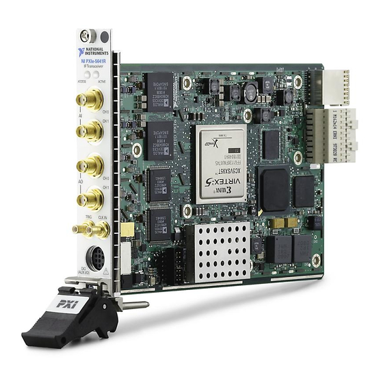
PXIe-5641 Getting Started Getting Started Guide NI IF Transceiver This document explains how to install, configure, and program an NI PXIe-5641R IF transceiver. The NI 5641R offers two 100 MS/s, 14-bit input channels with built-in digital downconversion and two 200 MS/s, 14-bit output channels with built-in digital upconversion. -
Page 5: Verifying The Kit Contents
LabVIEW FPGA Module Using the LabVIEW FPGA module, you can program the NI 5641R FPGA to match the requirements of your system. Using LabVIEW FPGA, you can create user-defined behavior for the NI 5641R using a virtual instrument (VI), thereby creating an application-specific I/O device. -
Page 6: Ni-5640R Asynchronous Programming Palette
NI-5640R Asynchronous Programming Palette You can use the NI-5640R Asynchronous Programming palette, an additional palette of LabVIEW FPGA nodes, to simplify creating LabVIEW FPGA applications for your NI 5641R. Using the asynchronous programming model provides free-running actors that can execute independently of the dataflow dependencies created by traditional LabVIEW programming. - Page 7 PXIe-5641 Getting Started Programming Methods Comparison Table 1. NI 5641R Programming Methods Comparison Feature LabVIEW FPGA Module NI-5640R LabVIEW Instrument Driver Traditional LabVIEW NI-5640R FPGA Asynchronous Programming Programming Advanced LabVIEW and LabVIEW FPGA Easy-to-use application Complexity programming skills required. Using the LabVIEW...
-
Page 8: Installing Labview And Ni-5640R Software
Installing LabVIEW and NI-5640R Software You must be an Administrator to install NI software on your computer. Select your programming method before you install your ADE. 1. Install LabVIEW. 2. If you choose to use the LabVIEW FPGA programming method, install the LabVIEW FPGA Module. - Page 9 PXIe-5641 Getting Started 4. Remove the black plastic covers from all the captive screws on the module front panel. 5. Identify the slots you will use in the chassis. The following figure shows the symbols that indicate the slot types.
-
Page 10: Configuring The Ni 5641R In Max
Configuring the NI 5641R in MAX Use Measurement & Automation Explorer (MAX) to configure your NI hardware. MAX informs other programs about which NI hardware products are in the system and how they are configured. MAX is automatically installed with NI-5640R. -
Page 11: Connecting Analog Input (Ai) Signals
PXIe-5641 Getting Started You can connect three kinds of signals to the NI 5641R: analog input (AI) signals, analog output AO) signals, and digital input/output (DIO) signals. Related reference: Appendix A: NI PXIe-5641R Front Panels ■ Connecting Analog Input (AI) Signals Use a connector saver (a replaceable SMA adapter used on test equipment) ■... -
Page 12: Connecting Digital Input/Output (Dio) Signals
NI IF Transceivers Help for more information about imaging. Connecting Digital Input/Output (DIO) Signals The NI 5641R front panel DIO connector has nine pins. The DIO lines are direction- configurable by pin as input or output. If you are using LabVIEW FPGA, you can write an application to customize the functionality of this connector for your application. -
Page 13: Programming The Ni 5641R
Do not connect the +5 V power pins directly to analog or digital ground or to any other voltage source on the NI 5641R or any other device under any circumstance. Doing so can damage the NI device and the host computer or chassis. -
Page 14: Re-Enabling A Device After Thermal Shutdown
The ambient temperature around the chassis is too high. This condition may be caused by high ambient air temperature or proximity to heat-generating devices. Ensure the NI 5641R is not installed Slot 7 or 8 in an eight-slot chassis. If it is, ■ move the module to a different slot. -
Page 15: My Signal Looks Very Noisy
For more information about avoiding alias effects, refer to the Alias Effects ■ topic for your device in the NI IF Transceivers Help.For more information about avoiding alias effects, refer to the Alias Effects topic for your device in the NI IF Transceivers Help. -
Page 16: Control Function In Labview Fpga
PXIe-5641 Getting Started It Takes a Long Time to Access Controls and Indicators Using the Read/Write Control Function in LabVIEW FPGA When you select the Read/Write Control function in LabVIEW FPGA, LabVIEW locates the corresponding controls and indicators in your FPGA VI. If your FPGA VI is not loaded into memory at this time, LabVIEW loads it now and unloads it after the operation completes. -
Page 17: Filename.lvbitx
PXIe-5641 Getting Started 1. Place the control or indicator in a clock domain that is faster, such as the default Top-Level Clock. 2. Use global variables to transfer the value to a slower clock domain, as shown in the following figure. -
Page 18: When I Run An Fpga Vi, A Compilation Error Instantly Occurs
PXIe-5641 Getting Started 2. If you are using the Open FGPA VI Reference function in dynamic mode (configured by selecting the Dynamic mode checkbox in the Configure Open FPGA VI Reference dialog box), you do not need to bind the FPGA host reference to the type definition. -
Page 19: Connecting Two Asynchronous Data Wires Produces A Broken Wire
FIFO. Related information: Refer to the Data Exchange Policies section of the NI IF Transceivers Help for ■ more information about the types of data exchange policies.Refer to the Data Exchange Policies section of the NI IF Transceivers Help for more information about the types of data exchange policies. -
Page 20: Appendix A: Ni Pxie-5641R Front Panels
PXIe-5641 Getting Started Appendix A: NI PXIe-5641R Front Panels The NI 5641R front panels contain seven connectors—four SMA jack connectors, two SMB connectors, and one 9-pin mini-circular DIN connector. Figure 5. NI PXIe-5641R Front Panel Connectors Table 3. NI 5641R Connectors... - Page 21 PXIe-5641 Getting Started Connector Name Type Description CLK IN Input terminal for an external Reference or Sample Clock. TRIG Input or output terminal for device trigger signals. DIO (AUX) 9-pin DIN mini-circular Input or output terminal for device digital I/O (DIO) channels.
-
Page 22: Appendix B: Creating An If Transceiver Application In Labview
You can program the NI 5641R using LabVIEW FPGA or the NI-5640R instrument driver. Creating an Application Using LabVIEW FPGA To develop and use an FPGA VI with the NI 5641R, you must complete four major steps. 1. Create the LabVIEW project. -
Page 23: Creating A Project Using The Ni5640R Template
The following sections walk you through creating a simple spectrum analyzer using one of the analog input channels on the NI 5641R. You can configure the center frequency and the bandwidth to analyze. The application also generates a sine tone that can be used as the signal to analyze. -
Page 24: Developing The Fpga Vi
FPGA VI. Note Asynchronous programming works only on the NI PCI-5640R and NI PXIe-5641R targets and should not be used for code you may need to adapt for other classes of LabVIEW FPGA targets. Adding Resources to the Project To use traditional LabVIEW FPGA programming to develop the FPGA VI, all resources used by the FPGA VI must be added to the project. -
Page 25: Developing Your Fpga Vi
PXIe-5641 Getting Started The New FPGA I/O dialog box appears and displays the I/O resources available on the NI 5641R. 2. In the New FPGA I/O dialog box, expand Analog Input. 3. Select ADC_0_Port_A_I and ADC_0_Port_A_Q. 4. Click the right arrow to add these resources to the New FPGA I/O table. - Page 26 PXIe-5641 Getting Started 3. Wire a FALSE constant to the Loop Condition terminal. 4. Select both Analog Input FPGA I/O items in the Project Explorer window and drag them onto the block diagram inside the timed loop you created. Two FPGA I/O Nodes appear on the block diagram configured with the specific FPGA I/O item.
- Page 27 PXIe-5641 Getting Started 8. Wire the outputs of the FPGA I/O Nodes to the inputs of the Join Numbers function. 9. Wire the output of the Join Numbers function to the Element input of the FIFO. 10. Create a numeric constant of 0 and wire it to the Timeout input of the FIFO.
-
Page 28: Specifying How Often To Acquire I And Q Samples
PXIe-5641 Getting Started Spectrum Analyzer folder created in step 1 of Using the ni5640R Template. e. Click OK and close the VI. f. Return to the block diagram for your My Simple Spectrum Analyzer (FPGA).vi and right-click the second global variable node. - Page 29 PXIe-5641 Getting Started 5. Wire a FALSE constant to the Loop Condition terminal. 6. Copy the Acquire and Timed Out? global variables and place them inside the new Timed Loop created in step 4. 7. Right-click the Acquire global variable and select Change to Write.
-
Page 30: Using The Ni-5640R Asynchronous Programming Palette
Skip to the Compiling the FPGA VI section for the next steps you should take. Using the NI-5640R Asynchronous Programming Palette Before using the NI-5640R Asynchronous Programming palette, complete all the steps in the Using the ni5640R Template section. 1. Double-click the My Simple Spectrum Analyzer(FPGA).vi to open the VI and then open the block diagram. - Page 31 11. Place a Write Accessor node in the While Loop to the right of the Acquire control. The Write Accessor node is located on the Functions palette under NI-5640R Asynchronous Programming. 12. Wire the Acquire control to the Write Accessor node.
- Page 32 PXIe-5641 Getting Started The DMA to Host node is located on the Functions palette under NI-5640R Asynchronous Programming. 18. Click the DMA FIFO glyph on the DMA to Host node to launch the Configure Target to Host dialog box and make the changes shown in the following figure.
-
Page 33: Ni-5640R Fpga And Asynchronous Programming Examples
NI-5640R FPGA and Asynchronous Programming Examples The NI-5640R FPGA and asynchronous programming examples demonstrate some of the functionality of the NI IF transceiver that you can use or integrate into your applications. These examples serve as interactive tools, programming models, and building blocks for your own applications. -
Page 34: Developing The Host Vi
To communicate programmatically with the FPGA VI, you must develop a host VI that runs on a Windows or an RT target. The host VI communicates with the FPGA VI running on the NI 5641R. Opening a Reference to the FPGA VI 1. -
Page 35: Adding Ni-5640R Vis
PXIe-5641 Getting Started 3. Right-click the Open FPGA VI Reference function and select Configure Open FPGA VI Reference. 4. Select the VI button to launch the Select VI dialog box. 5. Select the My Simple Spectrum Analyzer (FPGA) VI you created in the Developing the FPGA VI section. - Page 36 PXIe-5641 Getting Started 1. Place an Invoke Method function on the block diagram to the right of the ni5640R DAC Config for Single Tone VI. The Invoke Method function is available on the Functions » FPGA Interface palette. 2. Wire the Invoke Method function to the ni5640R DAC Config for Single Tone VI.
-
Page 37: Analyzing The Data
PXIe-5641 Getting Started Figure 14. Wiring the FPGA VI for Data Acquisition Analyzing the Data 1. Place a Split Number VI on the block diagram to the right of the Invoke Method Node you placed and wired in step 9 in the preceding section. -
Page 38: Adding Controls And Indicators
PXIe-5641 Getting Started Figure 15. Analyzing the Data Adding Controls and Indicators 1. Add the following controls and indicators, as shown in the following figure: Decimation—Specifies how much decimation is performed on the ■ analog input signal. This control determines the maximum bandwidth of your signal. - Page 39 PXIe-5641 Getting Started 2. Place a Simple Error Handler VI on your block diagram. The Simple Error Handler VI is available on the Functions palette under Programming » Dialog & User Interface. 3. Wire the Close FPGA VI Reference function to the Simple Error Handler VI.
- Page 40 5. Populate your application with the control values shown in the Host VI Front Panel . 6. On the NI 5641R front panel, connect the AO 0 connector to the AI 0 connector using an SMA-to-SMA cable so that the output tone from AO 0 is fed into AI 0.
-
Page 41: Creating An Application Using The Ni-5640R Instrument Driver
Locating Examples You can use the NI Example Finder to easily browse and search installed examples. You can see descriptions and compatible devices for each example or see all the examples compatible with one particular device. -
Page 42: Ni Services
NI product. Product registration facilitates technical support and ensures that you receive important information updates from NI corporate headquarters is located at 11500 N Mopac Expwy, Austin, TX, 78759-3504, USA. ni.com © 2024 National Instruments Corporation.
Need help?
Do you have a question about the PXIe-5641 and is the answer not in the manual?
Questions and answers