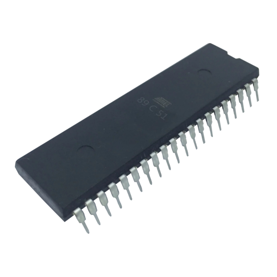
Advertisement
Quick Links
Designing Boards with Atmel AT89C51,
AT89C52, AT89C1051, and AT89C2051 for
Writing Flash at In-Circuit Test
Recent improvements in chips and
testers have made it possible for the
tester to begin taking over the role tradi-
tionally assigned to the PROM program-
mer. Instead of having a PROM pro-
grammer write nonvolatile memories
before assembling the board, the in-cir-
cuit tester writes them during in-circuit
testing operations. Many Teradyne Z18-
series testers are now in use loading
code into nonvolatile memories, micro-
controllers and in-circuit programmable
logic devices. The purpose of this note is
to explain how the Z18 approaches the
writing task for Atmel AT89C series IC's,
so that designers of boards using these
chips can get the best results.
To write the flash memories embedded
in the Atmel AT89C series chips, the
Z18-family tester must be equipped with
the Digital Function Processor (DFP)
option.
The Atmel Technical Brief titled "Inte-
grated Flash Memory Gives AT89C51
In-System Reprogrammability" describes
two approaches, one parallel and the
other serial. The Teradyne Z18XX tester
with DFP can work with either, but this
paper will only discuss the parallel
approach. The serial method looks sim-
pler at first glance, but you must con-
sider that the AT89C series which serves
as the serial interface must also have its
code loaded by the tester. At some point,
therefore, the parallel method must be
used.
The Parallel Approach
There are some simple, yet important,
des ign co nstr ai nts for the par al lel
approach, as pointed out in the Atmel
Technical Brief. If these constraints have
not been observed during board design,
it may not be possible for a tester to write
the chip's flash memory, and the chip will
have to be written with a PROM pro-
grammer before being installed on the
board. There are four main ways to inter-
fere with the tester's attempts to write
the flash memory. The four Don'ts:
• Don't tie needed input pins to V
ground;
• Don't tie needed input pins to outputs
of other IC's;
• Don't tie supervoltage input pins to
components that won't tolerate the
voltage;
• Don't tie output pins needed for
checking the write operation to other
IC outputs.
It is always possible to design a board
within the constraints described here.
The Atmel Technical Brief points out
specific pins that need attention, and
explains how to work with these pins to
insure in-circuit writability. These are dis-
cussed in detail below.
EA/V
(AT89C51/52) or
PP
RST/V
(AT89C1051/2051)
PP
The tester will take this pin high during
flash memory write and erase opera-
tions. EA/V
(AT89C51/52) or RST/V
PP
(AT89C1051/2051) will generally be
fixed either high or low when the board is
carrying out its normal mission, depend-
ing on whether the application uses
external addressing or runs entirely on
its internal memory. There are four
things to remember about this pin.
1. In certain parts of the Atmel doc-
umentation, Atmel recommends
Designing
Boards with
Atmel Flash
Microcontrollers
Application
or
CC
Note
Microcontroller
PP
Rev. 0534B-A–12/97
5-111
Advertisement

Summary of Contents for Atmel AT89C51
- Page 1 There are some simple, yet important, des ign co nstr ai nts for the par al lel 1. In certain parts of the Atmel doc- Rev. 0534B-A–12/97 approach, as pointed out in the Atmel umentation, Atmel recommends Technical Brief.
-
Page 2: Data Ports
Note: For the AT89C1051/2051 the tester disable P1 input signals originating on the board during flash mem- Data Ports (P0, P1, P2, P3 for AT89C51/52 and ory writing and erasing. P1, P3 for AT89C1051/2051) 3. If any other chips have their outputs connected to... - Page 3 Two DR2p cards (that is, one from the base unit and one expansion kit) are required for one AT89C51/52 chip, and one DR2p card is required for each AT89C1051/2051 chip on the board. Using the Atmel AT89C51 or AT89C52 3.
- Page 4 208 (DR2p 0 - group C) Input from DFP to DUT Clock The AT89C51/52 Clock must be running during flash writ- ing. Most boards have clock circuits which will be normally running while the board is on its fixture with power applied.
- Page 5 Microcontroller Using the Atmel AT89C1051 or backdrive, and will also prevent the other chip from interfering with the tester’s signals during the flash AT89C2051 memory writing or erasing processes. Pay special XTAL1 attention to intermittent signal sources such as The tester will apply logic level signals to this pin during interrupts or external or external timing inputs that flash memory write and erase operations.


Need help?
Do you have a question about the AT89C51 and is the answer not in the manual?
Questions and answers