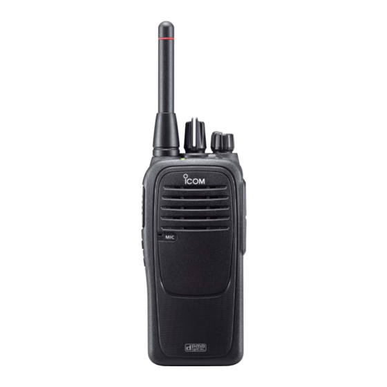
Icom IC-F29DR Service Manual
Dpmr446/pmr446 transceiver
Hide thumbs
Also See for IC-F29DR:
- Operating instructions manual (23 pages) ,
- Instruction manual (64 pages)
Advertisement
Quick Links
Advertisement

Related Manuals for Icom IC-F29DR


Summary of Contents for Icom IC-F29DR
- Page 1 dPMR446/PMR446 TRANSCEIVER S-15207XZ-C1 August 2015...
- Page 2 8. READ the instructions of the test equipment thoroughly before connecting it to the transceiver. Icom, Icom Inc. and the Icom logo are registered trademarks of Icom Incorporated (Japan) in Japan, the United States, the United Kingdom, Germany, France, Spain, Russia, Australia, New Zealand, and/or other countries.
-
Page 3: Table Of Contents
TABLE OF CONTENTS SECTION SPECIFICATIONS SECTION INSIDE VIEWS SECTION DISASSEMBLY INSTRUCTION SECTION CIRCUIT DESCRIPITON RECEIVER CIRCUITS ..................4-1 TRANSMITTER CIRCUITS ................4-2 FREQUENCY SYNTHESIZER CIRCUITS ............4-3 VOLTAGE BLOCK DIAGRAM ................4-3 SECTION PARTS LIST SECTION MECHANICAL PARTS SECTION BOARD LAYOUTS SECTION BLOCK DIAGRAM SECTION... -
Page 4: Specifications
50 (Nominal) • Antenna impedance: • Operating temperature range: –25˚C to +55˚C • Power supply: Only specified Icom's battery packs (7.5 V DC, negative ground) • Current drain (approximately): Receiving 0.11 A (Digital mode, stand-by) 0.4 A (maximum audio, internal speaker) Transmitting 0.5 A (at 0.5 W ERP) - Page 5 M RECEIVER • Sensitivity: Analog (Narrow) 26.5 dBµV/m (at 20 dB SINAD) Digital –8 dBµV emf typical (at 5% BER) • Squelch sensitivity (threshold): 26.5 dBµV/m • Intermediate frequency: 46.35 MHz 450 kHz • Intermodulation: Analog (Narrow) 86.29 dBµV/m Digital 71 dBµV (EMF) minimum, 74 dBµV (EMF) typical •...
-
Page 6: Section 2 Inside Views
SECTION 2. INSIDE VIEWS • MAIN UNIT LED DRIVER (TOP VIEW) (Q42) LED DRIVER (Q41) AF POWER AMP (IC6) +5 V REGULATOR (IC4) APC AMP (IC3) 7.2 V LINE SW (Q33) 1st IF FILTER (For analog mode) (FI2) EEPROM (IC12) LOGIC LEVEL CONVERTER (IC15) (Q39) - Page 7 • MAIN UNIT (BOTTOM VIEW) AF POWER AMP DRIVER (Q35) RF AMP (Q22) POWER AMP (Q23) 1st IF FILTER (For analog mode) (FI1) DRIVE AMP (Q21) PRE-DRIVE AMP (Q18) IF IC (IC2) LOCK VOLTAGE SELECT SW (IC1) AF AMP “S5V” LINE SW (IC8) (Q2) “R5V”...
-
Page 8: Section 3 Disassembly Instruction
2) Remove 2 screws and jack panel. SPEAKER CABLE Remove with; “ICOM Driver (K)” (8960000110) 2. REMOVING THE MAIN UNIT 1) Unsolder total of 13 points as shown. 3) Remove 2 screws from the bottom of the CHASSIS. UNSOLDER... -
Page 9: Receiver Circuits
SECTION 4. CIRCUIT DESCRIPTION 4-1 RECEIVER CIRCUITS 2ND IF AND DEMODULATOR CIRCUITS RF CIRCUITS The signal from the 1st IF circuits is applied to the IF IC (IC2) The RX signal from the antenna is passed through the LPF which contains the 2nd IF mixer, 2nd IF AMP, FM detector, (L29, L32, L34, C191, C194, C199, C202 and C205), an- squelch circuit and AF AMP in its package. -
Page 10: Transmitter Circuits
TX AMPLIFIERS 4-2 TRANSMITTER CIRCUITS The buffer amplified signal from the LO SW (D12) is se- TX AF CIRCUITS (MAIN UNIT) quentially amplifi ed by the pre-drive AMP (Q18), drive AMP The audio signal from the internal or external microphone (Q21), and power AMP (Q23), to obtain TX power. -
Page 11: Frequency Synthesizer Circuits
4-3 FREQUENCY SYNTHESIZER CIRCUITS 4-4 VOLTAGE DIAGRAMS Voltage from the power supply is routed throughout the The RX VCO is composed of Q6, D7 and D10. The VCO out- transceiver, through regulators and switches. put signal is buffer-amplified by two buffers (Q11 and Q16) and applied to the 1st IF mixer, through the LO SW (D13) Q33,26, and the LPF (L17, C126 and C131). - Page 12 SECTION 5. PARTS LIST [MAIN UNIT] [MAIN UNIT] PARTS PARTS DESCRIPTION DESCRIPTION LOCATION LOCATION 1110008770 S.IC AK2400-L 52.4/15.6 6050013800 S.XTA CR-980 14.7456 MHz<SKD> 12.8/38.3 1110002751 S.IC TA75S01F(TE85RF) 84.1/34.0 6050013980 S.XTA CR-997 DSA221SCM 1180003320 S.REG NJM2830U1-05-TE1-#ZZZB 85.9/23.2 12.288 MHz 11.5/8.8 1110007920 S.IC SC-1445-E2 30.5/9.3 1110007610 S.IC...
- Page 13 [MAIN UNIT] [MAIN UNIT] PARTS PARTS DESCRIPTION DESCRIPTION LOCATION LOCATION 7030008300 S.RES ERJ2GEJ 184 X (180K) 51.2/10.4 R153 7030005220 S.RES ERJ2GEJ 223 X (22K) 28.6/19.4 7030005080 S.RES ERJ2GEJ 823 X (82K) 38.9/35.6 R154 7030005160 S.RES ERJ2GEJ 105 X (1M) 24.5/24.8 7030005090 S.RES ERJ2GEJ 104 X (100K) 47.0/15.5 R155...
- Page 14 [MAIN UNIT] [MAIN UNIT] PARTS PARTS DESCRIPTION DESCRIPTION LOCATION LOCATION R279 7030005050 S.RES ERJ2GEJ 103 X (10K) 14.5/29.6 4030017460 S.CER C1005 JB 1H 102K-T 65.6/9.7 R280 7410001130 S.ARR EXB28V102JX 24.1/25.7 4030016930 S.CER C1005 JB 1A 104K-T 67.0/12.9 R281 7030005160 S.RES ERJ2GEJ 105 X (1M) 15.6/37.8 4030016930 S.CER C1005 JB 1A 104K-T 63.6/11.3...
- Page 15 [MAIN UNIT] [MAIN UNIT] PARTS PARTS DESCRIPTION DESCRIPTION LOCATION LOCATION C135 4030017580 S.CER C1005 CH 1H 060C-T [#01] B 76.3/12.5 C248 4030016930 S.CER C1005 JB 1A 104K-T 35.4/13.4 4030017380 S.CER C1005 CH 1H 050B-T [#02] C249 4030020000 S.CER C1005 JB 1A 105K-T 29.7/14.7 4030017380 S.CER C1005 CH 1H 050B-T [#03]...
- Page 16 [MAIN UNIT] PARTS DESCRIPTION LOCATION C374 4030016790 S.CER C1005 JB 1E 103K-T 20.2/12.3 C375 4030016790 S.CER C1005 JB 1E 103K-T 16.8/17.8 C376 4030016790 S.CER C1005 JB 1E 103K-T 16.0/10.8 C377 4030017460 S.CER C1005 JB 1H 102K-T 17.2/10.3 C378 4030020000 S.CER C1005 JB 1A 105K-T 23.6/17.4 C379 4030018910 S.CER C1608 JB 0J 475K-T...
- Page 17 SECTION 6. MECHANICAL PARTS [CHASSIS PARTS] [ACCESSORIES] ORDER ORDER DESCRIPTION QTY. DESCRIPTION QTY. 3310004750 3621 ANT <EIK> (Optional) BP-280 (Optional) BC-123SE [#21] 2510001980 036D01204 (Optional) BC-123SUK [#22] (Optional) BC-213 8010023041 3621 CHASSIS-1 8210031290 3621 FRONT PANEL (B) ASSEMBLYA-4 (Optional) MB-133 (including W1, SP1, MP3, 4, 5, 9, 10, 23, 28, 32, 33, MP42, 47, 48, 53) 8210029620 3621 3621 PTT PANEL...
- Page 18 MP55(CHASSIS) MP34(CHASSIS) Remove with; (6910018220) (8830001701) “ICOM Driver (AG)” (8960000560) MP11(CHASSIS) EP2(CHASSIS) (8930089300) (3310004750) MP30(CHASSIS) ANT UNIT (8930090130) MP16(CHASSIS) MP44(CHASSIS) S1(MAIN) (8930084870) (8810009511) (2250000900) MP40(CHASSIS)×2 (8810010850) R141(MAIN) (7210003700) MP7(CHASSIS) (8930089240) EP7(MAIN) MAIN UNIT (6910024510) MP39(CHASSIS) MP26(CHASSIS) MP45(CHASSIS)×2 (8930085330) (8810008761) (8930089270)
- Page 19 SECTION 7 BOARD LAYOUTS • MAIN UNIT B-8270A (TOP VIEW) [PTT] B-8270A C223 C339 C340 C164 R105 C211 C175 R310 R113 C325 R116 R119 R276 R238 R259 C312 R311 IC12 C316 C335 C311 R279 R204 R208 R217 R218 C233 R207 C317 R160 R161...
- Page 20 • MAIN UNIT B-8270A (BOTTOM VIEW) R144 R137 C338 C214 C210 R308 C120 C336 R285 C128 EP14 C149 R281 C154 R278 C299 C179 R286 C134 C104 C123 R262 R226 C151 R245 C305 C205 C306 C206 C111 C125 C138 C303 C119 C204 C310 C199...
- Page 21 SECTION 8. BLOCK DIAGRAM Q 8 , D 1 1 MAIN UNIT S 5 V 4 4 6 . 0 0 6 2 5 0 - R I P P L E V C O V 4 4 6 . 1 9 6 8 7 5 MHz F I L A N T S 5 V...
- Page 22 SECTION 9. VOLTAGE DIAGRAM • MAIN UNIT (1/3) TX 4.9 V DC_SW RX 0.0 V 2SA1586 MAIN UNIT (2/3) 2SC4116 VCOV KTA2015 Ripple DC_SW 4.9 V VCOV Filter 7.5 V 4.2 V 3.3V LDTC114YE 3.3V LDTC114YE MMZ1005S800CT 100k 100k 3.3k MMZ1005Y102CT VCON VCO_TX...
- Page 23 • MAIN UNIT (2/3) 3.3V 3.3V T/R_LIGHT TX 3.3 V R217 RLED R196 RX 0.0 V DC_SW LDTA114YE EXTV TX 0.0 V R218 TLED CPUV RX 3.3 V C241 C245 CP10 MMZ1005A152ET LDTA114YE CL-165HR EP12 R310 100k C242 LDTC114YE CP11 R150 C246 0.015...
- Page 24 • MAIN UNIT (3/3) EP14 3.3 V NFM18PC104R1C3 MMZ1005A152ET C342 EP18 MMZ1005A152ET EP19 3.3V_D CPUV MMZ1005A152ET D-GND 1.6V_D A-GND 1.6 V 3.3 V J-TAG 3.3V_D AGND EP20 R346 OUT_S MMZ1005F560C EP21 R347 TRST MMZ1005F560C EMU0 DC-DC EMU1 1.6V BDX0 DVDD BFSX0 DVDD BCLKX0...
- Page 25 Highway 17A Delta, B.C., V4K 5B8, Canada : http://www.icomspain.com Phone : +1 (604) 952-4266 Fax : +1 (604) 952-0090 E-mail : icom@icomspain.com : http://www.icomcanada.com E-mail : info@icomcanada.com Blacksole House, Altira Park, Herne Bay, Kent CT6 6GZ, UK Phone : +44 (0) 1227 741741...
- Page 26 S-15207XZ-C1 1-1-32, Kamiminami, Hirano-ku, Osaka 547-0003, Japan © 2015 Icom Inc.
Need help?
Do you have a question about the IC-F29DR and is the answer not in the manual?
Questions and answers