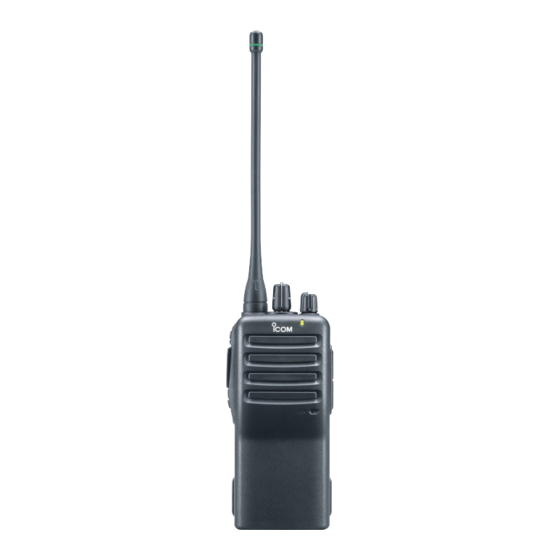
Icom IC-F24 Service Manual
Uhf transceivers
Hide thumbs
Also See for IC-F24:
- Instruction manual (21 pages) ,
- Instruction manual (48 pages) ,
- Servise manual (8 pages)
Table of Contents
Advertisement
Advertisement
Table of Contents

Subscribe to Our Youtube Channel
Related Manuals for Icom IC-F24


Summary of Contents for Icom IC-F24
- Page 1 SERVICE MANUAL UHF TRANSCEIVERS...
- Page 2 8. READ the instructions of test equipment thoroughly before connecting equipment to the transceiver. Icom, Icom Inc. and are registered trademarks of Icom Incorporated (Japan) in the United States, the United Kingdom, Germany, France, Spain, Russia and/or other countries.
-
Page 3: Table Of Contents
TABLE OF CONTENTS SECTION SPECIFICATIONS SECTION INSIDE VIEWS SECTION DISASSEMBLY INSTRUCTIONS SECTION CIRCUIT DESCRIPITON RECEIVER CIRCUITS ............4-1 TRANSMITTER CIRCUITS . -
Page 4: Section 1 Specifications
16K0F3E (25.0 kHz) [EUR] 14K0F3E (20.0 kHz) 8K50F3E (12.5 kHz) • Number of conventional channels : 2 ch (IC-F24S/F25S), 16 ch (IC-F24/F25) : 50 Ω (nominal) • Antenna impedance • Operating temperature range : –30˚C to +60˚C (–22˚F to +140˚F) [USA], [GEN] –25˚C to +55˚C... -
Page 5: Section 2 Inside Views
SECTION 2 INSIDE VIEWS • MAIN UNIT TOP VIEW BOTTOM VIEW Pre-drive (Q5: 2SC3356) Power amplifier (Q7: RD07MVS1) Drive amplifier (Q8: RD01MUS1) AF amplifier +5 Regulator (IC12: TA7368F) (IC9: NJM2870) S5 Regulator Q23: 2SB1132 Q24: XP6501 Q25: UNR9113J T5 Regulator Crystal filter (Q21: 2SA1577) (FI1: FL-335) -
Page 6: Section 3 Disassembly Instructions
Chassis unit *: IC-F24/F25 only • • REMOVING THE MAIN UNIT (IC-F24/F25) REMOVING THE MAIN UNIT (IC-F24S/F25S) 1 Unscrew 2 nuts F, and remove the top plate G. 1 Remove the switch connector O. 2 Unsolder 1 point H, and remove the earth plate. -
Page 7: Receiver Circuits
SECTION 4 CIRCUIT DESCRIPTION The RF signals from the bandpass filter are mixed with the 4-1 RECEIVER CIRCUITS 1st LO signals, where come from the RX VCO circuit via 4-1-1 ANTENNA SWITCHING CIRCUIT the BPF (L12, L38, C49, C304, C305), at the 1st mixer cir- The antenna switching circuit functions as a low-pass filter cuit (Q3) to produce a 46.35 MHz 1st IF signal. -
Page 8: Transmitter Circuits
4-1-5 AF AMPLIFIER CIRCUIT • CTCSS AND DTCS The tone squelch circuit detects tone signals and opens the The AF amplifier circuit amplifies the demodulated AF sig- squelch only when the receiving signal contains matched nals to drive a speaker. subaudible tone (CTCSS or DTCS). - Page 9 4-2-4 APC CIRCUITS 4-2-2 MODULATION CIRCUITS The bias current of the drive (Q8) and power (Q7) amplifiers The modulation circuit modulates the VCO oscillating signal are controlled by the APC circuit. (RF signal) using the audio signals from the microphone. The AF signals from the D/A converter (IC8, pin 3) change The APC circuit (IC2, D1, D30) protects drive and power the reactance of varactor diode (D18) to modulate the oscil-...
-
Page 10: Pll Circuits
4-3-2 VCO CIRCUITS 4-3 PLL CIRCUITS The VCO circuit contains a separate RX VCO (Q14, D16, 4-3-1 PLL CIRCUIT D22) and TX VCO (Q13, D17, D21). The oscillated signal A PLL circuit provides stable oscillation for the transmit fre- is amplified at the buffer amplifiers (Q10, Q12) and is then quency and the receive 1st LO frequency. -
Page 11: Other Circuits
4-6 PORT ALLOCATION 4-4 OTHER CIRCUITS LED CONTROL CIRCUITS 4-6-1 D/A CONVERTER IC (IC8) The LED control circuit is composed of the CPU (IC13), Port LED driver (Q32) and LED (DS1). Description number name The CPU outputs “RLED” and “TLED” signals from the pins Outputs the modulation balance level 42 and 43. - Page 12 4-6-2 CPU (IC13) Port Port Description Description number name number name Input port for the transceiver’s RLED Outputs receiving LED control signal. TEMP internal temperature detecting Outputs transmitting LED control signal. TLED signal. Input port for the detect signal BATV for connecting battery pack’s OPT3 voltage.
-
Page 13: Section 5 Adjustment Procedures
SECTION 5 ADJUSTMENT PROCEDURES 5-1 PREPARATION When adjusting IC-F24/F25/S, the optional CS-F14 ADJ (Rev. 1.0 or later), JIG cable (see the illust ADJUSTMENT SOFTWARE below) and OPC-478 (RS-232 type) or OPC-478U (USB type) are required. CLONING CABLE REQUIRED TEST EQUIPMENTS... -
Page 14: Configuration Lists For Adjustments
5-2 CONFIGULATION LIST FOR ADJUSTMENTS - IC-F24/F25 - [US2]=USA-02, [GE2]=GEN-02, [EU2]=EUR-02, [US3]=USA-03, [GE3]=GEN-03 FREQUENCY (MHz) FREQUENCY (MHz) SETTING CONDITION SETTING CONDITION [US2], [EU2], [US2], [EU2], [US3], [GE3] [US3], [GE3] [GE2] [GE2] Set TX power to Low1. Set DTCS code to 007. - Page 15 SINAD meter JIG cable To [SP] (see page 5-1) Speaker (8 Ω) IC-F24/F25/S (JIG CABLE ( SP + ) (SP − ) (GND) 3-conductor 3.5(d) mm plug OPC-478/U JIG cable To IC-F24/F25/S [SP] jack (CLONE) 5 - 3...
- Page 16 (PC SCREEN EXAMPLE NOTE: The above screen is an example. Each transceiver has its own specific values for each setting. 5 - 4...
-
Page 17: Software Adjustments
5-3 SOFTWARE ADJUSTMENTS (TRANSMITTING) Select the operation using [↑] / [↓] keys, then set specified value using [←] / [→] keys on the connected computer keyboard. MEASUREMENT ADJUSTMENT ADJUSTMENT CONDITION VALUE UNIT LOCATION PLL LOCK • Operating CH : CH2 (*CH1) "... - Page 18 5-3 SOFTWARE ADJUSTMENTS (RECEIVING) • Select an operation using [↑] / [↓] keys, then set specified value using [←] / [→] keys on the connected computer keyboard. MEASUREMENT ADJUSTMENT ADJUSTMENT CONDITION VALUE UNIT LOCATION CTCSS/DTCS 1 • Operating CH : CH10 (*CH1) Connect the FM deviation ±0.68 kHz DEVIATION...
-
Page 19: Main Unit
SECTION 6 PARTS LIST [MAIN UNIT] [MAIN UNIT] ORDER ORDER DESCRIPTION DESCRIPTION LOCATION LOCATION 1110003200 S.IC TA31136FN (EL) 51.8/19 6070000190 S.DCR CDBCB450KCAY24-R0 54.4/20 1130008560 S.IC TC75S51F (TE85L) 68.9/21 6050011940 S.XTL CR-783 (15.3 MHz) 36.9/28.9 1140005990 S.IC MB15A02PFV1-G-BND-ER 38.3/35.7 6050011720 S.XTL CR-764 (19.6608 MHz) 12/5.9 1110005340... - Page 20 [MAIN UNIT] [MAIN UNIT] ORDER ORDER DESCRIPTION DESCRIPTION LOCATION LOCATION 7030005110 S.RES ERJ2GEJ 224 X (220 kΩ) 72.2/38.9 R123 7030008400 S.RES ERJ2GEJ 182 X (1.8 kΩ) 75.2/37.7 7030005050 S.RES ERJ2GEJ 103 X (10 kΩ) 69.2/38.9 R124 7030005170 S.RES ERJ2GEJ 474 X (470 kΩ) 72.7/40.4 7030005110 S.RES...
- Page 21 [MAIN UNIT] [MAIN UNIT] ORDER ORDER DESCRIPTION DESCRIPTION LOCATION LOCATION R235 7030005090 S.RES ERJ2GEJ 104 X (100 kΩ) 20.3/4.2 4030017460 S.CER ECJ0EB1E102K 75.8/39.9 4030017460 S.CER ECJ0EB1E102K 77.1/38.7 R236 7030005230 S.RES ERJ2GEJ 334 X (330 kΩ) 23.3/5.2 R237 7030005050 S.RES ERJ2GEJ 103 X (10 kΩ) 21.1/39.1 4030017420 S.CER...
- Page 22 [MAIN UNIT] [MAIN UNIT] ORDER ORDER DESCRIPTION DESCRIPTION LOCATION LOCATION C114 4030017360 S.CER ECJ0EC1H030B 51.9/36.5 C208 4030017590 S.CER ECJ0EC1H070C 54.2/42.3 C209 4030017460 S.CER ECJ0EB1E102K 54.2/43.3 [US3], [GE3], [US3S], [GE3S] 4030017580 S.CER ECJ0EC1H060C [Others] C211 4030018910 S.CER C1608 JB 0J 475K-T 36.1/21.9 C115 4030017570...
-
Page 23: Ant Unit
[MAIN UNIT] ORDER DESCRIPTION LOCATION C324 4030017420 S.CER ECJ0EC1H470J 85/13.7 C325 4550006250 S.TAN TEESVA 1A 106M8L 90.6/17.2 C326 4510006940 S.ELE EEVFC0J101P 87.8/8.9 C333 4030017420 S.CER ECJ0EC1H470J 76.8/39.9 C335 4030018860 S.CER ECJ0EB0J105K 57.2/21.1 C339 4030016930 S.CER ECJ0EB1A104K 5.9/17.2 C340 4030016930 S.CER ECJ0EB1A104K 9.3/12.5 C341... -
Page 24: Cabinet Parts
SECTION 7 MECHANICAL PARTS AND DISASSEMBLY 7-1 CABINET PARTS [MAIN UNIT] [ACCESSORIES] REF. ORDER. NO. DESCRIPTION QTY. REF. ORDER. NO. DESCRIPTION QTY. 6450001680 HSJ1122010010 3310002311 FA-SC25U-1 [US2], [US2S], [EU2] 6450002250 HSJ1456-010320 [EU2S], [GE2], [GE2S] 3310002291 FA-SC57U-1 [US3], [US3S] R226 7210003061 TP76N00N-15F-A103-2251A [GE3], [GE3S] 0800007541... - Page 25 W1 ( C ) IC-F24S/F25S MP28 ( C ) MP21 ( C ) MP34 ( C ) MP22 ( C ) 31 (1 1.7 ( 1.7 ( *: IC-F24/F25 only 7/32 1/16 1/16 17.8 ( 38 (1 4.8 ( 53 (2 11/16...
- Page 26 SECTION 8 SEMI-CONDUCTOR INFORMATION • TRANSISTORS AND FETs 2SA2048TL R 2SB1132 R 2SC3356 R25 2SC4116 BL 2SC4215 O (Symbol: UL) (Symbol: BARB) (Symbol: R25) (Symbol: LL) (Symbol: QO) 2SC4226 R25 2SC5107 O 2SK1829 2SK3019 2SK880 Y (Symbol: BR) (Symbol: MFO) (Symbol: K1) (Symbol: KN) (Symbol: XY)
- Page 27 SECTION 9 BOARD LAYOUTS 9-1 MAIN UNIT • TOP VIEW Horizontal C148 R169 C259 C152 C153 R155 C151 R124 C277 R168 C278 R181 C285 R180 R156 C261 R117 R118 R172 R237 C284 R182 C260 R157 C154 C149 C155 C116 C126 R123 C173 C117...
- Page 28 • BOTTOM VIEW R107 C209 R101 C141 C208 C143 C109 C206 C305 C287 C304 C130 R183 R100 C186 C300 C288 C105 C103 OPV1 C111 OPV2 DAST C160 C177 CIRQ OPT3 OPT2 CP10 OPT1 DISC SIGO R113 C289 CP11 C203 BUSY BEEPO AFONO C144...
-
Page 29: Block Diagram
SECTION 10 BLOCK DIAGRAM 400-520 MHz Q18: Q17: Q15: XP1214 2SK880 2SC4116 Q16: UNR9213J Q14: 2SC4226 LVIN RIPPLE D16: HVC350B BUFF D22: HVC350B RX VCO CR-783 Q12: Q10: D14, D15: D2: 1SV307 RD07MVS1 15.3 MHz 2SC5107 2SC5107 MA2S077 2SC5107 2SC3356 RD01MUS1 D5: MA2S077 LOOP... -
Page 30: Voltage Diagram
SECTION 11 VOLTAGE DIAGRAM 11-1 MAIN UNIT ANT BOARD 2.5 P 1.5 P T: 3.3 T: 1.7 VCO5 R: 0.0 R: 0.0 C: 4.2 C: 4.9 17.5 nH RX VCO T: 7.1 6.8 k C: 4.7 C: 3.9 C211 T: 3.9 2SC4116 BL R: 7.2 14 nH... - Page 31 E-mail : info@icomcanada.com Unit 9, Sea St., Herne Bay, Kent, CT6 8LD, U.K. Phone : +44 (01227) 741741 Fax : +44 (01227) 741742 Icom (Australia) Pty. Ltd. : http://www.icomuk.co.uk E-mail : info@icomuk.co.uk A.B.N. 88 006 092 575 290-294 Albert Street, Brunswick, Victoria, 3056, Australia Icom France S.a...
- Page 32 S-14116IZ-C1 1-1-32, Kamiminami, Hirano-ku, Osaka, 547-0003, Japan © 2004 Icom Inc.
Need help?
Do you have a question about the IC-F24 and is the answer not in the manual?
Questions and answers