Table of Contents
Advertisement
Quick Links
Advertisement
Table of Contents
Troubleshooting

Related Manuals for Samsung SPR-5200


Summary of Contents for Samsung SPR-5200
- Page 1 SAMSUNG SPR-5200 MODEL SERVICE MANUAL...
-
Page 2: Table Of Contents
CONTENTS 1. Product Specification 3. Exploded View & Parts List 3-1 SP-R5200 HANDSET P/L 3-2 SP-R5200 HANDSET Exploded View 2. Operations & Installation 3-3 SP-R5200 BASE P/L 2-1 Checking Parts 3-4 SP-R5200 BASE Exploded View 2-2 Control Locations 3-5 SP-R5200 CHARGER P/L 2-3 Connecting Lines 3-6 SP-R5200 CHARGER Exploded View 2-4 Installing Handset Batteries... -
Page 4: Product Specification
1. Product Specification Item Description Frequency Range 1881.792MHz~1897.344MHz Channels 120 Duplex Channels Channel Separation 1,728MHz Carrier Power ²250mW (24dBm) Modulation GFSK Frequency Stability ² ± 50kHz Standby Mode : 120hr Operation Time Talk Mode : 12hr Charging time : 15hr Normal : 15ûC~35ûC Ambient Temperature Extreme : 0ûC~40ûC... -
Page 5: Operations & Installation
2. Operations & Installstion 2-1 Checking Parts Once you have unpacked your phone, check to make sure that you have all the parts shown below. If any piece is missing or broken, please call your dealer. Base Handset Adapter Line Cord Two AA Batteries Service Manual (Rechargeable Ni-Cd batteries) -
Page 6: Control Locations
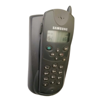
2-2 Control Locations 2-2-1 Handset Antenna Earpiece LCD window button Makes, answers, or ends a call. INT button Activates intercom communications. button Scrolls through menus. Also adjusts volume. C/R button Clears characters from the display. Also performs a switch-hook operation such as call waiting. PQRS WXYZ button... - Page 7 2-2-2 Base Paging button Allows you to page the handset. Also used to register a new handset with the base. Line lamp Blinks when a call comes in and lights steadily when a call is in progress. Base Bottom DC POWER socket Phone Line socket Operations &...
-
Page 8: Connecting Lines
2-3 Connecting Lines 1. Connect one end of the telephone line cord to the phone line socket on the bottom of the base unit, and the other end to a standard phone wall jack. 2. Connect the modular end of the power adapter to the DC power socket on the bottom of the base unit, and the other end to a standard AC wall outlet. -
Page 9: Installing Handset Batteries
2-4 Installing Handset Batteries The handset uses the two AA size rechargeable Ni-MH or Ni-Cd batteries supplied. 1. Slide the battery cover in the direction of the arrow, then lift it off. 2. Remove old batteries if any, then insert new batteries observing correct polarity ( + , - ). Reversing the orientation may damage the handset. - Page 10 3. Replace the battery cover. Make sure that the cover is hooked in place. 4. Slide the cover up until it snaps shut. Notes: ¥ The batteries need to be replaced if they do not recover their full storage capacity after recharging. ¥...
-
Page 11: Charging The Handset
2-5 Charging the Handset Before initial operation, you should fully charge the handset for more than 15 hours. To charge the handset, simply place it on the base unit. The handset can be charged either face up or face down. Result: When the handset batteries are charging, the handset automatically turns on and the battery icon on the left corner of the display is scrolling. -
Page 12: Using The Handset Carrying Clip
2-6 Using the Handset Carrying Clip The supplied handset carrying clip allows you to conveniently carry the handset with you. It clips easily to your belt, waist band, or shirt pocket. To Attach the Carrying Clip Attach the carrying clip to the back of the handset. The carrying clip fits into the grooves on the back of the handset as shown. -
Page 13: Turning The Handset On/Off
2-7 Turning the Handset On/Off When you place the handset in the base unit to charge it, the handset automatically turns on. To turn the handset on or off in Standby mode, follow these steps: 1. To turn on the handset when the display is off, press button. -
Page 14: Lcd Window Icon Descriptions
2-8 LCD Window Icon Descriptions Battery status icon Line/Intercom/icon In range icon Handset key lock icon Memory icon Volume level icon 2-9 Choosing Dial Mode In order to provide compatibility with most telephone systems, your phone can be set to either pulse-dialling (same as rotary), or tone dialling (DTMF). -
Page 15: Making A Call
2-10 Making a Call 1. Pick up the handset and press button. You hear a dial tone. 2. Dial the desired number by using the number keypad. Note: You can store telephone numbers into one-digit memory cells (0-9) and dial the numbers using the assigned memory cell number. -
Page 16: Camp On Busy
2-11 Camp On Busy (This feature is available only when you have more than one handset) This feature allows your handset to wait for connection to the telephone line currently engaged by another handset. Your handset rings when the telephone line becomes free. 1. -
Page 17: Receiving A Call
2-12 Receiving a Call 1. When an external call comes in, the phone rings. Result: The icon on the display blinks, and the green lamp on the back of the handset flashes. 2. To answer the call, press button. If the handset is on the base unit, simply lift it up. You do not need to press button. -
Page 18: Caller Id Display
2-13 Caller ID Display Caller ID is a feature available on your phone which helps you to know who is calling by displaying the callerÕs number when the phone rings. Contact your service provider to activate this feature. This icon blinks when the phone rings. -
Page 19: Out Of Range Indication
2-14 Out of Range Indication If the handset is too far from the base unit, the handset cannot properly engage the telephone line, and the icon blinks in the LCD window. This icon blinks when the handset is out of range in the standby mode. -
Page 20: Adjusting Voice Volume
2-16 Adjusting Voice Volume During calls, button affects the ear piece volume. You can adjust the volume from level 1 to 5 , and it is preset to level 3. The voice volume is displayed as bars on the upper right corner of the LCD window. The more bars you see, the louder the volume is. -
Page 21: Adjusting Ring Volume
2-18 Adjusting Ring Volume 1. Press button repeatedly until appears in the display. 2. Press button to access the menu. Result: The current ring level is displayed. You can hear the volume loudness. 3. Press button to choose the volume level you want. Result: You can adjust the volume from level 1 to 3. -
Page 22: Memory Dialing
2-20 Memory Dialing 2-20-1 To Store (or Edit) Numbers In Memory You can store the most frequently used phone numbers into one-digit memory cells (0-9). 1. Press button repeatedly until appears in the display. 2. Press button. Result: The first memory cell (0) containing a phone number, if already stored, is displayed. 3. -
Page 23: Call Log
4. Press button. Result: The number is automatically dialed. 2-20-4 To Erase All Numbers In Memory If you reset the handset, all numbers stored in memory are erased. Refer to ÔResetÕ on page 2-32. 2-21 Call Log When you receive a call, the callerÕs phone number is shown on your phoneÕs display if it is available from the network on which the call was made. -
Page 24: Last Number Redial
2-22 Last Number Redial Your phone allows you to call the most recently dialed numbers again. The phone stores the last 10 numbers you called. 2-22-1 To View and Dial the Numbers 1. Press button. Result: The LCD window displays the last number you dialed. 2. -
Page 25: Call Time Display On/Off
2-23 Call Time Display On/Off If you turn the feature on, the handset automatically times the duration of calls. The handset displays the call duration both during your call and also for a few seconds after your call is completed. The feature is preset to ÔOFFÕ. -
Page 26: Base Number Display On/Off
2-25 Base Number Display On/Off This feature allows the phone to display the base number currently in use while in Standby mode. The feature is preset to ÔOnÕ at factory. 1. Press button until appears in the display. 2. Press button. -
Page 27: Setting Ring Delay Time
2-27 Setting Ring Delay Time If you activate the ring delay time, your handset will not ring for the specified delay time while other handsets are ringing. If you wish, you can answer the call within the delay time on your handset. 1. -
Page 28: Changing Pin (Personal Identification Number)
2-29 Changing PIN (Personal Identification Number) The PIN is required when you bar calls or register handsets to a base unit. The PIN is preset to Ô0000Õ at factory. You can change the PIN code. 1. Press button repeatedly until appears in the display. -
Page 29: Barring Calls
2-31 Barring Calls ¥ It is possible to set the phone to restrict numbers that can be dialed. The phone cannot dial a phone number beginning with the specific numbers that you specify. ¥ You can set up to 4 restricted numbers containing up to 4 digits each. ¥... -
Page 30: Reset
2-32 Reset If you reset the handset, all the user-selectable features return to the manufacturerÕs default status as shown below: ¥ Voice Volume: Level 3 ¥ Call Barring: Off ¥ Ring Level: Level 2 ¥ Ring Delay: Off ¥ Ring Type: Type 1 ¥... -
Page 31: Registering New Handset With Base
2-33 Registering New Handset with Base Up to six handsets can be registered and operated from your base unit. The system allows you to make internal calls between two handsets while a third is making an call. The supplied handset with the base unit is already registered as handset 1. Each additional handset you purchase must be registered to the base unit. - Page 32 2-33-2 To Remove a Handset Registered to the Base Unit 1. Press button repeatedly until appears in the display. 2. Press button. 3. Enter the PIN code. 4. Press button. Result: The base number appears in the display. 5. Press button.
-
Page 33: Paging
2-34 Paging You can page any registered handset from the base unit. Using this feature, you can find where the handsets are. Press the button on the center top of the base unit. Result: All handsets registered with the base will ring four times. 2-35 Intercom Between Handsets (This feature is available only when you have more than one handset) If you have multiple handsets registered with the base, two handsets can talk to each other on an internal... -
Page 34: Call Transfer
2-36 Call Transfer (This feature is available only when you have more than one handset) You can transfer a call from one handset to another. 1. During a telephone conversation, press INT button. Result: Your caller will be put on hold and will hear music. icon blinks in your display. -
Page 35: Operating With Additional Base Unit
2-37 Operating with Additional Base Unit The SP-R5200 handsets may be used with up to four base units. To use the handset with more than one base unit, you must register the handset at each base unit. Refer to ÔRegistering New Handset with BaseÕ on page 2-33. -
Page 36: Exploded View & Parts List
3. Exploded View & Parts List 3-1 SP-R5200 HANDSET P/L Location No Code No Description Specification QÕty GG72-00015A WINDOW-BOHO GG72-00007A WINDOW-LCD GG74-00002A TAPE-WINDOW GG72-00002A FRONT-COVER GG73-00004A UNIT-RUBBER GG74-00004A SPONGE-LCD GG73-00001A KEY-PAD GG72-00006A HOLDER-LCD GG73-00002A HOLDER-BUZZER GG74-10586A SPONGE-UNIT GG74-10564A SPONGE-SPEAKER GG92-00927A SUA. -
Page 37: Sp-R5200 Handset Exploded View
3-2 SP-R5200 HANDSET Exploded View Exploded View & Parts list... -
Page 38: Sp-R5200 Base P/L
3-3 SP-R5200 BASE P/L Location No Code No Description Specification QÕty GG72-00011A KEY-TOP GG61-00001A SUPPORT-SPRING GG72-00009A BASE-UPPER GG72-00012A LENS-BASE GG71-00006A SHIELD-CAN GG71-00005A SHIELE-FRAME GG71-00010A ANTENNA-WIRE GG92-00926A SUA. RF-BOARD GG71-00008A BATT-TERMINAL(A) GG71-00009A BATT-TERMINAL(B) 6002-000352 SCREW-TAPTITE TAPTITE, PWH, +, 2, M2.5X4 SUA. LOGIC-BOARD GG72-00010A BASE-LOWER GG73-00005A... -
Page 39: Sp-R5200 Base Exploded View
3-4 SP-R5200 BASE Exploded View Exploded View & Parts list... -
Page 40: Sp-R5200 Charger P/L
3-5 SP-R5200 CHARGER P/L Location No Code No Description Specification QÕty GG72-00013A CHARGER-UPPER GG71-00008A BATTERY-TERMINAL(A) GG71-00009A BATTERY-TERMINAL(B) 6002-000352 SCREW-TAPTITE TAPTITE, PWH, +, 2, M2.5X4 GG72-00014A CHARGER-LOWER GG73-00005A FOOT-RUBBER(A) 6003-001051 SCREW-TAPTITE TAPTITE, B, BH, +, M2.6X8 GG61-40101A FOOT-RUBBER GG68-00028A LABEL ID-CHARGER Exploded View &... -
Page 41: Sp-R5200 Charger Exploded View
3-6 SP-R5200 CHARGER Exploded View Exploded View & Parts list... -
Page 42: Sp-R5200 Packing P/L
3-7 SP-R5200 PACKING P/L Location No Code No Description Specification QÕty GG97-01713A H/S HOUSING ASSY GG97-01739A BASE HOUSING ASSY GG72-00005A BELT-CLIP TEL LINE GG69-10874A BOX-ADAPTOR BOX-INNER BOX-UNIT Exploded View & Parts list... -
Page 43: Sp-R5200 Packing Exploded View
3-8 SP-R5200 PACKING Exploded View Exploded View & Parts list... -
Page 44: Electrical Parts List
4. Electrical Parts List 4-1 SP-R5200 Hand Logic Parts List SEC CODE VENDOR CODE VENDOR Q’T REFERENCE DESCRIPTION 0402-001075 MBRO520LT1 MOTORORA DIODE 0404-000116 BAS40-04 SIEMENS DIODE 0406-001012 SM12 SEMTECH 1, 2 TVS-DIODE 0407-000122 1SS226 7, 8, 12, 13, 9 SW-DIODE 0501-000457 MMBT2222A 1, 3... - Page 45 SEC CODE VENDOR CODE VENDOR Q’T REFERENCE DESCRIPTION 2203-001141 GRM40X7R683K25PT MURATA 8, 9, 10, 11, 40, 41, 68 68nF, 2012 2203-005148 GRM40X7R104K25PT MURATA 12, 14, 43, 57 100nF 2402-000007 MV6.3VC220MD SAMY 22uF/6.3V(E) 2402-000107 MV6.3VC100MF SAMY 100uF/6.3V(E) 2402-001068 MV6.3VC330MD SAMY 330uF/6.3V(E) 2404-000297 TCSCS1A226KAR 22uF/10V, 6032(T)
-
Page 46: Sp-R5200 Hand Rf Parts List
4-2 SP-R5200 Hand RF Parts List SEC CODE VENDOR CODE VENDOR Q’T REFERENCE DESCRIPTION 0405-001024 1SV276 TOSHIBA 505, 506 VARACTOR DIODE 0405-001054 BB833 SIEMENS DIODE 0409-001001 BAR63-03W SIEMENS PIN DIODE 0409-001005 BAR80 SIEMENS DUAL PIN DIODE 0501-002222 BC807-25W SIEMENS 500, 501 TR-PNP 0504-001010 DTA143XUA... - Page 47 SEC CODE VENDOR CODE VENDOR Q’T REFERENCE DESCRIPTION 2203-000278 GRM36COG100D50PT MURATA 502, 504, 506, 512, 523, 525 10pF, 1005 526, 537, 540, 565, 572, 574 576, 579, 580, 581, 582, 587 598, 599, 608, 521, 516, 611 2203-000386 GRM36COG150J50PT MURATA 513, 538, 595 15pF, 1005 2203-000628...
-
Page 48: Sp-R5200 Base Logic Parts List
4-3 SP-R5200 Base Logic Parts List SEC CODE VENDOR CODE VENDOR Q’T REFERENCE DESCRIPTION 0402-000309 1SR154-400TE25 ROHM REC DIODE 0402-000318 SIZB60 PSHINDENGEN BRIDGE DIODE 0403-001047 BZX84C12 PHILIPS 1, 2 ZEMER DIODE 0403-001085 1SMB5927BT3 MOTOROLA ZEMER DIODE 0406-001012 SM12 SEMTEC ZEMER DIODE 0407-000122 1SS226 TE85R SW-DIODE... - Page 49 SEC CODE VENDOR CODE VENDOR Q’T REFERENCE DESCRIPTION 2007-000129 RC1608J273CS 2007-000913 RC1608J433CS 2007-000098 RC1608J563CS 33, 100 2007-000102 RC1608J104CS ROHM 9, 44 ,45, 47 100K 2007-000604 RC1608J244CS 97, 98 240K 2007-000109 RC1608J105CS 2203-001086 CL10C050CBNC 2203-001109 GRM39COG6R8C100PT MURATA 27, 28 6.8pF 2203-000280 GRM39COG100D50PT MURATA 76, 77, 79, 80...
-
Page 50: Sp-R5200 Base Rf Parts List
4-4 SP-R5200 Base RF Parts List SEC CODE VENDOR CODE VENDOR Q’T REFERENCE DESCRIPTION 0405-001024 1SV276 TOSHIBA 505, 506 VARACTOR DIODE 0405-001054 BB833 SIEMENS DIODE 0409-001001 BAR63-03W SIEMENS PIN DIODE 0409-001003 BAR64-05W SIEMENS PIN DIODE 0409-001005 BAR80 SIEMENS DUAL PIN DIODE 0501-002222 BC807-25W SIEMENS... - Page 51 SEC CODE VENDOR CODE VENDOR Q’T REFERENCE DESCRIPTION 2203-001201 GRM36COG070D50PT MURATA 524, 527 7pF, 1005 2203-001259 GRM36COG080D50PT MURATA 8pF, 1005 2203-000278 GRM36COG100D50PT MURATA 502, 504, 506, 512, 523, 525, 526, 10pF, 1005 537, 540, 565, 572, 574, 576, 579, 580, 581, 582, 599, 608, 598 2203-000386 GRM36COG150J50PT MURATA...
-
Page 52: Sp-R5200 Charger Part List
4-5 SP-R5200 Charger Part List SEC CODE VENDOR CODE VENDOR Q’T REFERENCE DESCRIPTION 0402-000309 1SR154-400TE25 ROHM DIODE 0407-000122 1SS226 TE85R SW-DIODE 0501-000462 MMBT2907A TR-PNP 0501-002043 2SB1184RF5-T201 ROHM 2003-000238 ROHM 1, 2 CHIP RES 27 2007-000468 MCR18EZHUJ000 ROHM CHIP RES 1K, 2012 3711-000445 00-8283-0212-00000 2PCON... -
Page 53: Block Diagram
5. Block Diagram 5-1 SP-R5200 Base Logic Block Diagram Block Diagrams... -
Page 54: Sp-R5200 Rf Block Diagram
5-2 SP-R5200 RF Block Diagram Stand by & control logic Block Diagrams... - Page 55 RF PART PMB5720 PMB5420 SPEECH BURST RECEIVER DECODING DECODING SPEECH BURST BUILDING ENCODING PMB4220 TRANSMITTER & PLL ADPCM CODEC INTERFACE FILTER 8K Byte EEPROM CONTROLLER AT24C16 8 BIT IICBUS EEPROM INTERNAL DISPLAY PORT 1 ROM & RAM RSSI PORT X BATT KEYPAD PORT Y...
-
Page 56: Pcb Diagrams
6. PCB Diagrams PCB Diagrams... - Page 57 PCB Diagrams...
- Page 58 PCB Diagrams...
- Page 59 PCB Diagrams...
- Page 60 PCB Diagrams...
- Page 61 PCB Diagrams...
-
Page 62: Schematic Diagrams
7. Schematic Diagrams 7-1 SP-R5200 BASE Schematic Diagrams... -
Page 63: Sp-R5200_Clip Circuit
7-2 SP-R5200_CLIP CIRCUIT Schematic Diagrams... -
Page 64: Sp-R5200 Hand
7-3 SP-R5200 HAND Schematic Diagrams... -
Page 65: Sp-R5200 Rf
7-4 SP-R5200 RF Schematic Diagrams... -
Page 66: Sp-R5200 Charger
7-5 SP-R5200 CHARGER Schematic Diagrams... -
Page 67: Trouble Shooting
8. Trouble Shooting 8-1 Trouble Shooting of Handset Logic 8-1-1 Power Problem POWER PRORLEM BATT VOLTAGE CHARGE IT FULLY ≥ 2.35V 1. CHECK THE VDDB(109) IS 1.8V TO 28V 2. CHECK THE ON PIN (110) IS HIGH RF VCC WHILE PUSHING POWERKEY = 3.8V 3. - Page 68 8-1-2 No Display NO DISPLAY ALL CONNECTIONS CORRECT THEM BETWEEN BMC AND LCD PART ARE OK LCD BIAS CORRECT THEM VOLTAGES ARE SCL AND SDA CORRECT THEM ARE OK Trouble Shooting...
- Page 69 8-1-3 No Key Actico NO KEY ANTION KEY-SCAN IS OK CORRECT THEM AT EACH MATRIX Trouble Shooting...
- Page 70 8-1-4 No Tone and Bell NO TONE AND BELL CHECK THE TONE PROGRAM GENERATES SIGNAL BUZZER CORRECT IT CIRCUIT IS OK Trouble Shooting...
- Page 71 8-1-5 No Rx Audio NO RX AUDIO AF SIGNAL CHECK THE CON2 AND IS FOUND RF MODULE AT CON2 AF SIGNAL CHECK COMPONENTS IS FOUND AT PIN25,26 PMB5720 AND PATTERNS OF PMB5720 AF SIGNAL IS HEARD THROUGH THE CHECK THE RECEIVER UNIT RECEIVER UNIT Trouble Shooting...
- Page 72 8-1-6 No Tx Audio NO TX AUDIO AF SIGNAL IS CHECK THE CON2 AND FOUND AT RF MODULE CON2 AF SIGNAL IS CHECK COMPONENTS FOUND AT PIN17 PMB5720 AND PATTERNS OF PMB5720 AF SIGNAL IS CHECK THE MIC AND GENERATED AT THE ITS CIRCUTT Trouble Shooting...
-
Page 73: Trouble Shooting Of Handset Rf Module
8-2 Trouble Shooting of Handset RF Module 8-2-1 Tx Freg Failure HRF1 TX FREQ FAILURE TEST MODE FREQ ERROR IS LESS THAN +/-50kHz REGULATED COLLECTOR VOLTAGE OF CHECK C543 Q500 IS STABLE GO TO HRF3 AND VCC BIAS IS OK ADJUST 2.0+/ -0.2V AT CH5 CHECK CHECK 10.368MHz REFERENCE... - Page 74 8-2-2 Rx Lock Failure HRF2 RX LOCK FAILURE CW TEST MODE RX VCO 1. CHECK VCC OF U502 OSCILLATES 2. CHECK WORKING OF RX OSC (FREE RUN) CIRCUIT RF SIGNAL IS CHECK BIAS OF PIN 21,22 OF FOUND AT C54I U502(PMB4220) PLL CONTROL CHECK PATTERNS BETWEEN...
- Page 75 8-2-3 Tx Lock Failure HRF3 TR LOCK FAILURE CW TEST MODE CHECK TX POWER AND TX FREQ 1. CHECK VCC OF U502 2. CHECK WORKING OF TX VCO TX VCO RUNS CIRCUIT RF SIGNAL IS CHECK BIAS OF PIN21,22 OF FOUND AT C541 U502(PMB4220) CHECK PATTERNS BETWEEN U502...
- Page 76 8-2-4 Tx Power Failure HRF4 TX POWER FAILURE TEST MODE TX POWER LEVEL IS ABOUT CHANGE C541, C539 -10dBm AT C541 TX POWER LEVEL IS ABOUT CHECK U501(PMB5420) +3dBm AT C523 TX POWER CHECK POWER AMP LEVEL IS ABOUT PERPORMANCE +24dBm AT C589 TX POWER LEVEL IS ABOUT...
- Page 77 8-2-5 Tx Deviatim Failure HRF5 RX DEVIATION FALIURE TEST MODE DEVIATION IS WITHIN +/-202(OR259) ~+/-403 ACCORDING TO MODULATION PATTERN CHECK TX DATA WAVEFORM FROM TX DATA PIN83,17 OF U11(PMB5720) LEVEL IS 2.4V FROM OF LOGIC PART CHECK GAUSSIAN FILTER CHANGE COMPONENTS VALUE IS OK CHECK VARICAP DIODE D505...
- Page 78 8-2-6 No Rx Data HRF6 NO RX DATA TEST MODE NO RX DATA Quist CHECK VCC OF U501 AND THEN NOISY OR QUIET L505, C604, D507, C602, R601 MODULATED CHECK, RX VCO PART IF SIGNAL IS FOUND AND FRONT-END INCLUDING BPF AT PIN 13, 14 16, 17 OF 800 DATA SIGNAL...
- Page 79 8-2-7 BER Failure HRF7 BER FAILURE TEST MODE CHECK BER IS LESS THAN 0.001 AT-90dBm BPP IS OK CHECK BPF INSERTION LOSS CHECK C534, C525, C526 VCC BIAS IS OK QUAD CIRCUIT IS OK CHECK L505, C604, C602 AND D507 8-13 Trouble Shooting...
-
Page 80: Trouble Shooting Of Baseset
8-3 Trouble Shooting of Baseset 8-3-1 Power Problem POWER PROBLEM 1. CHECK PERPORMANCE OF INPUT ADAPTOR VOLTAGE OP CN2 2. CHECK ISOLATION BETWEEN >9V VCC AND GND CHECK U3, C23, AND ITS OUTPUT CONCERNED VOLTAGE OF U3 COMPONENTS U3=5V OUTPUT CHECK U9, Q11, R30, R65 VOLTAGE OF U9 U9=3.8V... - Page 81 8-3-2 No Work NO WORK LINE AND PAGING LED TURN ON FOR MOMENT CHECK OSC2, C42, C29, C26, CLOCK CIRCUIT AND VCC OF U5 WORKS RESET PULSE CHECK Q66, AND ITS CONCERNED CAN BE FOUND COMPONENTS AT RESET PORT OF U5 8-15 Trouble Shooting...
- Page 82 8-3-3 No Ring NO RING TEL-LINE CHECK LED1 AND CONCERNED LED BLINK? COMPONENTS BELL CIRCUIT PROBLEM SQUARE GO TO BL2 WAVE IN THE PIN27 OF U5 BELL SIGNAL CHECK U7 AND CONCERNED CAN BE FOUND AT CIRCUIT Trouble Shooting 8-16...
- Page 83 8-3-4 Charge Failure CHANGE FAILURE Less current CHARGE CHECK R77 CHARGING CURRENT IS OK CIRCUIT No current CHECK CN2 AND CONCERNED SUPPLIED TO PIN6 CIRCUIT OF CN2 8-17 Trouble Shooting...
- Page 84 8-3-5 Failure of Hook-off FAILURE OF HOOK-OFF 1. CHECK TEL-LINE CONNECTION IS FEED 2. CHECK ISOLATION BETWEEN TO TIP AND RING TIP AND RING 3. CHECK MODULAR JACK IN THE OFF HOOK MODE 1. CHECK Q1, Q14 AND Q7 VOLTAGE AT 2.
- Page 85 8-3-6 Failure of Tone Dialing FAILURE OF TONE DIALLING CHECK THE DIALING MODE IS CHANGE DIALING MODE TONE TO TONE MODE DTMF CAN BE FOUND AT PIN 84 CHECK R47, R46 AND PERIPHERAL OF U5 COMPONENTS DTMF CAN CHECK ALL COMFONENTS BE FOUND AT CONCERNED COLLECTOR...
- Page 86 8-3-7 Failure of Pulse Dialing FAILURE OF PULSE DIALING CHECK THE DIALING MODE CHANGE TO PULSE MODE IS PULSE PULSE IS DERIVED TO Q7 CHECK PATTERNS OF CONTROL OF BASESET PORT Q1 WORKS 1. CHECK ITS BIAS 2. CHECK PERFORMANCE OF Q1 PULSE CHECK ALL COMFONENTS CAN BE FOUND AT TIP...
- Page 87 8-3-8 Failure of Music On Hold (MOH) BL 8 FAILURE OF MUSIC ON HOLD MUSIC SIGNAL CAN BE FOUND CHECK C6, R34 AT PIN 91 OF U5 GO TO BL6 8-21 Trouble Shooting...
- Page 88 8-3-9 Tx Audio Failure TX AUDIO FAILURE GO TO BL6 Trouble Shooting 8-22...
- Page 89 8-3-10 Rx Audio Failure BL10 RX AUDIO FAILURE AF SIGNAL CAN BE FOUND AT GO TO BL5 COLLECTOR OF Q1 AF SIGAL CAN BE FOUND AT CHECK C54, R86, R97, R80 PIN92 OF U5 8-23 Trouble Shooting...
-
Page 90: Trouble Shooting Of Baseset Rf Part
8-4 Trouble Shooting of Baseset RF Part 8-4-1 Tx Freq Failure BRF1 TX FREQ FAILURE TEST MODE FREQ EPROM IS LESS THAN +/-50KHz REGULATED COLLECTOR VOLTAGE CHECK C543 OF Q500 IS STABLE GO TO BRF3 AND VCC BIAS IS OK ADJUST 2.0+/-0.2V AT CH5 CHECK 10.368MHz REFERENCE CHECK... - Page 91 8-4-2 Rx Lock Failure BRF2 RF LOCK FAILURE CW TEST MODE 2. CHECK VCC OF U502 RX VCO OS CILLATES 3. CHECK WORKING OF RX OSC (FREE RUN) CIRCUTT RF SIGNAL IS CHECK BIAS OF PIN 21, 22 OF FOUND AT C541 U502 (PMB4220) CHECK PATTERNS BETWEEN PLL CONTROL...
- Page 92 8-4-3 Tx Lock Failure BRF3 TX LOCK FAILURE CW TEST MODE CHECK TX POWER AND TX FREQ 1. CHECK VCC OF U503 3. CHECK WORKING OF TX VCO TX VCO RUNS CIRCUIT CHECK BIAS OF PIN 21, 22 OF RF SIGNAL IS U502 (PMB4220) FOUND AT C541 CHECK PATTERNS BETWEEN...
- Page 93 8-4-4 Power Failure BRF4 TX POWER FAILURE TEST MODE TX POWER LEVEL IS ABOUT CHANGE C541, C539 -10dBm AT C541 TX POWER LEVEL IS ABOUT CHECK U501 (FMB5420) +24dBm AT C523 TX POWER CHECK POWER AMP LEVEL IS ABOUT PERFORMANCE +24dBm AT C589 TX POWER LEVEL IS ABOUT...
- Page 94 8-4-5 Tx Deviation Failure BRF5 TX DEVIATION FAILURE TEST MODE DEVIATION IS WITHIN +/202(OR259)~ +/-403 ACCORDING TO MODULATION PATTERN CHECK TX DATA WAVEFORM TX DATA FROM PIN12 OF U5(PMB5725)OF LEVEL IS 2.4V FROM LOGIC PART CHECK GAUSSIAN FILTER CHANGE COMPONENTS VALUE IS OK CHECK VARICAP DIODE D505...
- Page 95 8-4-6 Rx Data BRF6 NO RX DATA TEST MODE NO RX DATA CHECK VCC OF U501 AND THEN Quiet NOISY OR QUIT L505, C604, D507, C602, R601 Noisy MODULATED CHECK RX VCO PART IF SIGNAL IS FOUND AND FRONT-END INCLUDING BPF AT PIN13,14 15, 16, 17 OF U500 DATA SIGNAL...
- Page 96 8-4-7 BER Failure BRF7 BER FAILURE TEST MODE CHECK BER IS LESS THAN 0.001 AT -90dBm CHECK BPF INSERTION LOSS BPF IS OK CHECK C534, C525, C526 VCC BIAS IS OK CHECK L505, C604, C602 AND D507 QUAD CIRCUIT IS OK Trouble Shooting 8-30...
-
Page 97: Test Jig Usage
9. Test Jig Usage WHEN DO YOU USE THE DECT SERVICE JIG AND JIG PROGRAM? Baseset Test -You want to read / write ID of Baseset. -You want to write national option to eeprom. -You want to adjust CLOCK. -You want to adjust VCO Tunning voltage. Handset Test -You want to read / write ID of handset. - Page 98 HOW TO CHECK S/W VERSION & PIN NUMBER IN TEST MODE S/W VERSION CHECK Baseset 1. At first,handset should be registered to test Baseset before checking s/w version. 2. When handset is in TEST MODE, press down key, and you can see Òbase gainÓ 3.
- Page 99 HOW TO CONNECT PC, FREQUENCY COUNTER, AND CONVERTER JIG Frequency Counter Baseset Handset SWITCH COM 1 UNIT Convert JIG HOW TO CONNECT CONVERTER JIG AND TEST SET Baseset Board SYRI (Clock check point) Rx Vco check point Tx Vco check point Module Handset Board Tx Vco...
- Page 100 EXPLANATION OF JIG PROGRAM HOW TO INSTALL JIG PROGRAM IN YOUR PC 1.. copy 5200jig.zip to root directory from A drive. 2. Extract 5200jig.zip Then 6 subdirectory is created, and some files are created in 5200jig directory. execution file : 5200jig.exe HOW TO USE JIG PROGRAM If you execute 5200jig.exe, you can see the below display.
- Page 101 TEST MAIN SCREEN SR - R5200(DECT) BASESET v4.8 EEPROM WRITIONG X-TAL ADJUSTING RESULT F1:ID READ F3:ID WRITE F5:NAT OPT F7:CLK ADJ F9:RF ALT+X:EXIT F1 : When you want to read Current ID(EMC Code) of TestSet F3 : When you want to write new ID(EMC Code) of TestSet F5 : When you want to write national option again F7 : When you want to adjust Clock of TestSet F9 : When you want to control RF vco voltage...
- Page 102 EXECUTION DISPLAY F 1 : ID READ SR - R5200(DECT) BASESET v4.8 EEPROM WRITIONG READ ID: 000EC00010 Test Mode is O K! X-TAL ADJUSTING RESULT F1:ID READ F3:ID WRITE F5:NAT OPT F7:CLK ADJ F9:RF ALT+X:EXIT F 3 : ID WRITE SR - R5200(DECT) BASESET v4.8 EEPROM WRITING WRITE ID: 000EC00020...
- Page 103 F 5 : NATIONAL OPTION WRITE SR - R5200(DECT) BASESET v4.8 EEPROM WRITIONG Test Mode is O K! EEP initial data is written ! X-TAL ADJUSTING RESULT F1:ID READ F3:ID WRITE F5:NAT OPT F7:CLK ADJ F9:RF ALT+X:EXIT In this testcase, If you have error message like ÒEEP initial data is failedÓ, You should check s/w version of testset because each version has different checksum data.
- Page 104 F 9 : RF VCO TUNNING SR - R5200(DECT) BASESET v4.8 TX CW MODE TX VCO ADJUSTING O. K !!! RX CW MODE RX VCO ADJUSTING O. K !!! RESULT F1:ID READ F3:ID WRITE F5:NAT OPT F7:CLK ADJ F9:RF ALT+X:EXIT When testcase is TX CW MODE, you csn see ÒTX VOC ADJUSTING...Ó, and adjust TX VOC voltage to 2V.
Need help?
Do you have a question about the SPR-5200 and is the answer not in the manual?
Questions and answers