Table of Contents
Advertisement
Quick Links
Sep. 2013
Table of Contents
Cautionary Notes ..............................................................2
Specifications .....................................................................3
Location of Controls .........................................................4
Location of Controls Parts List........................................5
Exploded View ..................................................................6
Exploded View Parts List.................................................7
Plane View (View 1, 2)......................................................8
Plane View (View 3, 4, 5, 6)..............................................9
Plane View (View 7, 8, 9)................................................10
Important Notes on Assembly ......................................11
Parts List ...........................................................................13
Wiring Diagram...............................................................15
Block Diagram .................................................................16
Verifying the Version .....................................................18
Data Backup and Restore Operations ..........................18
Performing a Factory Reset............................................19
Updating the System ......................................................19
Copyright © 2013 Roland Corporation
All rights reserved. No part of this publication may be reproduced in any form without the written permission
of Roland Corporation.
Test Mode .........................................................................19
Circuit Board (Main Board) ...........................................26
Circuit Diagram (Main Board: 1/4)..............................28
Circuit Diagram (Main Board: 2/4)..............................30
Circuit Diagram (Main Board: 3/4)..............................32
Circuit Diagram (Main Board: 4/4)..............................34
Circuit Board (Panel, Jack, Jksub Board) .....................36
Circuit Diagram (Panel Board: 1/4) .............................38
Circuit Diagram (Panel Board: 2/4) .............................40
Circuit Diagram (Panel Board: 3/4) .............................42
Circuit Diagram (Panel Board: 4/4) .............................44
Circuit Diagram (Jack Board: 1/3)................................46
Circuit Diagram (Jack Board: 2/3)................................48
Circuit Diagram (Jack Board: 3/3)................................50
Circuit Diagram (Jksub Board)......................................52
Circuit Board (Sensor Board).........................................53
Circuit Diagram (Sensor Board)....................................53
17058860E0
SERVICE NOTES
Issued by RJA
HPD-20
CC-OKN
Advertisement
Table of Contents

Related Manuals for Roland HandSonic HPD-20


Summary of Contents for Roland HandSonic HPD-20
-
Page 1: Table Of Contents
Performing a Factory Reset..........19 Circuit Board (Sensor Board).........53 Updating the System ............19 Circuit Diagram (Sensor Board)........53 Copyright © 2013 Roland Corporation All rights reserved. No part of this publication may be reproduced in any form without the written permission of Roland Corporation. 17058860E0... -
Page 2: Cautionary Notes
• Because reissuance is restricted. • Because the part is made to order (at current market price). • Because it is carried in electronic data on the Roland web site. • Because it is a package or an accessory irrelevant to the function maintenance of the main body. -
Page 3: Specifications
Pedal Switch: DP-2 Export File Format: WAV (44.1 kHz, 16 bits) Personal Drum Monitor: PM-10 USB Flash Memory Controllers * Use USB Flash Memory sold by Roland. We cannot guarantee operation if other products are used. D-BEAM Realtime Modify knob Display Graphic LCD 64 x 128 dots * Printed matters will not be supplied after the end of the production. -
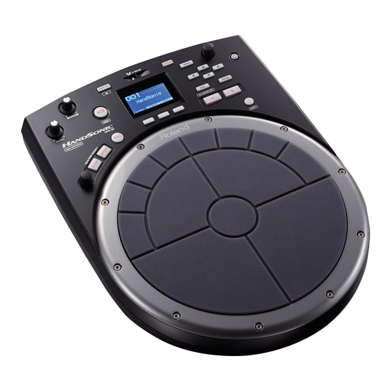
Page 4: Location Of Controls
Sep. 2013 HPD-20 Location of Controls fig.panel.eps... -
Page 5: Location Of Controls Parts List
Sep. 2013 HPD-20 Location of Controls Parts List Top Panel Part Code Part Name Description Q’ty 5100034514 TOP CASE 04897934 J R-KNOB SF-ELA BLK/SLV HS 02891812 12M/M ROTARY POTENTIOMETER RK12L12C0C08 03565789 M R-KNOB LF-ELA BLK 5100036689 ENCODER EC09E1520406 5100029775 LED(INFRARED) L-7113F3C(F) 5100030358 DIODE... -
Page 6: Exploded View
Sep. 2013 HPD-20 Exploded View fig.bunkai-all.eps... -
Page 7: Exploded View Parts List
Sep. 2013 HPD-20 Exploded View Parts List Part Code Part Name Description Q’ty 5100034516 PAD HOOP 5100034517 PLAYING PLATE 5100036155 UPPER CUSHION 5100036156 LOWER CUSHION 5100034513 PRESSURE SHEET SENSOR 5100034508 SENSOR BOARD ASSY 04897934 J R-KNOB SF-ELA BLK/SLV HS 03565789 M R-KNOB LF-ELA BLK 5100000903... -
Page 8: Plane View (View 1, 2)
Sep. 2013 HPD-20 Plane View (View 1, 2) fig.heimen1.eps View 1 View 2 View 1 Part Code Part Name Description Q’ty 5100028090 SCREW 3X10 HEX SOCKET HEAD TAPTITE P NI View 2 Part Code Part Name Description Q’ty 40011312 SCREW 3X8 BINDING TAPTITE P FE BZC... -
Page 9: Plane View (View 3, 4, 5, 6)
Sep. 2013 HPD-20 Plane View (View 3, 4, 5, 6) fig.heimen2.eps View 3 View 4 View 5 View 6 View 3 Part Code Part Name Description Q’ty 40011067 SCREW 3X8 BINDING TAPTITE B FE ZC View 4 Part Code Part Name Description Q’ty 40011323... -
Page 10: Plane View (View 7, 8, 9)
Sep. 2013 HPD-20 Plane View (View 7, 8, 9) fig.heimen3.eps View 7 View 9 View 8 View 7 Part Code Part Name Description Q’ty 40011312 SCREW 3X8 BINDING TAPTITE P FE BZC View 8 Part Code Part Name Description Q’ty 40013056 SCREW M3X6 PAN MACHINE W/SW+PW(S) ZC... -
Page 11: Important Notes On Assembly
Sep. 2013 HPD-20 Important Notes on Assembly PLAYING PLATE Attach the playing plate (with cushion). fig.kumitate4-e.eps When attaching the playing plate (#5100034517) to the upper cushion (#5100036155) and the lower cushion (#5100036156), give attention to the following points. Attach the playing plate to the upper cushion. fig.kumitate1-e.eps Note: For positioning pin... - Page 12 Sep. 2013 HPD-20 Flat Cable (CN900) When disconnecting the flat cable (#5100035570) connected to the Sensor Board Assy (#5100034508), follow the procedure described below to assembly. Secure the Sensor Board Assy to the top case using screws. Insert the flat cable (CN900). Secure the Bottom Case.
-
Page 13: Parts List
• Reissuance is restricted. only listed parts for replacement. • It is carried in electronic data on the Roland web site. • It is supplied as an assembled part • The part is made to order (at current market price). - Page 14 Sep. 2013 HPD-20 PICK UP, SENSOR 5100034513 PRESSURE SHEET SENSOR 5100034556 SENSOR ASSY SCREWS 40013056 SCREW M3X6 PAN MACHINE W/SW+PW(S) ZC 40230745 SCREW M5X25 TRUSS MACHINE BZC 40011067 SCREW 3X8 BINDING TAPTITE B FE ZC 40011312 SCREW 3X8 BINDING TAPTITE P FE BZC 40011323 SCREW 3X10 BINDING TAPTITE P BZC...
-
Page 15: Wiring Diagram
Sep. 2013 HPD-20 Wiring Diagram fig.wiring.eps CN700 CN701 Part Code Part Name Description Q’ty 5100035569 FLAT CABLE FFC A-1.0-34X120-4/8-0.7X0.05 5100035563 FLAT CABLE FFC A-1.0-32X80-4/8-0.7X0.05 5100035570 FLAT CABLE FFC A-1.0-16X100-4/8-0.7X0.05 5100035564 FLAT CABLE FFC A-1.0-28X140-4/8-0.7X0.05 5100035571 WIRING 1061#28 8X70-PHR-PHR-F ********** included in LCD CMF2P0791-E (C3700007R0) (#5100020820) ********** included in LCD CMF2P0791-E (C3700007R0) (#5100020820) **********... -
Page 16: Block Diagram
Sep. 2013 HPD-20 Block Diagram fig.block.eps@L... - Page 17 Sep. 2013 HPD-20 fig.block.eps@R...
-
Page 18: Verifying The Version
F1, F2, and F3. * Do not strike the HandSonic’s pads while data is being saved. The vibration may cause unexpected errors. * Backup files are saved in the Roland/HPD-20/Backup folder of the USB Verifying the Version memory device. -
Page 19: Performing A Factory Reset
Make a backup beforehand. (Refer to Data Backup and Restore Operations (p. 18).) (BKUP-001.HS0) to the Roland/HPD-20/Backup folder on the USB memory device and restore it. (Refer to Data Backup and Restore Operations (p. 18).) Items Required •... - Page 20 Sep. 2013 HPD-20 Test Items 3. FOOT SW 1. VERSION (p. 20) fig.test-5.eps 2. MIDI (p. 20) 3. FOOT SW (p. 20) 4. SW/LED (p. 20) 5. CONTRAST/ENC (p. 21) 6. BACKLIGHT/ENC (p. 21) 7. D-BEAM (p. 21) * Before entering this test item, connect the FS-5 (2) to the FOOT SW jack. 8.
- Page 21 Sep. 2013 HPD-20 5. CONTRAST/ENC 7. D-BEAM fig.test-7.eps fig.test-9.eps This tests the operation of the encoder at the lower left of the panel and * The relation between the on-screen values and the height varies according to the changes in the contrast of the LCD screen. surrounding environment (brightness and color of illumination).
- Page 22 Sep. 2013 HPD-20 8. PAD PRESS 9. PAD VELOCITY fig.test-12.eps fig.test-15.eps * Look out for the big sound. * Look out for the big sound. The test program automatically checks whether or not the pressure value Strike the two large pads built-in piezo sensors (M1, M2) with weak, changes.
- Page 23 Sep. 2013 HPD-20 11. HH CTRL 14. DEVICE fig.test-19.eps fig.test-22.eps The operation of each device is tested automatically. * Before entering this test item, connect the foot pedal (FD-8, etc.) to the HH CTRL jack. Test Items Slowly and gradually depress the foot pedal, and verify that the on- •...
- Page 24 Sep. 2013 HPD-20 15. MIX IN 17. PHONES fig.test-23.eps fig.test-25.eps * Look out for the big sound. * Look out for the big sound. * If possible, use an oscilloscope to verify that the waveform shows no distortion or * If possible, use an oscilloscope to verify that the waveform shows no distortion or abnormal oscillation.
- Page 25 Sep. 2013 HPD-20...
-
Page 26: Circuit Board (Main Board)
Sep. 2013 HPD-20 Circuit Board (Main Board) fig.b-main1.eps... - Page 27 Sep. 2013 HPD-20 fig.b-main2.eps...
-
Page 28: Circuit Diagram (Main Board: 1/4)
Sep. 2013 HPD-20 Circuit Diagram (Main Board: 1/4) fig.d-main1.eps@L D+3.3V MAIN, Memory RA35 RA36 EXB28V472JX EXB28V472JX D+3.3V 24FLT-SM2-TB (LF)(SN) 0.1uF R271 UnPop 4.7k 4.7k UnPop DGND EXB28V330JX AUDCK AUDATA0 AUDATA1 AUDATA2 AUDATA3 AUDSYNC XTRST XASEMD D+3.3V <2B1;2D1> R111 XCCS3 XRESET-RST XCCS0 <E2>... - Page 29 Sep. 2013 HPD-20 fig.d-main1.eps@R CA(22:1) <2A1> CA(22) RA44 CA(21) FSW1 DMPXIN1 <D3> EXB28V680JX CA(20) <4D5> ENC1B DMPXIN0 <D3> CA(19) <4C1> ENC0B CA(18) <4C1> RIMSW CA(17) <4D5> FSW0 CA(16) <4D5> ENC1A CA(15) <4C1> D+3.3V ENC0A CA(14) <4C1> HEADSW CA(13) <4D5> AA25 CA(12) EXB28V680JX RA40...
-
Page 30: Circuit Diagram (Main Board: 2/4)
Sep. 2013 HPD-20 Circuit Diagram (Main Board: 2/4) fig.d-main2.eps@L ADP+9V D+3.3V SSC(Local bus), R108 Power 1608 10uF EXCML16A270U 2125 DGND 10uF CD(31:0) <1B5> 2125 100pF CA(22:1) CD(31) DQ15 0.1uF <1A5> CD(30) DQ14 CD(29) <C1> MEMS0 EXB28V101JX DQ13 CD(28) CA(13) RA51 DGND DGND 47uH... - Page 31 Sep. 2013 HPD-20 fig.d-main2.eps@R D+5V R109 QS8J4TR EXCML16A270U 2SA1832-GR(TE85L.F) PWR+5V 1608 1608 100pF 100k 220uF 1000pF DGND CDRH3D18NP-150NC-R D+3.3V 15uH 5.6B DGND 10uF 10uF PGND1 2012 2012 UnPop ITH1 PGND1 DGND DGND D+1.2V CDRH3D18NP-150NC-R 15uH C228 C221 10uF 10uF PGND2 2012 2012 UnPop...
-
Page 32: Circuit Diagram (Main Board: 3/4)
Sep. 2013 HPD-20 Circuit Diagram (Main Board: 3/4) fig.d-main3.eps@L MAIN BOARD (DSP/Memory, D/A,Interface) D+3.3V IC21 C383 TC7WU04FU(TE12L.F) 0.1uF <4B1> SCAN4 R368 (Wave FLASH) XWCS0 R317 <B6> IC21 R168 <4B1> SCAN3 DGND TC7WU04FU(TE12L.F) R169 <4A1> SCAN2 R122 SCAN1 <4A1> R119 <4A1> SCAN0 R118 <4D1>... - Page 33 Sep. 2013 HPD-20 fig.d-main3.eps@R WD(15:0) WA(27:1) D+3.3V D+3.3V R134 XWCS1 <D5> for 1Gbit WA(27) R124 A-MUTE <4D5> R279 C387 C389 C438 R142 0.1uF USBON <1C6> 0.1uF 10uF 2012 WA(26) WA(24) WA(23) WA(22) DGND DGND DGND C282 WA(21) 22pF WA(20) WA(19) RA47 WD(15) DQ15/A-1...
-
Page 34: Circuit Diagram (Main Board: 4/4)
Sep. 2013 HPD-20 Circuit Diagram (Main Board: 4/4) fig.d-main4.eps@L D+3.3V D+5V C129 C125 2012 2012 10uF 10uF C132 C131 28FMN-BMTTN-A-TFT (LF)(SN) IC17 R129 0.1uF 0.1uF TC74VHC14FT(EL.K) TP104 DGND DGND PSW-DET D+3.3V TP103 <3D5> TP115 TP105 TP102 UDZS TE-17 5.6B TP106 TP116 TP117 TP93... - Page 35 Sep. 2013 HPD-20 fig.d-main4.eps@R A+9V 0.1uF C257 AGND 0.1uF NJM4565M-D(TE2) C267 AGND A-9V A+5V 3.4Vpp 3.4Vpp/2=1.7Vpeak 1.202Vrms 20log(1.202/0.775)=3.81dBu R140 R162 1608 3.4Vpp 12Vpp 1608 C230 20log(3.6)=11.12dB 10uF R146 R151 390pF 2012 3.3k 2.7k 1608 C137 1608 1608 C253 C237 C161 0.1uF 3300pF 10uF...
-
Page 36: Circuit Board (Panel, Jack, Jksub Board)
Sep. 2013 HPD-20 Circuit Board (Panel, Jack, Jksub Board) fig.b-JKPNL1.eps... - Page 37 Sep. 2013 HPD-20 fig.b-JKPNL2.eps...
-
Page 38: Circuit Diagram (Panel Board: 1/4)
Sep. 2013 HPD-20 Circuit Diagram (Panel Board: 1/4) fig.d-panel1.eps@L D+3.3V_P D+5V_P C546 C547 100uF 100uF C553 C551 0.1uF 0.1uF DGND_P DGND_P TP605 TP606 TP607 TP608 TP609 TP612 TP610 TP614 TP611 TP613 TP617 SCAN0 <3A1> TP615 SCAN1 <3B1> TP619 SCAN2 <3B1> TP616 SCAN3 <3C1>... - Page 39 Sep. 2013 HPD-20 fig.d-panel1.eps@R LCD CONNECTION D+5V_P D+3.3V_P C571 10uF 2012 C500 0.1uF DGND_P R514 TO_LCD-CS LCD-CS <D3> TP669 R512 TO_LCD-RST LCD-XRST <D3> TP666 R510 LCD-RS TP668 <D3> TO_LCD-CLK R509 TP670 C570 10uF R511 TO_LCD-DATA LCD-SCK <D3> TP671 CN500 2012 TP672 S2B-PH-K-S (LF)(SN) R513...
-
Page 40: Circuit Diagram (Panel Board: 2/4)
Sep. 2013 HPD-20 Circuit Diagram (Panel Board: 2/4) fig.d-panel2.eps@L 28FMN-BTK-A (LF)(SN AGND_POST P CN504 HHC P <4C3> TP557 TP558 EXTTRG-HP <4D3> TP559 EXTTRG-R P <4C3> TP560 TP561 TP562 PHOR-RTNP-SI G TP563 TP564 PHOL-RTNP-SI G TP565 TP566 TP567 MASL-SNDP-SI G TP570 TP578 TP571 MASR-SNDP-SI G... - Page 41 Sep. 2013 HPD-20 fig.d-panel2.eps@R UnPop R545 IC50 2 1608 C576 NJM4565M-D(TE2 ) 22pF C587 10uF C589 10uF VR500 VR500 R534 RK12L12C0C0 8 RK12L12C0C0 8 10kA 10kA 1608 100k 100k R539 R544 AGND_POST P AGND_POST P AGND_POST P AGND_POST P UnPop R546 A+9V_P C575...
-
Page 42: Circuit Diagram (Panel Board: 3/4)
Sep. 2013 HPD-20 Circuit Diagram (Panel Board: 3/4) fig.d-panel3.eps@L D+3.3V_P R551 R550 R549 1608 1/2W 1/2W C604 5025 5025 PITCH ROLL UnPop EFFECT UnPop D504 D509 100uF UnPop 1SS361FV(TPL3.Z) 1SS361FV(TPL3.Z) DGND_P SW501 SW500 SW502 SW503 CARBON_SW PC043-14 CARBON_SW PC043-15 CARBON_SW PC043-07 CARBON_SW PC043-06 Q511 <1A3>... - Page 43 Sep. 2013 HPD-20 fig.d-panel3.eps@R LED510 SML-212U2TT86A EFFECT LED505 SML-212U2TT86A EN501 EC09E1520406 LED502 EN501 SML-212U2TT86A EC09E1520406 D-BEAM ENC0B <1D3> DGND_P ENC0A <1C3> LED501 EN500 SML-212U2TT86A EC09E1520406 EN500 EC09E1520406 ENC1B <1D3> DGND_P ENC1A LED504 <1D3> SML-212U2TT86A ENTER R555 1608 Q507 2SC4738-GR(TE85L.F) LEDO1 R548 R552 1608...
-
Page 44: Circuit Diagram (Panel Board: 4/4)
Sep. 2013 HPD-20 Circuit Diagram (Panel Board: 4/4) fig.d-panel4.eps@L TP532 TP523 TP524 R603 R567 1SS362FV(TPL3) DGND_P D517 R610 TP516 R592 TP531 D519 TP517 TP520 TP522 TP530 M1 Piezo C628 22pF C624 22pF TP535 R599 1608 D515 R578 1608 B2B-PH-K-S (LF)(SN) CN700 D518 B2B-PH-K-S (LF)(SN) - Page 45 Sep. 2013 HPD-20 fig.d-panel4.eps@R TP546 TP545 M1-PIEZO <C3> R562 C623 M2-PIEZO <C3> 1608 TP543 TP539 R596 DGND_P R568 R556 1SS362FV(TPL3) C622 DGND_P R609 1608 R593 D516 TP541 C625 22pF C626 22pF DGND_P R597 D514 R602 A+9V_P IC508 IC508 BA2902FV-E2 DGND_P TP540 BA2902FV-E2 TP538...
-
Page 46: Circuit Diagram (Jack Board: 1/3)
Sep. 2013 HPD-20 Circuit Diagram (Jack Board: 1/3) fig.d-jack1.eps@L JACK BOARD (sheet1: Connector, MIXIN, Power) RB051L-40 TE25(PB FREE) QS8J4TR ERBRG1R50V DC-IN 3216 open 0.1uF 100k 0.1uF HEC0470-01-630 1608 1608 1608 220k PLA10AN5521R0R2B 1608 1608 2.2k AGND_POST 1608 NC-X SYMBOL UDZS TE-17 11B 2SC4081 T106 QRS (PB FREE) 100k SW-PW... - Page 47 Sep. 2013 HPD-20 fig.d-jack1.eps@R D+3.3V D+5V 10uF 10uF 2012 2012 0.1uF 0.1uF DGND DGND ADP+9V DGND QS8J4TR 100k 220uF 1608 1608 HEADSW <2A6> RIMSW <2B6> AGND_POST FSW0 <2C6> FSW1 <2D6> MIDI-IN <2F4> 2SA1037AKT146(PB FREE ) MIDI-OUT <2E3> SW-PW <B3> POWERON <C3>...
-
Page 48: Circuit Diagram (Jack Board: 2/3)
Sep. 2013 HPD-20 Circuit Diagram (Jack Board: 2/3) fig.d-jack2.eps@L D+3.3V D+3.3V JACK BOARD 1SS362FV(TPL3) 100k (sheet2: TRIG, MIDI) 1608 DGND 1608 TC74VHC14FT(EL.K) 0.01uF R107 DGND 1SS362FV(TPL3) DGND R104 1608 DGND 22pF 22pF R106 1608 DGND R101 100k 0.22uF 1608 IC5 BA2902FV-E2 IC5 BA2902FV-E2 R100 DGND... - Page 49 Sep. 2013 HPD-20 fig.d-jack2.eps@R HEADSW <1A7> A+9V EXTTRG-H <3A2> EXTTRG-R C141 <3B2> 0.1uF BA2902FV-E2 DGND C140 1SS362FV(TPL3) 0.1uF 1608 A-9V 22pF DGND IC5 BA2902FV-E2 A+9V C149 0.1uF IC10 UnPop BA2902FV-E2 UnPop DGND DGND C148 IC10 BA2902FV-E2 0.1uF UnPop UnPop RIMSW <1A7>...
-
Page 50: Circuit Diagram (Jack Board: 3/3)
Sep. 2013 HPD-20 Circuit Diagram (Jack Board: 3/3) fig.d-jack3.eps@L JACK BOARD (sheet3: Connector, AUDIO OUT) To PANEL BAORD 28FMN-STK-A (LF)(SN) DGND <2D6> <2A6> EXTTRG-H <2A6> EXTTRG-R AGND_POST PHOL-RTN-SIG AGND_PRE PHOR-RTN-SIG MASL-RTN-SIG 1608 C230 22pF R255 <1C5> MIXIN-L 1608 R288 1608 IC20 NJM4565M-D(TE2) R259... - Page 51 Sep. 2013 HPD-20 fig.d-jack3.eps@R A+9V C199 100uF C166 0.1uF AGND_POST IC19 A+9V A-9V NJM4556AD C195 0.1uF C196 100uF C220 C224 1608 C198 C197 OpAmp Gain = 6.74 C172 100pF 10uF 10uF 0.1uF 0.1uF Phones Amp Gain = 6.14 = +15.76dB A-9V AGND_POST R233...
-
Page 52: Circuit Diagram (Jksub Board)
Sep. 2013 HPD-20 Circuit Diagram (Jksub Board) fig.d-jksub.eps Tip : FOOT SW 0 Ring: FOOT SW 1 R1005 1608 R1008 1608 R1004 1608 JK1000 LGR4609-7100F C1002 C1000 100pF 100pF 1608 1608 DGND_JS DGND_JS DGND_JS FS1002 NC-X SYMBOL TRIG IN R1006 1608 R1003 CN1000... -
Page 53: Circuit Board (Sensor Board)
Sep. 2013 HPD-20 Circuit Board (Sensor Board) fig.b-sensor.eps Circuit Diagram (Sensor Board) fig.d-sensor.eps CN900 16FMN-BTK-A (LF)(SN) SW903 SW900 SUBPAD1 SW910 SUBPAD5 SW906 SUBPAD2 SW908 SUBPAD6 SW905 SUBPAD3 SW907 SUBPAD7 SW904 SUBPAD4 SW901 SUBPAD8 SW902 MAINPAD3 SW911 MAINPAD4 SW909 MAINPAD5 SW912 MAINPAD2 MAINPAD1 DGND_S...
Need help?
Do you have a question about the HandSonic HPD-20 and is the answer not in the manual?
Questions and answers