Advertisement
Quick Links
LX7720 Daughter Board User Guide
Description
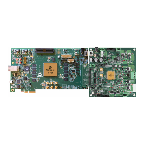
The LX7720 daughter board contains a soldered in place LX7720-ES and peripherals to allow
quickly evaluated. Demonstration firmware is available for
The LX7720 daughter board uses a high pin count (HPC) FMC connector for plug-in connection to an
KIT
(Figure 1 on page 1), an
SmartFusion2
SoC FPGA M2S150-ADV-DEV-KIT. A 40-way header provides the same signals for connection to other
FPGA boards such as a
RT ProASIC3
to route signals from the 40-way header to a
TFBGA-EK
evaluation kit (Figure 3 on page 2) or a
Kit Contents
•
LX7720 evaluation board SOL-12-000003-11 with soldered-in-place LX7720-ES engineering sample
•
Engineering sample (-ES marking suffix) explanation sheet
•
24V 1.5A universal input AC adapter with 2.1mm x 5.5mm DC output connector, centre positive
•
20x 0.1" pitch shorting jumpers
•
2x 2-position 5mm pitch terminal block sockets type A, Adam Tech EB9A-02-C or equivalent to mate J30, and J31
•
2x 2-position 5mm pitch terminal block sockets type B, Molex 0395237002 or equivalent to mate J12 and J18
•
4-position 5mm pitch terminal block socket type B, Molex 0395237004 or equivalent, to mate J9
•
3-position 2.54mm pitch wire crimp housing Molex 50-57-9403 (latching) or 50-57-9003 (non-latching) to mate J13
•
6-position 2.54mm pitch wire crimp housing Molex 50-57-9406 (latching) or 50-57-9006 (non-latching) to mate J14
•
8-position 2.54mm pitch wire crimp housing Molex 50-57-9408 (latching) or 50-57-9008 (non-latching) to mate J15
•
20x Molex 16-02-0096 crimp sockets to suit 24 - 30AWG wire, for J13, J14, and J15 housings
•
Linker board to connect to a
•
Linker board to connect to a
•
Linker board to connect to a
•
4x 6mm, 4x 7mm, 4x 8mm, 5x 20mm, 1x 38mm nylon standoffs and 13x nuts for linker board height matching
•
USB stick with documentation (see section 3 on page 3)
Ordering Information
Product
LX7720 Daughter Board
Figure 1. LX7720 Daughter Board Connected to
© 2023 Microchip Technology Inc.
RT PolarFire
FPGA RTPF-DEV-KIT, a
FPGA
ProASIC3 Starter
SAMRH71F20
SAMRH707F18
SAMRH71F20-EK
evaluation kit, plus a board with control switches and LEDs
SAMRH71-TFBGA-EK
SAMRH707F18-EK
evaluation kit, with LC filters for optional ∆Σ stream processing
Order Number
LX7720-DB
RTG4 DEV-KIT
RTG4
FPGAs and
SAM
PolarFire
FPGA MPF300-EVAL-KIT, or a
Kit, that lack FMC connectivity. Linker boards are included
MCU
Evaluation Kit
(Figure 2 on page 2) and
MCU
Evaluation Kit
evaluation kit (which can also use the switch/LED board)
using the HPC FMC Connector
LX7720 Daughter Board User Guide rev 3.1 - page 1
LX7720
functionality to be
rad hard MCUs.
RTG4
SAMRH71-
(Figure 4 on page 2).
FPGA
DEV-
Advertisement

Related Manuals for Microchip Technology LX7720


Summary of Contents for Microchip Technology LX7720
- Page 1 Demonstration firmware is available for RTG4 FPGAs and rad hard MCUs. The LX7720 daughter board uses a high pin count (HPC) FMC connector for plug-in connection to an RTG4 FPGA DEV- (Figure 1 on page 1), an...
- Page 2 Figure 3. LX7720 Daughter Board Connected to SAMRH71-TFBGA-EK Evaluation Kit Using Included Linker Board Figure 4. LX7720 Daughter Board Connected to SAMRH707F18-EK Evaluation Kit Using Included Linker Board © 2023 Microchip Technology Inc. LX7720 Daughter Board User Guide rev 3.1 - page 2...
- Page 3 FMC Connection to FPGA Evaluation Boards The LX7720-DB uses an HPC-FMC, J10, for signals to and from an external FPGA board, discussed in detail in Section 7 on page 17. Pinouts and FPGA resource allocations are provided for the following FPGA boards' HPC1-FMC connector: •...
- Page 4 Board Sockets and Link Configuration Figure 5 below identifies major circuit blocks, LEDs, and connectors. Figure 6 on page 5 identifies link headers that configure signal and power supply options on the board, and set LX7720 pin configurations. Table 1 on page 5 summarizes the functions of all connectors and link headers, and provides clickable links to the appropriate parts of section 5 starting on page 8, which provides more detail and schematic around each one.
- Page 5 Select shorter DMOD_OUT_N pin 44 and DMOD_OUT_P pin 46 driver page 15 propagation Pin 1 to VDD propagation delay by setting LX7720 DMOD_BW pin 114 = high. Nearby VDD delay points include J38 pin 1 and J40 pin 1 © 2023 Microchip Technology Inc.
- Page 6 Couple the filtered resolver/LVDT driver outputs LX7720 DMOD_OUT_N pin 44 Resolver/LVDT 5.14, Link 1 to 2 and DMOD_OUT_P pin 46 to LX7720 ADC3_N pin 36 and ADC3_P pin 37 for driver page 15 measurement of the drive amplitude and fault detection...
- Page 7 Managed by 5.11, page 13 Link 2 to 3 pin G16 or 40 pin header J20 pin 31. A pull-down resistor ensures that LX7720 controller on remains out of reset condition if the external signal is open J10 or J20...
- Page 8 The header J32 selects either the on-board 15V regulator, or an external 10V to 18V power supply connected to J31 (Table 2, Figure 10). If LX7720's internal VEE charge pump is used (section 5.4 on page 10), VGS = 12V not 10V.
- Page 9 VCC_R 12V/15V_VIN_U10 0/0805 37.4k/1%/0805 HDR_3_100MIL 1uF/25V/0805 0.1uF/25V/0805 0.1uF/25V/0805 4.7uF/25V/0805 REG103GA-A 13k/1%/0805 HDR_2_100MIL C116 C117 0.1uF/25V/0805 4.7uF/25V/0805 LTST-C190GKT OSTOQ02715 GREEN,10mA 300R/0805 Figure 11. 5V Regulator Schematic © 2023 Microchip Technology Inc. LX7720 Daughter Board User Guide rev 3.1 - page 9...
- Page 10 J18 (Table 5, Figure 13). While the LX7720 allows a logic supply range of 2.1V to 5.5V, the LX7720 daughter board's allowed range is 2.7V to 3.6V. This limitation is due to the supply range of the 27MHz oscillator module Y2, and the SN74LVTH16245A bus transceivers that interface both the 2x20 pin controller interface header J20 and the RTG4 interface FMC connector J10.
- Page 11 Figure 13. VDD Logic Supply (3.3V) Regulator Schematic Reference Voltage Selection The 3-pin header J1 selects either the LX7720's internal 2.5V ±0.8% reference or an external reference U2, adjustable by potentiometer R3 (Table 6, Figure 14). The adjustment range is 2.3V to 2.7V.
- Page 12 Charge Pump CP_CLK Selection There are 4 possible sources for the 100kHz to 300kHz charge pump clock, CP_CLK_D at LX7720 pin 13. The 2x20 pin controller interface header J20 and RTG4 Interface FMC connector J10 are wired in parallel to deliver an external clock CP_CLK_C, which is buffered by a gate in U12 (SN74LVTH16245A) to become CP_CLK.
- Page 13 Link 2 to 1 Reset clears latched OC_FAULT, PR_FAULT, and/or over-temperature shutdown faults LX7720 RESET pin 18 is controlled by an external signal on FMC connector J10 pin G16 (RTG4 board) or 40 pin header J20 pin 31 (other controller).
- Page 14 Bi-Level Comparator Inputs BL1 to BL6 The LX7720's 6 bi-level comparator inputs BLI1 to BLI6 are routed to connector J15 pins 3 to 8 respectively. The common comparator threshold LX7720 BLI_TH pin 119 is set to VCC/2 by R4 & R5.
- Page 15 Links J5 to J8 configure the resolver/LVDT driver outputs with or without LC filtering for primary drive wave shaping. Link J5 is left open by default to set LX7720 DMOD_BW pin 114 = low, selecting the longer DMOD_OUT_N pin 44 and DMOD_OUT_P pin 46 driver propagation delay.
- Page 16 ±2.14A as the effective current sense resistance drops from 0.25Ω to 0.117Ω. Control and Acquisition Signals Header J20 J20 is a 2x20 pin 0.1" pitch pin header which provides access to LX7720 signals (Table 14 on page 16) to an external control system without FMC support.
- Page 17 Height Matching the LX7720MLF-EVB and Target FPGA Boards The LX7720-DB needs to be 10mm higher in height than the target FPGA board for the heights to match with the FMC connectors mated (presuming a standard 1.6mm FPGA board PCB thickness). The LX7720-DB is fitted as standard with four 25mm standoffs for feet.
- Page 18 LX7720 Daughter Board User's Manual FMC-HPC Connector J10 Table 16. LX7720 Control and Acquisition Signals HPC-FMC Connector J10 Pinout (F to K) Signal Signal Signal Signal Signal UD_IN_C_C CLK_OUT_C LD_IN_B_C MOD_CLK_C ADC3_C ADC2_C LD_IN_A_C SNS_OUT_A_C SNS_OUT_D_C SNS_OUT_B_C SNS_OUT_C_C RESET SM_EN...
- Page 19 LX7720 Daughter Board User's Manual FMC-HPC Connector J10 Table 17. Mapping of HPC1-FMC pins, LX7720 pins, and RTG4 and PolarFire FPGA pins LX7720 Signal RTG4 Pin RTG4 Pin PolarFire PolarFire Pin LX7720 Signal Type and Function Name Number Name Pin Number...
- Page 20 LX7720 Daughter Board User's Manual FMC-HPC Connector J10 Table 18. Mapping of HPC1-FMC Pins, LX7720 Functionality, and RT-Polarfire FPGA Pins LX7720 Signal RT-Polarfire FMC RT-Polarfire RT-Polarfire LX7720 Signal Type and Function Name Net Name Pin Number Pin Name ADC2 bit stream output...
- Page 21 LX7720 Daughter Board User's Manual FMC-HPC Connector J10 Table 19. Mapping of HPC1-FMC pins, LX7720 pins, and SmartFusion2 SoC FPGA pins LX7720 Signal SmartFusion2 SmartFusion2 SmartFusion2 LX7720 Signal Type and Function Name FMC Net Name Pin Number Pin Name ADC1_C...
- Page 22 If the LX7720-DB is using 25mm standoffs, fit the included 20mm standoffs to the SAMRH71F20-TFBGA-EK • If the LX7720-DB is using 8mm standoffs, join the included 6mm and 7mm standoffs to make 13mm standoffs and fit these to the SAMRH71F20-TFBGA-EK...
- Page 23 LX7720 Daughter Board User's Manual SAMRH71F20(-TFBGA)-EK to LX7720-DB Linker Boards Table 21. Linker Board Mapping of SAMRH71F20 and LX7720 Functionality LX7720 Signal LX7720 Function SAMRH71 Function Timer Motor Phase Waveform Generation LD_IN_A Motor phase A lower FET PWM PWMC0_PWML0 UD_IN_A...
- Page 24 PCB foil patterns for the two linkers are shown in Figure 34 and Figure 35 on page 35. Figure 23. SAMRH71F20-TFBGA-EK Linker Schematic © 2023 Microchip Technology Inc. LX7720 Daughter Board User Guide rev 3.1 - page 24...
- Page 25 LX7720 Daughter Board User's Manual SAMRH71F20(-TFBGA)-EK to LX7720-DB Linker Boards Figure 24. SAMRH71F20-EK Linker and Switch Board Schematic © 2023 Microchip Technology Inc. LX7720 Daughter Board User Guide rev 3.1 - page 25...
- Page 26 LX7720 Daughter Board User's Manual SAMRH71F20(-TFBGA)-EK to LX7720-DB Linker Boards Figure 25. SAMRH71F20-EK to LX7720-DB Linker Board PCB Layout Figure 26. SAMRH71F20-TFBGA-EK to LX7720-DB Linker Board PCB Layout © 2023 Microchip Technology Inc. LX7720 Daughter Board User Guide rev 3.1 - page 26...
- Page 27 ∆ on the IDC connector will be pointing to J25/J9 pins 1 and 2 (NC and GND. The ribbon cable direction will be away from the top of the boards. Figure 27. SAMRH71F20-EK to LX7720-DB Linker Board Ribbon Cable Construction © 2023 Microchip Technology Inc.
- Page 28 All four LX7720 half-bridges are routed by default to MCU PWM outputs, for BLDC and stepper compatibility. The fitted 0Ω resistors R1 and R2 connect the 4th pair of MCU PWM outputs to the 4th LX7720 half-bridge. This default configuration suits operation of either a 3-phase BLDC without resolver/LVDT, or a bipolar stepper motor •...
- Page 29 LX7720 Daughter Board User's Manual LX7720-DB to SAMRH707F18-EK v1 Linker Board the ADC's reference. Selecting the LX7720's 3.3V logic supply allows the filters to be powered and evaluated for debug purposes without connecting a SAMRH707F18-EK. The LX7720's ∆Σ serial streams for the four current sensing channels SNS_OUT_A to SNS_OUT_D are high for full scale positive current (350mV across the current sense resistor), low for full scale negative current (-350mV across the current sense resistor), and average 50% high, 50% low for zero current.
- Page 30 LX7720 Daughter Board User's Manual LX7720-DB to SAMRH707F18-EK v1 Linker Board Table 24. Linker Board Mapping of SAMRH707F18-EK and LX7720 Functionality LX7720 Signal LX7720 Function SAMRH707 Function Motor Phase Waveform Generation UD_IN_A Motor phase A upper FET PWM PWMC0_PWMH0 (and green LED0 on the -EK)
- Page 31 The SAMRH707F18-EK linker's schematic is shown in Figure 32 below. The PCB foil pattern is shown in Figure 33 on page 32. Figure 32. SAMRH707F18-EK to LX7720-DB Linker Board Schematic © 2023 Microchip Technology Inc. LX7720 Daughter Board User Guide rev 3.1 - page 31...
- Page 32 LX7720 Daughter Board User's Manual SAMRH707F18-EK Linker Board Schematic and PCB Layout Figure 33. SAMRH707F18-EK to LX7720-DB Linker Board PCB Layout Top and Bottom Views © 2023 Microchip Technology Inc. LX7720 Daughter Board User Guide rev 3.1 - page 32...
- Page 33 SAMRH707F18-EK Linker Board Schematic and PCB Layout 10.1 SAMRH707F18-EK to LX7720-DB Linker Board Parts List The parts list for the SAMRH707F18-EK to LX7720-DB linker board is shown below in Table 25 below. Table 25. SAMRH707F18-EK to LX7720-DB Linker Board Bill of Materials Designator...
- Page 34 LX7720 Daughter Board User's Manual LX7720-DB Complete Schematics LX7720-DB Complete Schematics Figure 34. LX7720-DB Power Connection © 2023 Microchip Technology Inc. LX7720 Daughter Board User Guide rev 3.1 - page 34...
- Page 35 LX7720 Daughter Board User's Manual LX7720-DB Complete Schematics Figure 35. LX7720-DB FPGA and Sensor Connection © 2023 Microchip Technology Inc. LX7720 Daughter Board User Guide rev 3.1 - page 35...
- Page 36 LX7720 Daughter Board User's Manual LX7720-DB Complete Schematics Figure 36. LX7720-DB Motor/Driver Connection © 2023 Microchip Technology Inc. LX7720 Daughter Board User Guide rev 3.1 - page 36...
- Page 37 LX7720 Daughter Board User's Manual LX7720-DB Complete Schematics Figure 37. LX7720-DB Line Drivers and Dual Row Header, Power Section © 2023 Microchip Technology Inc. LX7720 Daughter Board User Guide rev 3.1 - page 37...
- Page 38 LX7720 Daughter Board User's Manual LX7720-DB Complete Schematics Figure 38. LX7720-DB FMC Connector to FPGA Board © 2023 Microchip Technology Inc. LX7720 Daughter Board User Guide rev 3.1 - page 38...
- Page 39 LX7720 Daughter Board User's Manual LX7720-DB Complete Schematics Figure 39. LX7720-DB 50V Input to 15V, 12V to 15V Input to 5V, and 12V to 15V Input to 3.3V Regulators © 2023 Microchip Technology Inc. LX7720 Daughter Board User Guide rev 3.1 - page 39...
- Page 40 LX7720 Daughter Board User's Manual LX7720-DB PCB Layout LX7720-DB PCB Layout Figure 40. LX7720-DB PCB Top Copper Layer 1 and Component IDs (Rev. E) © 2023 Microchip Technology Inc. LX7720 Daughter Board User Guide rev 3.1 - page 40...
- Page 41 LX7720 Daughter Board User's Manual LX7720-DB PCB Layout Figure 41. LX7720-DB PCB Bottom Copper Layer and Component IDs Bottom View (Rev. E) © 2023 Microchip Technology Inc. LX7720 Daughter Board User Guide rev 3.1 - page 41...
- Page 42 This parts list covers the D and E revisions. Differences are identified for affected part numbers in the parts list below. Figure 42 below shows how to identify board version in the bottom right corner. Figure 42. Identifying LX7720-DB Rev D boards (left) and Rev E boards (right) Table 26. LX7720-DB Bill of Materials...
- Page 43 150R/0805 RNCP0805FTD150R Stackpole RES 150Ω 1% 1/4W 0805 R106, R107, R112, R113, R120, R121, 10K/1%/0805 RC0805FR-0710KL Yageo RES SMD 10KΩ 1% 1/8W 0805 R125, R126 © 2023 Microchip Technology Inc. LX7720 Daughter Board User Guide rev 3.1 - page 43...
- Page 44 Added FMC connector IDs on RTG4 Development Kit and PolarFire MPF300-EVAL-KIT in section 6. Schematics changed from landscape to portrait format. BOM changed from landscape to portrait format, and footprint column removed. © 2023 Microchip Technology Inc. LX7720 Daughter Board User Guide rev 3.1 - page 44...
- Page 45 Corrected J39 notes in Table 1 which had the Safe Mode on/off settings reversed. 14.12 Revision 3.1 - September 2023 Added section 5.16 detailing motor current sense resistors and how to change the values. © 2023 Microchip Technology Inc. LX7720 Daughter Board User Guide rev 3.1 - page 45...
- Page 46 Information contained in this publication regarding device applications and the like is provided only for your convenience and may be superseded by updates. It is your responsibility to ensure that your application meets with your specifications. © 2023 Microchip Technology Inc. LX7720 Daughter Board User Guide rev 3.1 - page 46...
- Page 47 The Adaptec logo, Frequency on Demand, Silicon Storage Technology, and Symmcom are registered trademarks of Microchip Technology Inc. in other countries. GestIC is a registered trademark of Microchip Technology Germany II GmbH & Co. KG, a subsidiary of Microchip Technology Inc., in other countries.
- Page 48 Sweden - Stockholm San Jose, CA Tel: 46-8-5090-4654 Tel: 408-735-9110 UK - Wokingham Tel: 408-436-4270 Tel: 44-118-921-5800 Canada - Toronto Fax: 44-118-921-5820 Tel: 905-695-1980 Fax: 905-695-2078 © 2023 Microchip Technology Inc. LX7720 Daughter Board User Guide rev 3.1 - page 48...
Need help?
Do you have a question about the LX7720 and is the answer not in the manual?
Questions and answers