
Related Manuals for Microchip Technology Microsemi miSLIC Le9642


Summary of Contents for Microchip Technology Microsemi miSLIC Le9642
- Page 1 ZLR964222L Reference Design User Guide for the Le9642 miSLIC Device Part Number: ZLR964222L Document ID#: PD-000196666 Revision Number: Issue Date: November 2018...
-
Page 2: Table Of Contents
ZLR964222L Line Module User Guide Table of Contents 1.0 Introduction ................5 1.1 Overview . - Page 3 ZLR964222L Line Module User Guide Table of Contents 6.3 Wideband Transmission Performance ........... 29 6.3.1 Return Loss .
- Page 4 ZLR964222L Line Module User Guide List of Figures Figure 1 - ZTAP and ZLR964222L Line Module Setup ..........8 Figure 2 - ZLR964222L Line Module .
-
Page 5: Introduction
ZLR964222L Line Module User Guide Introduction Overview The ZLR964222L is a two-channel FXS line module designed to interface with the Microsemi Telephony Applications Platform (ZTAP) for evaluating the Le9642 miSLIC Subscriber Line Interface Device. This user guide provides sample operating instructions, schematic, bill of materials, and layout references. Refer to the specific device data sheets for complete technical information. -
Page 6: References
ZLR964222L Line Module User Guide Within a profile are individual data strings for configuring the different functional blocks within the device. Microsemi has profiles available for most countries and major telephony standards. Nine types of profiles are supported: • Device: This profile defines ZSI timing and switcher configuration •... -
Page 7: Quick Start Guide
ZLR964222L Line Module User Guide Quick Start Guide Required Materials The following materials will be required to set up the ZLR964222L line module system: • Le71HK0004 Telephony Applications Platform (ZTAP) Kit with file system P1.14.0 or later (available from Microsemi’s web site, OPN Le71SDKZTAP); •... -
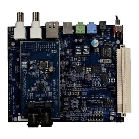
Page 8: Getting Started
ZLR964222L Line Module User Guide Getting Started The Microsemi ZLR964222L line module is designed to mate with the SM2 receptacle found on the ZTAP platform and is configurable by the MiToolkit software. Figure 1 - ZTAP and ZLR964222L Line Module Setup The ZTAP platform can accommodate one to eight telephone interfaces for the SM or DIN receptacle and up to four interfaces for the SM2 receptacle (depending on line module capability). -
Page 9: Making Test Calls
ZLR964222L Line Module User Guide Quick start steps: 1. Assemble the components as shown in Figure 1 and connect a USB cable between the ZTAP’s USB port (J7101) and a PC. 2. Plug the supplied 12V AC/DC adapter into the ZTAP’s +12 V input jack J6101. 3. - Page 10 ZLR964222L Line Module User Guide • Mini-PBX detects the telephone set going off-hook and provides a dial tone. It also shows which extension has gone off-hook. Let us assume that it is extension 100 in this example. To call the second FXS port, dial 7101 (i.e.
-
Page 11: System Description
ZLR964222L Line Module User Guide System Description Module Features The ZLR964222L line module features one Le9642 miSLIC Subscriber Line Interface Device, a programmable shared buck-boost ABS switching regulator circuit, line interface, and protection components. The Le9642 combines two-channel SLIC and SLAC functionality into a thermally-enhanced 48-QFN 7x7 mm package. The module plugs into the ZTAP board using the SM2 interface. -
Page 12: Circuit Design
ZLR964222L Line Module User Guide Circuit Design Overview The ZLR964222L Line Module consists of a Le9642 miSLIC Subscriber Line Interface Device, line interface circuit, one shared buck-boost ABS switching regulator circuit, and a host interface circuit for communication with the Microsemi ZTAP platform. This chapter highlights some of the design considerations including component selection and options. -
Page 13: Line Interface Circuit
ZLR964222L Line Module User Guide shunt resistors (RZSI1- RZSI4) and populate J1, Samtec FTSH-105-01-L-DV. This allows for cabling between the ZLR964222L Line Module and the ZSI Snooper board to manipulate the ZSI data stream. Line Interface Circuit Figure 3 below shows the ZLR964222L simplified line interface circuit. Optional components and those used for testing have been omitted. -
Page 14: Ac And Dc Sense Components
ZLR964222L Line Module User Guide Overcurrent protection is provided by the Bourns MF-SD013/250 dual PTC devices (or equivalent) which ramp to a high impedance value once the threshold current has been exceeded. Below this threshold current, the devices act as nominal 5 resistors. The hold current at 23C is 0.13 A. The MF-SD013/250 is a dual PTC that uses a polymer technology. -
Page 15: Pnp Driver
ZLR964222L Line Module User Guide voltages, usually via DC/DC converters. DC/DC converters can create switching noise on the input supply. Good decoupling is recommended. DSW3 BAV70 Populate either DSW2 (BAV23S) or DSW3/DSW4 (2x BAV70) RDS1 RPF3 VSW = 12V (10V - 14V) VBATH DSW2 CFH2... -
Page 16: High Voltage Pnp
ZLR964222L Line Module User Guide The CSW1 input capacitor for this design is a 220uF 25V low impedance electrolytic. In a customer system design, this capacitor could be reduced to a 10uF 25V X5R ceramic if there is additional bulk capacitance already in the system near the supply. -
Page 17: Single Channel Option Using Le9641 1Fxs Tracker
ZLR964222L Line Module User Guide Other Microsemi FXS devices: Le9652 2ch 150V Tracking ZSI device in a 48QFN Le9622 2ch 120V ABS device in a 53QFN Le9632 2ch 150V Tracking device in a 53QFN Le9643 1ch 95V Tracking device in a 36QFN ... -
Page 18: Figure 6 - Buck-Boost Abs To Fixed Tracking Buck-Boost Population
ZLR964222L Line Module User Guide these pins. When converting to a single channel buck-boost, all of the components on the VBL net must be upgraded to 100V rating. It may also be necessary to upgrade Q1. Observe the schematic recommendations. Addtionally, CREF1 may be changed to a 1uF 6.3V X5R (0402 minimum) ceramic capacitor when converting to a one channel design. -
Page 19: Module Configuration
ZLR964222L Line Module User Guide Module Configuration Introduction The ZLR964222L Line Module is programmed through the VoicePath Application Program Interface (VP-API-II). This API hides the complexity of the device and its internal registers and provides a much simpler interface to the software engineer. -
Page 20: Tone Profile
ZLR964222L Line Module User Guide 5.2.5 Tone Profile The MID does not include any Tone Profiles. 5.2.6 Ringing Cadence Profile The Ringing Cadence Profile sets the cadence that is associated with ringing. The default Mini-PBX ringing cadence configuration is 2 second ON and 4 seconds OFF. 5.2.7 Tone Cadence Profile The Tone Cadence Profile sets the cadence that is associated with call progress tones. -
Page 21: Profile Wizard Menu
ZLR964222L Line Module User Guide 5.3.1 Profile Wizard Menu Figure 7 below shows the Main Menu of the Profile Wizard application with the ZLR964222L project file loaded. Please note that the Tone, Cadence and Caller ID require a license to the VP-API-II and are not available with the VP-API-II Lite version. -
Page 22: Reviewing And Editing Profile Entries
ZLR964222L Line Module User Guide 5.3.2 Reviewing and Editing Profile Entries The user can edit any of the profiles by clicking on the corresponding item and can check the ones that he or she needs for the project. As an example, Figure 8 shows the contents of the Ringing Profile. -
Page 23: Figure 9 - Mini-Pbx - Configuration Mode
ZLR964222L Line Module User Guide 4. Double click on the location of the line module. It is SM CS0 on the example shown in Figure 9 below Figure 9 - Mini-PBX - Configuration Mode 5. After double clicking on the line module location, a new window will open as shown in Figure 10. -
Page 24: Performance
ZLR964222L Line Module User Guide Performance Coefficients and WinSLAC Coefficient files were generated from the Microsemi WinSLAC software and used to program filters and configure the Le9642. Microsemi provides a full set of coefficients for most world markets. 6.1.1 Coefficients The standard Profile Wizard file for ZLR964222L reference design, contains coefficient sets for the following AC profiles: AC_FXS_RF14_600R_DEF (Default narrow band 600ohm) -
Page 25: Figure 12 - Four-Wire Return Loss (Narrowband)
ZLR964222L Line Module User Guide ZLR964222L_SN_003_Ext_100 Figure 12 - Four-Wire Return Loss (Narrowband) Microsemi Corporation Confidential and Proprietary... -
Page 26: Attenuation Distortion And Gain
ZLR964222L Line Module User Guide 6.2.2 Attenuation Distortion and Gain ZLR964222L_SN_003_Ext_100 Figure 13 - Receive Path (D to A) Attenuation Distortion (Narrowband) ZLR964222L_SN_003_Ext_100 Figure 14 - Transmit Path (A to D) Attenuation Distortion (Narrowband) Microsemi Corporation Confidential and Proprietary... -
Page 27: Gain Tracking And Noise
ZLR964222L Line Module User Guide 6.2.3 Gain Tracking and Noise ZLR964222L_SN_003_Ext_100 Figure 15 - Receive Path (D to A) Gain Tracking (Narrowband) ZLR964222L_SN_003_Ext_100 Figure 16 - Transmit Path (A to D) Gain Tracking (Narrowband) Microsemi Corporation Confidential and Proprietary... -
Page 28: Total Distortion And Harmonic Distortion
ZLR964222L Line Module User Guide 6.2.4 Total Distortion and Harmonic Distortion ZLR964222L_SN_003_Ext_100 Figure 17 - Receive Path (D to A) Total Distortion (Narrowband) ZLR964222L_SN_003_Ext_100 Figure 18 - Transmit Path (A to D) Total Distortion (Narrowband) Microsemi Corporation Confidential and Proprietary... -
Page 29: Wideband Transmission Performance
ZLR964222L Line Module User Guide Wideband Transmission Performance The following graphs illustrate the wideband (150 - 6800 Hz) transmission performance using a W&G PCM-4. Note that the Le9642 device supports per-channel wideband mode. 6.3.1 Return Loss Figure 19 - Two-Wire Return Loss (Wideband) Figure 20 - Four-Wire Return Loss (Wideband) Microsemi Corporation Confidential and Proprietary... -
Page 30: Attenuation Distortion And Gain
ZLR964222L Line Module User Guide 6.3.2 Attenuation Distortion and Gain Figure 21 - Receive Path (D to A) Attenuation Distortion (Wideband) Figure 22 - Transmit Path (A to D) Attenuation Distortion (Wideband) Microsemi Corporation Confidential and Proprietary... -
Page 31: Gain Tracking And Noise
ZLR964222L Line Module User Guide 6.3.3 Gain Tracking and Noise Figure 23 - Receive Path (D to A) Gain Tracking (Wideband) Figure 24 - Transmit Path (A to D) Gain Tracking (Wideband) Microsemi Corporation Confidential and Proprietary... -
Page 32: Total Distortion And Harmonic Distortion
ZLR964222L Line Module User Guide 6.3.4 Total Distortion and Harmonic Distortion Figure 25 - Receive Path (D to A) Total Distortion (Wideband) Figure 26 - Transmit Path (A to D) Total Distortion (Wideband) Microsemi Corporation Confidential and Proprietary... -
Page 33: Power Consumption At Dc Feed And Ringing
ZLR964222L Line Module User Guide Power Consumption at DC Feed and Ringing Power Data is shown for two confurations. The first representing power consumption related to EUs Code of Conduct 2018/2019 (CoC) requirements. The second is the default profile which would be more applicable to other regions of the world. -
Page 34: Default Profile Power Consumption
ZLR964222L Line Module User Guide 4. Device power is the power dissipated in the package. Total system power must also include power delivered to the line and power efficiency of the battery supply. Total system power can be calculated (V ) + (V 6.4.2 Default Profile Power Consumption... -
Page 35: Shared Buck-Boost Abs Switching Regulator Performance
ZLR964222L Line Module User Guide Shared Buck-Boost ABS Switching Regulator Performance Input Range: 10 to 14 V Supply Efficiency: The efficiency will vary with load and input voltage. For a nominal 12 V input, the efficiency range is typically 50% to 75% Maximum Output -95 V , limited by output capacitor rating. -
Page 36: Figure 27 - Adaptive Ringing Behaviour, 0 Ren To 5Ren
ZLR964222L Line Module User Guide The adaptive ringing feature for Le9642 requires VP-API-II version 2.24.0 or later. By default the Adaptive Ringing feature is disabled. The following ZTAP CLI command enables the feature on both channels, sets the power threshold to 1.2W per channel (26 * 39mW / 2) and sets the minimum ringing voltage to 83% of the nominal ringing voltage: api so 100 -d VP_DEVICE_OPTION_ID_ADAPTIVE_RINGING 61 83 VP_ADAPT_RING_SHARED_BB_ABS Once enabled, the ringing voltage should be at its nominal voltage in open circuit and drops to its minimum if the... -
Page 37: Printed Circuit Board Documentation
ZLR964222L Line Module User Guide Printed Circuit Board Documentation Revision Information ZLR964222L Revision A0: Initial Release ZLR964222L Revision A1: Soldermask fix. ZLR964222L Revision B3: Updated BBABS supply, new layout Parts Placement Strategy The ZLR964222L Line Module is designed using a two-layer PCB to demonstrate a low cost and compact design. The design features a Le9642 miSLIC Subscriber Line Interface Device, Telcordia-compliant intra-building protection, and a 2 battery buck-boost ABS swticher. -
Page 38: Zlr964222L Line Module Schematics
ZLR964222L Line Module User Guide 1ohm resistor is placed between DVDD and AVDD and a 4.7uF ceramic cap is connected from AVDD to ground. The value of the resistor should not be increased or AVDD voltage may become degraded and out of spec. One common source of EMI is exceedingly fast edge rates on digital signals. - Page 39 ZLR964222L Line Module User Guide DESCRIPTION DATE INITIAL RELEASE 12/30/13 Removed alt DSW diodes, BBABS pop options 2/05/14 ZLR964222L 2 FXS miSLIC Reference Design RCS1 change, note cleanup. SWISZ pulldown 1/22/15 Update BBABS 6/13/16 Le9642 QFN48 ZSI 2 FXS Shared Buck-Boost ABS Reference Design Corrected connection of DSW2 and DSW3 11/4/16 RE1 = 100R...
- Page 40 ZLR964222L Line Module User Guide NOTE: ZSI USES THE PCM SIGNALS PCLK = ZCLK FS = ZSYNC Connectors Le9642 DRA = ZMOSI DXA = ZMISO ZSYNC ZSYNC ZSYNC ZCLK ZCLK ZCLK ZMISO ZMISO ZMISO ZMOSI ZMOSI ZMOSI INT0 DCLK 3.3V 3.3V AGND DOUT...
- Page 41 ZLR964222L Line Module User Guide NOTE: ZSI USES THE PCM SIGNALS PCLK = ZCLK FS = ZSYNC DRA = ZMOSI SM2 CONNECTOR DXA = ZMISO 3.3V JSM2 RVDD1 3.3V DCLK PCLK INT1 IDCS DATA DOUT INT0 DS2433S AGND RVSW1 Mount posts CON32A AGND AGND...
- Page 42 ZLR964222L Line Module User Guide 3.3V 3.3VA CVD12 3.3V 3.3VA 0.1uF VBATL_VBAT CVD1 CVIO1 CVA1 CVA2 VBATH AGND 4.7uF 0.01uF 0.01uF 0.1uF 0.1uF 4.7uF 6.3V 6.3V VBL1 VBL2 DVDD1V2 DVDHPI DVDD1 AVDD1 AVDD2 POWER Locate CVDx next to DVDD, and CVAx next to AVDD pins. RTDCA1 1Meg TDC1...
- Page 43 ZLR964222L Line Module User Guide +5V VSW Option DSW3 22uH 1.8A BAV70 Populate either DSW2 (BAV23S) or DSW3/DSW4 (2x BAV70) 75R 0603 RDS1 RPF3 CSW1 220uF 10V VSW = 12V (10V - 14V) VBATH RCS1 3.01K DSW2 CFH2 CPF4 BAV23S 1206 CFH1 0.1uF...
-
Page 44: Zlr964222L Bill Of Materials
ZLR964222L Bill of Materials Item # Quantity Part Reference Value voltage rating tolerance PCB Footprint manuf manuf # distributor distributor # note CTD1 CTD2 CRD1 CRD2 CRAC1 CRAC2 CTAC1 CTAC2 0.022uF 100V CAP0603 1 CCMP1 2.2nF CAP0402 1 CCS1 220pF CAP0402 2 CFL1, CFH1 10uF... -
Page 45: Zlr964222L Rev B0 Layout Plots
ZLR964222L Line Module User Guide ZLR964222L Rev B0 Layout Plots Plots of the layout of the ZLR964222L Line Module are provided in this section. This layout is available in Cadence Allegro .brd (V16.5) format upon request. The gerber files are also available. Figure 28 - Top Etch and Silk Screen Figure 29 - Bottom Etch and Silk Screen Microsemi Corporation Confidential and Proprietary... -
Page 46: Pcb Footprint Recommendation
ZLR964222L Line Module User Guide PCB Footprint Recommendation The Le9642 is available in a 48 pin QFN package. The package uses a center EPAD for both grounding and heat dissipation. The Microsemi 48 pin QFN package uses a non-standard narrower pin width versus a standard package. - Page 47 Information relating to products and services furnished herein by Microsemi Corporation or its subsidiaries (collectively “Microsemi”) is believed to be reliable. However, Microsemi assumes no liability for errors that may appear in this publication, or for liability otherwise arising from the application or use of any such information, product or service or for any infringement of patents or other intellectual property rights owned by third parties which may result from such application or use.
Need help?
Do you have a question about the Microsemi miSLIC Le9642 and is the answer not in the manual?
Questions and answers