Table of Contents
Advertisement
Quick Links
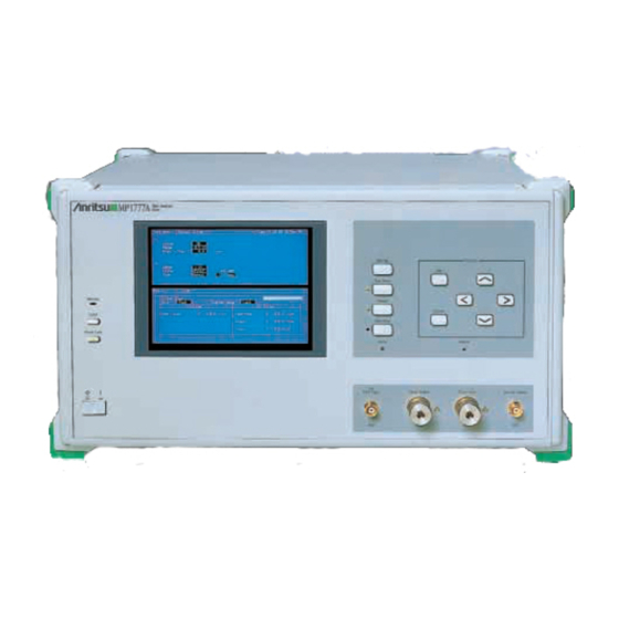
MP1777A
10 GHz Jitter Analyzer
Service Manual
Third Edition
To ensure that this equipment is used safely, important
safety items are explained in the MP1777A 10 GHz
Jitter Analyzer Operation Manual.
This manual explains important service items related
service. Read both the operation manual and this
manual, and keep both with the equipment.
ANRITSU CORPORATION
Document No.: M-W1497BE-3.0
Advertisement
Chapters
Table of Contents
Troubleshooting

Subscribe to Our Youtube Channel
Related Manuals for Anritsu MP1777A


Summary of Contents for Anritsu MP1777A
- Page 1 Service Manual Third Edition To ensure that this equipment is used safely, important safety items are explained in the MP1777A 10 GHz Jitter Analyzer Operation Manual. This manual explains important service items related service. Read both the operation manual and this manual, and keep both with the equipment.
- Page 2 Always request repair by a trained engineer who understands the hazards. Anritsu Corporation will not accept liability for any injuries sustained as a result of opening the equipment covers.
- Page 3 Part Names Part Numbers & & & & Please specify the part numbers shown in the parts list when making inquiries or when ordering parts. There may be a difference between the names of parts used in this manual and the parts actually used in the equipment or supplied for repair.
- Page 4 Power Line Fuse Protection For safety, Anritsu products have either one or two fuses in the AC power lines as requested by the customer when ordering. Single fuse: A fuse is inserted in one of the AC power lines. Double fuse: A fuse is inserted in each of the AC power lines.
-
Page 5: Table Of Contents
Table of Contents For Safety............Section 1 General........Section 2 Outline of Operation....2.1 Exchangeable Module Lists..........2.2 Block Diagram..............2.3 Module functions.............. 2-11 Section 3 Troubleshooting ......3.1 Outline................3.2 Service Kits ..............3.3 Instruments Required for Troubleshooting ...... 3.4 Overall Troubleshooting........... -
Page 7: Section 1 General
Section 1 General This service manual explains how to maintain the MP1777A 10 GHz Jitter Analyzer. Refer to the separate operation manual for handling the instruments. Our basic policy to the repair is return to the factory system, i. e. the defective instrument should be returned to Anritsu for repair. - Page 8 Section 1 General 1-2.
-
Page 9: Section 2 Outline Of Operation
Section 2 Outline of Operation Exchangeable Module Lists........Block Diagram ............Module function ............2-11... -
Page 10: Exchangeable Module Lists
Section 2 Outline of Operation Exchangeable Module Lists The MP1777A is Composed of the 24 exchangeable modules and 5 Options listed in Tables 2-1 and 2-2, respectively. Table 2-1 Exchangeable Modules of MP1777A Order No./ Model Name Product Name Remarks Mfg. - Page 11 2.1 Exchangeable Module Lists Options Table 2-2 of MP1777A Model name Name Order No. MP1777A-01 2494M/4988M/9977M Jitter 44Y104610E MP1777A-02 2666M/5332M/10664M Jitter 44Y104610B MP1777A-04 3062M/6125M/12249M Jitter 44Y104610H MP1777A-10 High sensitive input 44Y104610D MP1777A-12 1MHz HPF...
-
Page 12: Block Diagram
Section 2 Outline of Operation Block Diagram This section shows the block diagram of the MP1777A. - Page 13 Section 2 Outline of Operation TITLE DRAWNG No.
- Page 14 Section 2 Outline of Operation DRAWNG No.
- Page 15 Section 2 Outline of Operation...
- Page 16 Section 2 Outline of Operation DRAWNG No.
- Page 17 Section 2 Outline of Operation DRAWNG No.
- Page 18 Section 2 Outline of Operation DRAWNG No. 2-10...
-
Page 19: Module Functions
This module sends the data set using the front panel keys (Local, Panel Lock, Remote) to the A2 CPU module. (10) A11 CNCT This module transmits signals from A2 to H1 LCD. (11) A13 CAL (MM100132A) This is a service kit for the calibration of the MP1777A 10 GHz Jitter Analyzer. 2-11... - Page 20 Section 2 Outline of Operation (12) G1 44Z103580 Power supply unit (2 fuses) (44Z103580) G1 44Z103580 Power supply unit (1 fuse) (44Z103580B) This module provides DC power to each modules. (13) H1 LCD (Liquid crystal display) (NL6448AC20-02) This module displays the setting values and the measured result. (14) U2 UP CONVERTER (UC25100-MX-M) This module is a frequency multiplier for the Standard and Option 01 units.
-
Page 21: Section 3 Troubleshooting
Section 3 Troubleshooting Outline ............... Service Kits..............Instruments Required for Troubleshooting ....Overall Troubleshooting .......... -
Page 22: Outline
*2: Alternate cable for W82 (used for operation check and adjustment of A401/A402), Alternate cable for W70 (used for adjustment of A7) *3: Used for operation check and adjustment of A8 *4: Connection cable between Clock Output connector of the MP1777A and A13 CAL X3... -
Page 23: Instruments Required For Troubleshooting
Table 3-2 lists the instruments required for troubleshooting. Table 3-2 Instruments Required for Troubleshooting Instrument (Maker) Major Performance HP3478A (HP) AC: 250 V, DC: ±250 V Digital Multimeter MG443B (Anritsu) 10 Hz to 30 MHz Synthesizer MF2412A (Anritsu) 10 Hz to 20 GHz Frequency Counter HP8563E (HP) 30 Hz to 26.5 GHz... -
Page 24: Overall Troubleshooting
Section 3 Troubleshooting Overall Troubleshooting Figure 3-1 shows a flowchart for specifying a defective block. Confirm that cable connections are correct and the cables are not damaged. Power ON Does the FAN rotate? Fuse, Power Unit (G1), FAN MM100124A (A2 CPU), Does the buzzer sound after tuning MM100130B (A9 R-F) the power on? - Page 25 3.4 Overall Troubleshooting Does the A3 X8 (156 M CLK OUT) MM100125A (MM100162A*) (A3 CLOCK GENERATOR) operate normally? MM100126A (MM100163A*) (A401/A402 JITTER TX) Set Bit rate to 9953 M. Set Bit rate to 10664 M (12249M*). Set Jitter to OFF. Set Jitter to OFF.
- Page 26 Section 3 Troubleshooting Set Bit rates of TX and RX to 9953 Set Bit rate to 10664 M (12249M*). MM100129A (MM100166A*) Does the A8 X3 (622 M OUT) Does the A401 X4 (REF OUT) (A8 JITTER operate normally? operate normally? MEASUREMENT) DC10025-MA-M Does the A7 X1 Input operate...
-
Page 27: Section 4 Adjustment
Section 4 Adjustment Outline ............... Instruments Required for Adjustment ......A2 CPU (MM100124A) ..........4.3.1 Replacing ROM (D19, D20, D52, D101, D102) ....... 4.3.2 Setting DIP SW (S2, S3) ....... 4.3.3 Setting short terminal (X3, X4, X5, X16, X17) 4-5 A3 CLOCK GENERATOR (MM100125A* ) .... -
Page 28: Outline
Section 4 Adjustment Outline Figure 4-1 shows the entire procedure for adjustment. As shown in Figure 4-1, perform the PC-board adjustments of A3, A401/402, A5 and A8 in this sequence (Note: Adjustment of the A6/A7 Jitter Detector is performed at the Overall Adjustment.);... -
Page 29: Instruments Required For Adjustment
Table 4-1 Lists the Instruments required for adjustment. Table 4-1 Instruments Required for Adjustment Instrument (Maker) Major Performance HP3478A (HP) AC: 250 V, DC: ±250 V Digital Multimeter MG443B (Anritsu) 10 Hz to 30 MHz Synthesizer MF2412A (Anritsu) 10 Hz to 20 GHz Frequency Counter HP8563E (HP) 30 Hz to 36.5 GHz... -
Page 30: A2 Cpu (Mm100124A)
4.3.2 Setting DIP SW (S2, S3) Figure 4-3 shows the settings of the dip switches S2, S3 for various options (Standard, Option 01, Option 02, Option 04 and Option 12) of the MP1777A. RAM Clear 1 2 3 4 5 6 7 8... -
Page 31: Setting Short Terminal (X3, X4, X5, X16, X17)
4.3 A2 CPU (MM100124A) 4.3.3 Setting short terminal (X3, X4, X5, X16, X17) X3, X16, X17: Not used (Open) X4, X5: Set (short) the connection between #1 and #2 using DIC-252 (shorting terminal). -
Page 32: A3 Clock Generator
Connect W12, W13, W14, W15 and W16. Adjustment of clock re-generation section for DCS input. (1) Set Interface: Clock = Lock 2 MHz (Unbalanced) for the MP1777A setting. (2) Enter 2.048 MHz, +5.7 dBm signal to the DCS Input on the rear panel (75 Ω) using the MG443B (75 Ω). -
Page 33: A401/A402 Jitter Tx
191.39768 MHz 3 to 7 dBm Set Jitter = ON and Tx Range = 80 UI for the MP1777A setting. Observing X2 (2.488 G OUT) using a spectrum analyzer, verify that it is locked to the relevant frequency listed below. -
Page 34: A5 Jitter 10 G
Section 4 Adjustment A5 JITTER 10 G (MM100127A, MM100164A*) Check of 16-multiplication operation Connect W18. Set Jitter = OFF or Jitter = ON, Bit rate = 9953 M and Tx Range = 3200 UI. Observing X3 and X4 using a spectrum analyzer, verify that the frequency and level of the output signals are as listed below. -
Page 35: A8 Jitter Measurement
Adjustment of Local signal (X3, X5) used for Down Converter (U3, U4) (1) Set Bit rate = 9953 M for the MP1777A setting, and adjust R100 so that X3 frequency becomes equal to 622.08 MHz ±10 ppm by observing the frequency using a frequency counter. -
Page 36: Tx Overall Adjustment
(3) Insert A13 CAL (MM100132A) into the open slot present on the right side of the MP1777A, and connect a power cable between A401 X25 and A13 (4) Adjustment for Tx Ranges = 20 UI, 40 UI, 80UI (4.1) Set Bit rate = 9953 M, Jitter = ON and Tx Range = 80 UI;... - Page 37 (6) Adjustment for Tx Range = 0.5 UI (6.1) Set Bit rate = 9953 M and Tx Range = 0.5 UI. Observe the Clock Output of the MP1777A using a spectrum analyzer. Adjust A401 (MM100126A, MM100163A*) C2 and R189 (and R162 as required) so as to minimize the level at the center frequency (2nd harmonic of carrier, 19.90656 GHz) using a spectrum analyzer...
- Page 38 Section 4 Adjustment Table 4-2 Table for Setting Frequency Division Ratio MP1777A MS4630B Center Jitter Mod. Option Bit Rate Division Output UI Range Frequency Amplitude Freq. (Mbps) Ratio (dBm) (MHz) (UIp-p) (Hz) 3200 1/3840 2.592 2940 3.25 9953.28 1/96 103.68 73.5...
-
Page 39: Overall Adjustment
(Note 1: Adjustment method for the PC boards in which Option 04 is not installed at 422U17377 (Y1) (Y2).) (4.3) Set the MP1777A Bit rate = 9953 M, Tx Jitter = OFF and Rx Range = 1 UI. Set the Clock Input loss state. Then, connect the Clock Output to the Clock Input. - Page 40 Section 4 Adjustment (1) Adjust R232 so that the N6-#4 voltage becomes +Peak -0.1 Vdc. (R232-#2: center terminal is connected to N6-#4.) (2) Adjust R233 so that the N6-#10 voltage becomes -Peak +0.1 Vdc. (R233-#2: center terminal is connected to N6-#10.) (Note 2: Adjustment method for other than the PC boards of the Note 1 above.) (4.4) Set Bit rate = 9953 M, Tx Jitter = OFF and Rx Range = 1 UI.
- Page 41 (6.2) Set Bit rate = 9953 M, Jitter = ON and Tx Range = 0.5 UI for the MP1777A setting. Input and adjust a sine-wave signal level of f = 100 kHz from a synthesizer to the Ext Mod Input connector so that the displayed value of Tx AMPLITUDE (hereafter referred to as the displayed Tx value) becomes 0.3 UIp-p.
- Page 42 Section 4 Adjustment Observe the Clock Output signal using a spectrum analyzer, and sweep the frequency of the input signal to Ext Mod Input connector in the sweep-range between 100 kHz and 80 MHz. Then, change the value of each the parts described in (1) below, to maintain the sideband signal level within ±1 dB for 100 kHz level as reference in the range of 100 kHz to 80 MHz.
- Page 43 7. Adjustment of Rx frequency characteristics (A7 MM100128A) (7.1) Using the Extender (44Y104620), set A7 to adjustable state. (7.2) Connect the Clock Output to Clock Input of the MP1777A. (7.3) Set Bit rate = 9953 M, Jitter = ON, Tx Range = 0.5 UI, Rx Range = 1 UI and Filter = HP1 + LP.
- Page 44 Section 4 Adjustment (1) The frequency characteristics around f = 65 MHz must be within +3 dB for 100 kHz level as reference, when the displayed Tx value is equal to 0.15 UIp-p at f = 100 kHz. (2) The frequency characteristics around f = 80 MHz must be within –3 dB ±2 dB, when the displayed Tx value is equal to 0.5 UIp-p at f = 100 kHz.
-
Page 45: Calibration
4.10 Calibration 4.10 Calibration The automatic calibration software for the MP1777A allows the remote calibration of the displayed values using the GPIB Remote Control. The calibration procedures are listed below. (See the separate Jitter Calibration Software Operation Manual for further details. -
Page 46: Calibration For Tx Range = 20 Ui / 40 Ui
Section 4 Adjustment 4.10.2 Calibration for Tx Range = 0.5 UI Setup the equipment as shown in Figure 4-4-2. Run the Jitter Calibration Software. Fig. 4-4-2 Calibration for Tx Range = 0.5 UI 4-20... -
Page 47: Calibration For Rx
4.10 Calibration 4.10.3 Calibration for Rx Setup the equipment as shown in Figure 4-4-3. Run the Jitter Calibration Software. Fig. 4-4-3 Calibration for Rx 4-21... -
Page 48: Automatic Inspection
Section 4 Adjustment 4.11 Automatic Inspection Perform the inspection using the Automatic Inspection Software after performing the calibration described in section 4.10. Table 4-3 and Figures 4-5-1 to 4-5-5 show the inspection items and the equipment setups, respectively. (See the Automatic Inspection Software Operation Manual for further details.) Table 4-3 Setup Diagram List Measurement Title Setup... - Page 49 4.11 Automatic Inspection MP1777A MS4630B Network Analyzer Jitter Analyzer Output (A ch) Ext Mod Input Clock Input Clock Output GPIB Automatic Inspection Software Fig. 4-5-2 Transmiter/Receiver Loop-back Connection MP1777A MS4630B Network Analyzer Jitter Analyzer Output B ch x2 R TA...
- Page 50 Section 4 Adjustment Fig. 4-5-4 Spectrum Analyzer and Transmiter/Receiver Loop-back Connection Fig. 4-5-5 Spectrum Analyzer / Network Analyzer / Pulse Pattern Generator Connection 4-24.
-
Page 51: Section 5 Mechanical Configuration
Section 5 Mechanical Configuration This section shows the mechanical configuration diagrams (Figures. 5-1 to 5-5) and the replaceable parts lists (Tables 5-1 to 5-5) of the MP1777A. The numbers in Figures corresponds to those in the Tables, respectively. - Page 52 Section 5 Mechanical Configuration Table 5-1 Parts List for Outside Disassembly Description Remark Top cover Bottom cover Left side cover Right side cover Front bezel Front panel Handle Rear foot holder Both sides, 1 pair Rear foot Both sides, 1 pair Front foot holder Both sides, 1 pair Front foot...
- Page 53 Section 5 Mechanical Configuration...
- Page 54 Section 5 Mechanical Configuration...
- Page 55 Section 5 Mechanical Configuration...
- Page 56 Section 5 Mechanical Configuration...
- Page 57 Section 5 Mechanical Configuration Fig. 5-5 Module Disassembly UC25100–MX–M UP CONVERTER DC10025–MA–M DC10626–MA–M DOWN CONVERTER (DC12231–MA–M*) DOWN CONVERTER UC26106–MX–M (UC31122–MA–M*) UP CONVERTER MN2706A** U8 WIDEBAND AMPLIFIER for Option 04 ** for Option 10...
- Page 58 Section 5 Mechanical Configuration 5-8.
Need help?
Do you have a question about the MP1777A and is the answer not in the manual?
Questions and answers