Advertisement
Quick Links
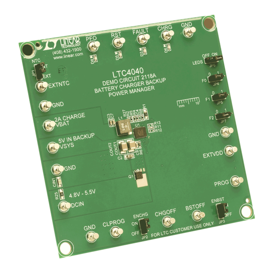
DESCRIPTION
Demonstration circuit 2118B is a combination step-down
battery charger and step-up battery backup regulator
using the
LTC
4040
monolithic system power manager.
®
The DC2118B has an input voltage range from 4.8V to
5.5V with overvoltage protection (OVP) to 40V, as limited
by the external MOSFET. The input current is monitored to
prioritize the load up to the 2.5A threshold before charge
current is reduced.
Battery Charging
As initially configured, DC2118B is programmed for 2A
charge current limit when in charge mode. The charge
voltage is jumper-selectable in 8 discrete steps from
3.45V to 3.6V for LiFePO
4
Li-ion chemistry, according to the F2/F1/F0 programming
input settings.
The charge current limit is adjustable via the PROG pin
resistor. End-of-charge status is triggered by current
falling below C/8 and indicated by the CHRG LED. The
PERFORMANCE SUMMARY
PARAMETER
Charge Mode
Input Voltage Range
Overvoltage Protection Range
Input Current Limit
Default Charging Voltage
Charging Current
Safety Timer Period
Backup Mode
DCIN Input Power Fail Threshold
System Output Voltage
Backup Battery Voltage Range
System Reset Threshold
Backup Boost Efficiency
chemistry or 3.95V to 4.1V for
Specifications are at T
DEMO MANUAL DC2118B
Battery Charger and Backup
optional NTC input provides temperature fault detection
and status indicated by the FAULT LED. Charging can be
enabled/disabled with the ENCHG jumper.
Battery Backup
Following an input power failure, the circuit automatically
shifts to battery backup boost mode to regulate the VSYS
output rail. The backup mode system output voltage is ini-
tially programmed for 5V. The input power failure status
is indicated by the PFO LED.
If VSYS ever falls below the programmed reset threshold
voltage, the RST LED will change states to indicate the
need to reset the system and recharge the battery. Backup
regulation can be enabled/disabled with the ENBST jumper.
For convenience, all LEDs can be disabled with the LED
jumper to reduce the quiescent current of the system.
Design files for this circuit board are
All registered trademarks and trademarks are the property of their respective owners.
= 25°C
A
CONDITIONS
Limited by Q1 BV
DSS
R7 = 10mΩ
F2 = 1 (Li-Ion), F1 = 1, F0 = 1
RPROG = 1.00k
F2 = 1 (Li-Ion)
F2 = 0 (LiFePO
)
4
R2 = 357k, R27 = 121k, DCIN Falling
R4 = 1.69M, R5 = 324k
R4 = 1.69M, R5 = 324k, VSYS Falling
VBAT = 3.6V, ISYS = 2A, VOUT = 5V
LTC4040
Power Manager
available.
VALUE
4.8V to 5.5V
5.5V to 40V
2.5A
4.10V
2.0A
4Hr
2Hr
4.8V
5.0V
2.7V to 5.0V
4.6V
89%
Rev. 0
1
Advertisement

Related Manuals for Linear Analog Devices LTC4040


Summary of Contents for Linear Analog Devices LTC4040
- Page 1 DEMO MANUAL DC2118B LTC4040 Battery Charger and Backup Power Manager DESCRIPTION Demonstration circuit 2118B is a combination step-down optional NTC input provides temperature fault detection battery charger and step-up battery backup regulator and status indicated by the FAULT LED. Charging can be using the 4040 monolithic system power manager.
-
Page 2: Quick Start Procedure
DEMO MANUAL DC2118B PERFORMANCE SUMMARY 2.25 BACKUP POWER 2.00 STARTED FAIL TIMER 9600mAh Li-Ion START 1.75 = 5V RPROG = 1.00k 1.50 1.25 TERMINATION 1.00 CHRG 0.75 TIMER 0.50 9600mAh Li-Ion RESTART = 5V 0.25 = 2A 0:00 0:30 1:00 1:30 2:00 2:30... - Page 3 DEMO MANUAL DC2118B QUICK START PROCEDURE 11. Total backup runtime is based on battery capacity, 2000 • V PROG circuit efficiency, and system load. Figure 2 shows PROG an example discharge curve with constant current system load. Where R = R6 = 1kΩ. PROG 12.
-
Page 4: Parts List
DEMO MANUAL DC2118B PARTS LIST ITEM REFERENCE PART DESCRIPTION MANUFACTURER/PART NUMBER Required Circuit Components CIN1 CAP ., X7R, 0.1µF, 10%, 50V, 0805 AVX, 08055C104KAT4A COUT1, COUT2 CAP ., X5R, 100µF, 20%, 10V, 1210 MURATA, GRM32ER61A107ME20L CAP ., X7R, 2.2µF, 10%, 6.3V, 0805 MURATA, GRM21BR70J225MA01L CAP ., X5R, 10µF, 20%, 10V, 0603 AVX, 0603ZD106MAT2A... -
Page 5: Schematic Diagram
DEMO MANUAL DC2118B SCHEMATIC DIAGRAM Rev. 0 Information furnished by Analog Devices is believed to be accurate and reliable. However, no responsibility is assumed by Analog Devices for its use, nor for any infringements of patents or other rights of third parties that may result from its use. Specifications subject to change without notice. - Page 6 DEMO MANUAL DC2118B ESD Caution ESD (electrostatic discharge) sensitive device. Charged devices and circuit boards can discharge without detection. Although this product features patented or proprietary protection circuitry, damage may occur on devices subjected to high energy ESD. Therefore, proper ESD precautions should be taken to avoid performance degradation or loss of functionality. Legal Terms and Conditions By using the evaluation board discussed herein (together with any tools, components documentation or support materials, the “Evaluation Board”), you are agreeing to be bound by the terms and conditions set forth below (“Agreement”) unless you have purchased the Evaluation Board, in which case the Analog Devices Standard Terms and Conditions of Sale shall govern.