Advertisement
Quick Links
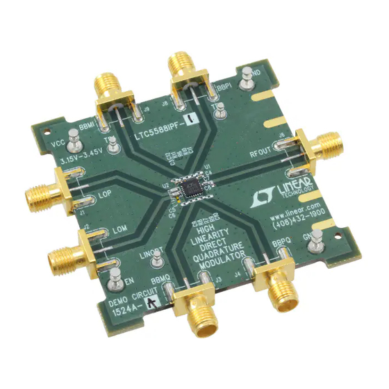
QUICK START GUIDE FOR DEMONSTRATION CIRCUIT 1524A-A
200MHZ TO 6000MHZ QUADRATURE MODULATOR WITH ULTRAHIGH OIP3
DESCRIPTION
Demonstration circuit 1524A-A is a high linearity direct
quadrature modulator featuring the LTC
The LTC5588-1 is a direct conversion I/Q modulator
designed for high performance wireless applications. It
allows direct modulation of an RF signal using differen-
tial baseband I and Q signals. It supports LTE, GSM,
EDGE, TD-SCDMA, CDMA, CDMA2000, W-CDMA, Wi-
Max and other communication standards. It can also be
configured as an image reject upconverting mixer, by
applying 90° phase-shifted signals to the I and Q inputs.
The LTC5588-1 accepts externally applied balanced I
and Q baseband input signals with a common-mode
voltage level of 0.5V. These voltage signals are con-
verted to currents and translated to RF frequency by
means of double-balanced upconverting mixers. The
mixer outputs are combined to single-ended through an
on-chip RF output balun, which also transforms the
output impedance to 50Ω for a wide RF frequency
range. A single-ended or differential LO input signal
Table 1. Typical Demo Circuit Performance Summary
T
= 25°C; V
= 3.3V, EN = 3.3V; BBPI, BBMI, BBPQ, BBMQ common-mode DC Voltage V
A
CC
1V
each (two-tone I and Q baseband input signal are at 4.5MHz and 5.5MHz), I and Q 90° shifted, lower side-band selection; P
P-P(DIFF)
f
– f
, unless otherwise noted.
LO
BB
PARAMETER
Supply Voltage
Supply Current
Sleep Current
Baseband Bandwidth
Baseband Input Current
Baseband Input Resistance
Baseband DC Common-Mode Voltage Externally Applied
Baseband Amplitude Swing
LO Match Frequency Range
RF Match Frequency Range
®
5588-1.
CONDITIONS
I
+I
, EN = High
CC1
CC2
I
+I
, EN = 0V
CC1
CC2
-1dB Bandwidth, R
= 25Ω, Single-ended
SOURCE
Single-Ended
Single-Ended
No Hard Clipping, Single-Ended
Standard Demo Board, S
< -10dB
11
Standard Demo Board, S
< -10dB
22
drives a precision quadrature phase shifter followed by
LO buffers, which in-turn drive the upconverting mix-
ers.
The LTC5588-1 offers exceptional linearity performance.
An external voltage can be applied to the LINOPT pin to
further improve its output 3rd-order intercept. The
LTC5588-1's supply voltage range is 3.15V to 3.45V,
and consumes about 303mA current.
Demonstration circuit 1524A-A is designed for evaluat-
ing the LTC5588-1 IC at RF frequencies from 700MHz
to 5GHz. With a few component changes, it can be eas-
ily optimized for evaluations at lower or higher frequen-
cies. Refer to "Application Note" section and the
LTC5588-1 data sheet for details.
Design files for this circuit board are available. Call
the LTC factory.
, LT, LTC, and LTM are registered trademarks of Linear Technology Corp.
All other trademarks are the property of their respective owners.
= 0.5V
, I and Q baseband input signal = 100kHz CW,
CMBB
DC
TYPICAL PERFORMANCE
3.15V to 3.45V
303mA
33µA
430MHz
-136µA
-3kΩ
0.5V
0.86V
P-P
600MHz to 6000MHz
700MHz to 5000MHz
LTC5588-1
= 0dBm; f
=
LOM
RF
1
Advertisement

Subscribe to Our Youtube Channel
Related Manuals for Linear 1524A-A


Summary of Contents for Linear 1524A-A
- Page 1 LTC factory. on-chip RF output balun, which also transforms the , LT, LTC, and LTM are registered trademarks of Linear Technology Corp. output impedance to 50Ω for a wide RF frequency All other trademarks are the property of their respective owners.
- Page 2 QUICK START GUIDE FOR DEMONSTRATION CIRCUIT 1524A-A 200MHZ TO 6000MHZ QUADRATURE MODULATOR WITH ULTRAHIGH OIP3 = 25°C; V = 3.3V, EN = 3.3V; BBPI, BBMI, BBPQ, BBMQ common-mode DC Voltage V = 0.5V , I and Q baseband input signal = 100kHz CW, CMBB each (two-tone I and Q baseband input signal are at 4.5MHz and 5.5MHz), I and Q 90°...
-
Page 3: Application Note
NOT be left floating to avoid damages to the LTC5588-1 IC. POWER SUPPLY CONSIDERATION In demonstration circuit 1524A-A (see Figure 3 for LO INPUT INTERFACE schematic), resistors R1 and R2 reduce the charging The standard demonstration circuit 1524A-A can accept current in the power supply bypass capacitors C1 and either single-ended or differential LO inputs. - Page 4 QUICK START GUIDE FOR DEMONSTRATION CIRCUIT 1524A-A 200MHZ TO 6000MHZ QUADRATURE MODULATOR WITH ULTRAHIGH OIP3 RF OUTPUT INTERFACE LINEARITY OPTIMIZATION Demonstration circuit 1524A-A’s RF output is single- The LTC5588-1 features a LINOPT input pin for optimiz- ended and is 50Ω matched across a wide RF frequency ing the linearity of the RF circuitry.
-
Page 5: Quick Start Procedure
QUICK START GUIDE FOR DEMONSTRATION CIRCUIT 1524A-A 200MHZ TO 6000MHZ QUADRATURE MODULATOR WITH ULTRAHIGH OIP3 QUICK START PROCEDURE Demonstration circuit 1524A-A is easy to set up to Configure the Network Analyzer for return loss evaluate the performance of the LTC5588-1. Refer to... - Page 6 QUICK START GUIDE FOR DEMONSTRATION CIRCUIT 1524A-A 200MHZ TO 6000MHZ QUADRATURE MODULATOR WITH ULTRAHIGH OIP3 OUTPUT 2ND ORDER AND 3RD ORDER INTERCEPT modulation product level at either 1893.5MHz or MEASUREMENTS (FIGURE 2) 1896.5MHz. All units are in dBm. Set the baseband signal source to provide a two- Alternatively, the output intercept can be calculated tone baseband input signal at 4.5MHz and 5.5MHz...
- Page 7 QUICK START GUIDE FOR DEMONSTRATION CIRCUIT 1524A-A 200MHZ TO 6000MHZ QUADRATURE MODULATOR WITH ULTRAHIGH OIP3 Figure 1. Proper Equipment Setup for Return Loss Measurements...
- Page 8 QUICK START GUIDE FOR DEMONSTRATION CIRCUIT 1524A-A 200MHZ TO 6000MHZ QUADRATURE MODULATOR WITH ULTRAHIGH OIP3 Figure 2. Proper Equipment Setup for RF Performance Measurements...
- Page 9 QUICK START GUIDE FOR DEMONSTRATION CIRCUIT 1524A-A 200MHZ TO 6000MHZ QUADRATURE MODULATOR WITH ULTRAHIGH OIP3 Figure 3. Demonstration Circuit Schematic...
- Page 10 Mouser Electronics Authorized Distributor Click to View Pricing, Inventory, Delivery & Lifecycle Information: Analog Devices Inc. DC1524A-A...
Need help?
Do you have a question about the 1524A-A and is the answer not in the manual?
Questions and answers