Advertisement
Quick Links
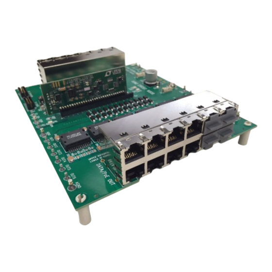
DESCRIPTION
Demonstration kit DC1843B is an 8-port Ethernet Alliance™
certified IEEE 802.3at Type 2 power sourcing equipment
(PSE) composed of a DC1842B daughter card and DC1680B
motherboard. The kit is used for evaluation of the
and
LTC4271
PSE chipset. Up to 8 powered devices (PDs)
can be connected and powered from this system using a
single power supply. A DC590 is connected to the DC1843
2
for I
C interfacing with QuikEval™. This demonstration
manual provides a Quick Start Procedure, a DC1842B
overview, a DC1680B overview, schematics, and layout
BOARD PHOTO
DEMO MANUAL DC1843B
DC1842B and DC1680B
8-Port PSE with Digital Isolation
printouts. Refer to the Layout Guide for Demonstration
Circuit 1842B when laying out the LTC4290B/LTC4271
circuit. Contact Analog Devices for this document.
LTC4290B
The DC1842B has increased surge protection over the
DC1842A. The DC1680B uses discrete Ethernet transform-
ers while the DC1680A has an integrated 12-port RJ45 jack.
Design files for this circuit board are available.
All registered trademarks and trademarks are the property of their respective owners.
LTC4290B/LTC4271
Rev B
1
Advertisement

Related Manuals for Linear Analog Devices DC1842B


Summary of Contents for Linear Analog Devices DC1842B
- Page 1 DEMO MANUAL DC1843B DC1842B and DC1680B LTC4290B/LTC4271 8-Port PSE with Digital Isolation DESCRIPTION Demonstration kit DC1843B is an 8-port Ethernet Alliance™ printouts. Refer to the Layout Guide for Demonstration certified IEEE 802.3at Type 2 power sourcing equipment Circuit 1842B when laying out the LTC4290B/LTC4271 (PSE) composed of a DC1842B daughter card and DC1680B circuit.
- Page 2 DEMO MANUAL DC1843B QUICK START PROCEDURE Demonstration kit DC1843B includes the DC1842B 3. Align pin 1 of the 30-pin male connector on the DC1842B daughter card and DC1680B motherboard. The kit is set with pin 1 of the 30-pin female connector on the DC1680B (Figure 2).
-
Page 3: Quick Start Procedure
DEMO MANUAL DC1843B QUICK START PROCEDURE (408) 432-1900 www.analog.com Figure 3. DC1843B Basic Setup Figure 4. DC1843 System Setup with the DC590, DC1680, DC1842 and 51V to 57V Power Supply Rev B... - Page 4 DEMO MANUAL DC1843B DEMONSTRATION CIRCUIT 1842B OPERATION 8-Port PSE Daughter Card with Digital Isolation proprietary dual mode 4-point detection mechanism ensur- ing excellent immunity from false PD detection. Midspan Demonstration circuit 1842B (Figure 5) features the PSEs are supported with 2-event classification and a two LTC4290B/LTC4271 chipset on a compact daughter card second backoff timer.
- Page 5 DEMO MANUAL DC1843B DEMONSTRATION CIRCUIT 1842B OPERATION Board Layout Isolation and Power Supplies Proper board layout is crucial for proper LTC4290B/ The LTC4290B/LTC4271 chipset provides communication LTC4271 chipset operation, robustness, and accuracy. across an isolation barrier through a data transformer When laying out, pay attention to parts placement, Kelvin (Figure 6).
- Page 6 DEMO MANUAL DC1843B DEMONSTRATION CIRCUIT 1842B OPERATION C Communication and Addressing AGND The LTC4271 internal registers are accessed via I C to read and/or write configuration, status, and interrupt registers. The I C lines SDAOUT, SDAIN and SCL connect to the 30-pin connector (Figure 7).
- Page 7 DEMO MANUAL DC1843B DEMONSTRATION CIRCUIT 1842B OPERATION AUTO and MID Jumpers Surge Protection The AUTO and MID pins of the LTC4271 are set by Ethernet ports can be subject to significant cable surge jumpers JP1 and JP2 respectively on the DC1842B events.
- Page 8 DEMO MANUAL DC1843B DEMONSTRATION CIRCUIT 1680B OPERATION Demonstration circuit 1680B is configured as an 8-Port, Ethernet ports. Additional pegs are placed in the last 4 pins of connector J1 to block off the unused pins when IEEE802.3at Type 1 and Type 2 PoE PSE motherboard in the DC1842B daughter card is inserted.
- Page 9 DEMO MANUAL DC1843B DEMONSTRATION CIRCUIT 1680B OPERATION MSD and RESET Pushbuttons Pushbutton switch SW2 when pressed pulls the maskable shutdown input (MSD) pin of the daughter card logic low. Pushbutton switch SW1, when pressed, pulls the RESET When pressed, all ports that have their corresponding mask pin of the daughter card logic low.
- Page 10 DEMO MANUAL DC1843B DEMONSTRATION CIRCUIT 1680B OPERATION Interrupt LED Port 1 Through 8 Power LED Indicators A red LED indicates when the INT line is pulled logic low Each PSE port has a green LED indicator to show when by the daughter card. When the interrupt is cleared (high) PoE power is present at the port.
- Page 11 DEMO MANUAL DC1843B DEMONSTRATION CIRCUIT 1843B SYSTEM DC1843B System Setup with a 14-pin ribbon cable to the DC1680B and to a PC via USB. On the PC, a GUI communicates with the board. At Figure 14 shows a basic DC1843B system setup. The the PSE output, PDs are connected.
- Page 12 DEMO MANUAL DC1843B DEMONSTRATION CIRCUIT 1842B LAYOUT Top Assembly www.analog.com Layer 1: Top Layer Rev B...
- Page 13 DEMO MANUAL DC1843B DEMONSTRATION CIRCUIT 1842B LAYOUT Layer 2: V Plane 1 Layer 3: V Plane 2 Rev B...
- Page 14 DEMO MANUAL DC1843B DEMONSTRATION CIRCUIT 1842B LAYOUT Layer 4: Bottom Layer Bottom Assembly Rev B...
- Page 15 DEMO MANUAL DC1843B DEMONSTRATION CIRCUIT 1680B LAYOUT Top Assembly (408) 432-1900 www.analog.com Rev B...
- Page 16 DEMO MANUAL DC1843B DEMONSTRATION CIRCUIT 1680B LAYOUT Layer 1: Top Layer Rev B...
- Page 17 DEMO MANUAL DC1843B DEMONSTRATION CIRCUIT 1680B LAYOUT Layer 2: AGND, CGND Plane 1 Rev B...
- Page 18 DEMO MANUAL DC1843B DEMONSTRATION CIRCUIT 1680B LAYOUT Layer 3: SIG, AGND, CGND Plane 2 Rev B...
- Page 19 DEMO MANUAL DC1843B DEMONSTRATION CIRCUIT 1680B LAYOUT Layer 4: SIG, AGND, CGND Plane 3 Rev B...
- Page 20 DEMO MANUAL DC1843B DEMONSTRATION CIRCUIT 1680B LAYOUT Layer 5: SIG, AGND, CGND Plane 4 Rev B...
- Page 21 DEMO MANUAL DC1843B DEMONSTRATION CIRCUIT 1680B LAYOUT Layer 6: Bottom Layer Rev B...
- Page 22 DEMO MANUAL DC1843B DEMONSTRATION CIRCUIT 1680B LAYOUT Bottom Assembly Rev B...
- Page 23 DEMO MANUAL DC1843B DC1842B SCHEMATIC DIAGRAM Rev B...
- Page 24 DEMO MANUAL DC1843B DC1680B SCHEMATIC DIAGRAM Rev B...
- Page 25 DEMO MANUAL DC1843B DC1680B SCHEMATIC DIAGRAM Rev B...
- Page 26 DEMO MANUAL DC1843B DC1680B SCHEMATIC DIAGRAM Rev B...
- Page 27 DEMO MANUAL DC1843B DC1680B SCHEMATIC DIAGRAM Rev B Information furnished by Analog Devices is believed to be accurate and reliable. However, no responsibility is assumed by Analog Devices for its use, nor for any infringements of patents or other rights of third parties that may result from its use. Specifications subject to change without notice.
- Page 28 DEMO MANUAL DC1843B ESD Caution ESD (electrostatic discharge) sensitive device. Charged devices and circuit boards can discharge without detection. Although this product features patented or proprietary protection circuitry, damage may occur on devices subjected to high energy ESD. Therefore, proper ESD precautions should be taken to avoid performance degradation or loss of functionality. Legal Terms and Conditions By using the evaluation board discussed herein (together with any tools, components documentation or support materials, the “Evaluation Board”), you are agreeing to be bound by the terms and conditions set forth below (“Agreement”) unless you have purchased the Evaluation Board, in which case the Analog Devices Standard Terms and Conditions of Sale shall govern.
Need help?
Do you have a question about the Analog Devices DC1842B and is the answer not in the manual?
Questions and answers