Table of Contents
Advertisement
Quick Links
www.ti.com
EVM User's Guide: TPS631012/3
TPS631012/3 Evaluation Module
Description
The TPS631012/3 is a highly efficientcy, single-
inductor, internally compensated buck-boost converter
in a 8-pin, 0.9-mm × 1.8-mm DSBGA package.
The output voltage is programmable from 1.0V to
5.5V in 25mV steps via I2C. The EVM is based
on TPS631012, in which the power-up value of
the ENABLE bit is 0. The only difference between
TPS631012 and TPS631013 is the ENABLE bit.
SLVUCQ4 – JULY 2023
Submit Document Feedback
Features
•
Output current 1.5 A (Vin > 2.7 V to Vout = 3.3V)
•
Over 92% efficiency Vin=3.6V to Vout=3.3V
Iout=1A
•
8 µA operating quiescent current
•
I2C configurable
•
Fixed frequency operation (2.0 MHz)
•
Auto PFM / Forced PWM mode selectable
TPS631012/3 EVM
Copyright © 2023 Texas Instruments Incorporated
Description
TPS631012/3 Evaluation Module
1
Advertisement
Table of Contents

Subscribe to Our Youtube Channel
Related Manuals for Texas Instruments TPS631012/3


Summary of Contents for Texas Instruments TPS631012/3
- Page 1 Description EVM User's Guide: TPS631012/3 TPS631012/3 Evaluation Module Description Features The TPS631012/3 is a highly efficientcy, single- • Output current 1.5 A (Vin > 2.7 V to Vout = 3.3V) inductor, internally compensated buck-boost converter • Over 92% efficiency Vin=3.6V to Vout=3.3V in a 8-pin, 0.9-mm ×...
-
Page 2: Kit Contents
This user’s guide describes the operation and use of the TPS631012/3EVM. The EVM is designed to help users easily evaluate and test the operation and functionality of the TPS631012/3 buck-boost converter family. The EVM has the output voltage set to 3.3 V . The output voltage can be programmed via I C interface between 1.0... - Page 3 Hardware 2 Hardware 2.1 Background The TPS631012/3EVM uses the TPS631012/3 integrated circuit (IC) , and is set to 3.3 V output voltage. The EVM operates with an input voltage between 1.6 V and 5.5 V. 2.2 Setup This section describes how to properly use the TPS631012/3EVM.
- Page 4 2.5.1 IC U1 Operation This EVM requires an appropriate I C interface, such as the TI USB2ANY, to reconfigure the TPS631012/3. The output voltage can be chosen between two I C-programmable values by using an on-board jumper. See Section for the available output voltage values.
-
Page 5: User Interface Operation
3.3.1 Home Screen The Home screen gives a short overview of the TPS631012/3 devices. To start evaluating the device, click on the Start button or on the Settings or Register Map icons on the left side of the GUI window. - Page 6 The Register Map screen shows a register-wise view of all parameters. Here, single registers can be read or written to the device (if applicable). Refer to Section 3.4 for a detailed description of the TPS631012/3 registers. Figure 3-4. GUI Register Map Screen TPS631012/3 Evaluation Module SLVUCQ4 –...
-
Page 7: Register Map
Enable short circuit hiccup protection 0 : DISABLE, 1 : ENABLE Not used CONVERTER_EN 0b0_TPS631012 Enable Converter ('AND'ed with EN-pin) 0 : DISABLE, 1 : ENABLE 0b1_TPS631013 SLVUCQ4 – JULY 2023 TPS631012/3 Evaluation Module Submit Document Feedback Copyright © 2023 Texas Instruments Incorporated... - Page 8 Defines the ramp time for the Vo soft start ramp 000: 0.256ms 001: 0.512ms 010: 1.024ms 011: 1.920ms 100: 3.584ms 101: 7.552ms 110: 9.600ms 111: 24.320ms TPS631012/3 Evaluation Module SLVUCQ4 – JULY 2023 Submit Document Feedback Copyright © 2023 Texas Instruments Incorporated...
- Page 9 INPUT VOUT VI N OUTPUT VOUT 22uF 22uF 22uF 22uF 22uF 150uF TPS631012 EXT_3V3 INPUT EXT_3V3 100k 10.0k EXT_3V3 10.0k Figure 4-1. TPS631012/3EVM Schematic SLVUCQ4 – JULY 2023 TPS631012/3 Evaluation Module Submit Document Feedback Copyright © 2023 Texas Instruments Incorporated...
-
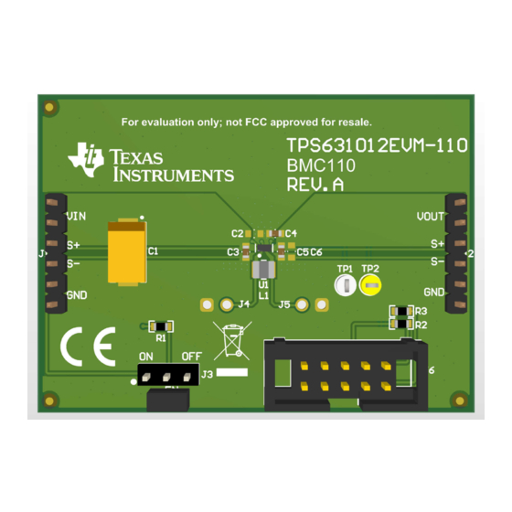
Page 10: Board Layout
PCB layout of the TPS631012/3EVM. Figure 4-2. TPS631012/3EVM PCB - Top Layer Figure 4-3. TPS631012/3EVM PCB - Bottom Layer (Top View) TPS631012/3 Evaluation Module SLVUCQ4 – JULY 2023 Submit Document Feedback Copyright © 2023 Texas Instruments Incorporated... -
Page 11: Bill Of Materials
1.5-A Output Current, High Power Density Buck- WCSP8 TPS631012 Texas Instruments Boost Converter With I2C Interface 5 Additional Information 5.1 Trademarks All trademarks are the property of their respective owners. SLVUCQ4 – JULY 2023 TPS631012/3 Evaluation Module Submit Document Feedback Copyright © 2023 Texas Instruments Incorporated... - Page 12 STANDARD TERMS FOR EVALUATION MODULES Delivery: TI delivers TI evaluation boards, kits, or modules, including any accompanying demonstration software, components, and/or documentation which may be provided together or separately (collectively, an “EVM” or “EVMs”) to the User (“User”) in accordance with the terms set forth herein.
- Page 13 www.ti.com Regulatory Notices: 3.1 United States 3.1.1 Notice applicable to EVMs not FCC-Approved: FCC NOTICE: This kit is designed to allow product developers to evaluate electronic components, circuitry, or software associated with the kit to determine whether to incorporate such items in a finished product and software developers to write software applications for use with the end product.
- Page 14 www.ti.com Concernant les EVMs avec antennes détachables Conformément à la réglementation d'Industrie Canada, le présent émetteur radio peut fonctionner avec une antenne d'un type et d'un gain maximal (ou inférieur) approuvé pour l'émetteur par Industrie Canada. Dans le but de réduire les risques de brouillage radioélectrique à...
- Page 15 www.ti.com EVM Use Restrictions and Warnings: 4.1 EVMS ARE NOT FOR USE IN FUNCTIONAL SAFETY AND/OR SAFETY CRITICAL EVALUATIONS, INCLUDING BUT NOT LIMITED TO EVALUATIONS OF LIFE SUPPORT APPLICATIONS. 4.2 User must read and apply the user guide and other available documentation provided by TI regarding the EVM prior to handling or using the EVM, including without limitation any warning or restriction notices.
- Page 16 Notwithstanding the foregoing, any judgment may be enforced in any United States or foreign court, and TI may seek injunctive relief in any United States or foreign court. Mailing Address: Texas Instruments, Post Office Box 655303, Dallas, Texas 75265 Copyright © 2023, Texas Instruments Incorporated...
- Page 17 TI products. TI’s provision of these resources does not expand or otherwise alter TI’s applicable warranties or warranty disclaimers for TI products. TI objects to and rejects any additional or different terms you may have proposed. IMPORTANT NOTICE Mailing Address: Texas Instruments, Post Office Box 655303, Dallas, Texas 75265 Copyright © 2023, Texas Instruments Incorporated...
Need help?
Do you have a question about the TPS631012/3 and is the answer not in the manual?
Questions and answers