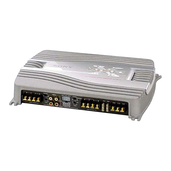
Sony XM-SD14X Service Manual
Stereo power amplifier
Hide thumbs
Also See for XM-SD14X:
- Service manual (18 pages) ,
- Service manual (18 pages) ,
- Operating instructions (2 pages)
Table of Contents
Advertisement
Quick Links
SERVICE MANUAL
Ver. 1.0 2005. 02
Sony Corporation
9-879-509-01
2005B04-1
e Vehicle Group
© 2005. 02
Published by Sony Engineering Corporation
SPECIFICATIONS
Circuit system
OTL (output transformerless) circuit
Pulse power supply
Inputs
RCA pin jacks
High level input connector
Input level adjustment range
0.3 – 6 V (RCA pin jacks),
1.2 – 12 V (High level input)
Outputs
Speaker terminals
Speaker impedance
2 – 8 Ω (stereo)
4 – 8 Ω (when used as a bridging amplifier)
Maximum outputs
Four speakers: 100 W × 4 (at 4 Ω)
Three speakers: 100 W × 2 + 250 W × 1 (at 4 Ω)
Rated outputs (supply voltage at 14.4 V)
55 W RMS × 4 (DIN 45500, 4 Ω)
Four speakers:
50 W RMS × 4 (20 Hz – 20 kHz, 0.04% THD, at 4 Ω)
60 W RMS × 4 (20 Hz – 20 kHz, 0.1% THD, at 2 Ω)
SN Ratio
100 dBA (reference: Rated output)
+0
Frequency response
5 Hz – 50 kHz (
–3
Harmonic distortion
0.005% or less (at 1 kHz, 4 Ω, 10 W)
Low-pass filter
80 Hz, –18 dB/oct
High-pass filter
80 Hz, –12 dB/oct
Power requirements
12 V DC car battery (negative ground)
Power supply voltage
10.5 – 16 V
30 A (at 4 Ω, 50 W × 4)
Current drain
Remote input : 1 mA
Dimensions
Approx. 350 × 55 × 238 mm
(w/h/d)
not incl. projecting parts and controls
Mass
Approx. 3.1 kg not incl. accessories
Supplied accessories
Mounting screws (4)
High level input cord (1)
Protection cap (1)
Design and specifications are subject to change without
notice.
XM-SD14X
dB)
STEREO POWER AMPLIFIER
AEP Model
UK Model
1
Advertisement
Table of Contents

Related Manuals for Sony XM-SD14X


Summary of Contents for Sony XM-SD14X
- Page 1 Supplied accessories Mounting screws (4) High level input cord (1) Protection cap (1) Design and specifications are subject to change without notice. STEREO POWER AMPLIFIER Sony Corporation 9-879-509-01 2005B04-1 e Vehicle Group © 2005. 02 Published by Sony Engineering Corporation...
-
Page 2: Table Of Contents
COMPONENTS IDENTIFIED BY MARK 0 OR DOTTED LINE WITH MARK 0 ON THE SCHEMATIC DIAGRAMS AND IN THE PARTS LIST ARE CRITICAL TO SAFE OPERATION. REPLACE THESE COMPONENTS WITH SONY PARTS WHOSE PART NUMBERS APPEAR AS SHOWN IN THIS MANUAL OR IN SUPPLEMENTS PUBLISHED BY SONY. -
Page 3: General
If you have any questions or problems concerning your unit that are not covered in this manual, please consult your nearest Sony dealer. Si desea realizar alguna consulta o solucionar algún problema relativos a la unidad que no se traten en este manual, póngase en contacto con el distribuidor Sony más próximo. Caution Precaución •... - Page 4 XM-SD14X Input Connections Conexiones de entrada High Level Input Connection (with Speaker Connection 1, 2 or 3) Line Input Connection (with Speaker Connection 1, 2 or 3) Conexión de entrada de alto nivel (con conexión de altavoces 1, 2 o 3) Conexión de entrada de línea...
-
Page 5: Disassembly
XM-SD14X SECTION 2 DISASSEMBLY Note : This set can be disassemble according to the following sequence. 2-1. BOTTOM PLATE (Page 5) 2-2. MAIN BOARD SECTION (Page 6) 2-3. MAIN BOARD 2-4. LED BOARD (Page 6) (Page 7) Note : Follow the disassembly procedure in the numerical order given. -
Page 6: Main Board Section
XM-SD14X 2-2. MAIN BOARD SECTION 5 screw 1 CN501 (+BTP 3 × 8) 2 three screws (+BTP 3 × 8) 3 three screws (+BTP 3 × 8) 4 three screws (+BTP 3 × 8) 6 MAIN board section After unfastening the screw, taping with the screw inserted facilitates the work. -
Page 7: Led Board
XM-SD14X SECTION 3 DIAGRAMS 2-4. LED BOARD • IC Block Diagram THIS NOTE IS COMMON FOR PRINTED WIRING BOARDS AND SCHEMATIC DIAGRAMS. (In addition to this, the necessary note is IC901 µPC494GS printed in each block.) 1 screw for schematic diagram: (+BTP 3 ×... -
Page 8: Printed Wiring Board
XM-SD14X 3-1. PRINTED WIRING BOARD MAIN BOARD D807 Q311 Q310 Q411 Q410 JW158 JW151 JW150 JW152 Q306 Q406 Q212 R378 B C E B C E R267 E C B Q412 D901 E C B Q312 Q210 Q407 Q307 R470... -
Page 9: Schematic Diagram - Amp Section
XM-SD14X 3-2. SCHEMATIC DIAGRAM — AMP SECTION — R159 R155 R158 R175 D101 Q108 Q104 R170 Q103 C152 Q110 R165 Q112 R167 R177 Q107 C151 C153 R163 Q101 R112 VR801 R113 R153 R161 CN901 IC801(1/2) C111 C154 R108 R169 R102... -
Page 10: Schematic Diagram - Power Section
XM-SD14X 3-3. SCHEMATIC DIAGRAM — POWER SECTION — • Refer to page 7 for IC Block Diagram and Waveform. (Page 9) D807 R805 C805 Q807 Q803 Q811 Q810 Q809 Q801 T901 Q911 C819 R926 D803 Q804 R810 R809 R814 Q908... -
Page 11: Exploded Views
XM-SD14X SECTION 4 EXPLODED VIEWS NOTE: • The mechanical parts with no reference • Color Indication of Appearance Parts The components identified by mark 0 or dotted line with mark number in the exploded views are not supplied. Example : 0 are critical for safety. -
Page 12: Main Board Section
XM-SD14X 4-2. MAIN BOARD SECTION not supplied not supplied not supplied Ref. No. Part No. Description Remark Ref. No. Part No. Description Remark A-1103-496-A MAIN BOARD, COMPLETE 7-685-646-79 SCREW +P 3X8 TYPE2 NON-SLIT 2-587-545-01 PANEL (FRONT) 7-682-948-01 SCREW +PSW 3X8 3-912-431-01 SCREW (+–P) -
Page 13: Electrical Parts List
XM-SD14X SECTION 5 MAIN ELECTRICAL PARTS LIST NOTE: • Due to standardization, replacements in • SEMICONDUCTORS The components identified by mark 0 or dotted line with mark the parts list may be different from the In each case, u : µ, for example: 0 are critical for safety. - Page 14 XM-SD14X MAIN Ref. No. Part No. Description Remark Ref. No. Part No. Description Remark C808 1-164-004-11 CERAMIC CHIP 0.1uF D302 8-719-801-78 DIODE 1SS184 C809 1-164-004-11 CERAMIC CHIP 0.1uF D401 8-719-801-78 DIODE 1SS184 C810 1-126-965-11 ELECT 22uF D402 8-719-801-78 DIODE 1SS184...
- Page 15 XM-SD14X MAIN Ref. No. Part No. Description Remark Ref. No. Part No. Description Remark JR34 1-216-864-11 SHORT CHIP Q412 8-729-120-28 TRANSISTOR 2SC1623-L5L6 Q801 8-729-901-04 TRANSISTOR DTA114EK < COIL > Q802 8-729-120-28 TRANSISTOR 2SC1623-L5L6 Q803 8-729-120-28 TRANSISTOR 2SC1623-L5L6 L801 1-410-396-41 FERRITE 0.45uH...
- Page 16 XM-SD14X MAIN Ref. No. Part No. Description Remark Ref. No. Part No. Description Remark R169 1-205-991-11 METAL 0.1X2 R312 1-216-045-00 RES-CHIP 1/10W R170 1-216-073-00 RES-CHIP 1/10W R313 1-216-069-00 RES-CHIP 6.8K 1/10W R171 1-216-089-11 RES-CHIP 1/10W R351 1-216-222-00 RES-CHIP 1/8W R172...
- Page 17 XM-SD14X MAIN Ref. No. Part No. Description Remark Ref. No. Part No. Description Remark R468 1-216-134-00 RES-CHIP 1/8W R937 1-216-049-11 RES-CHIP 1/10W R469 1-205-991-11 METAL 0.1X2 R938 1-216-073-00 RES-CHIP 1/10W R470 1-216-073-00 RES-CHIP 1/10W R939 1-216-085-11 RES-CHIP 1/10W R471 1-216-089-11 RES-CHIP...
- Page 18 XM-SD14X REVISION HISTORY Clicking the version allows you to jump to the revised page. Also, clicking the version at the upper right on the revised page allows you to jump to the next revised page. Ver. Date Description of Revision...
Need help?
Do you have a question about the XM-SD14X and is the answer not in the manual?
Questions and answers