Table of Contents
Advertisement
Quick Links
EVK-NINA-B3
Evaluation kit for NINA-B3 modules
User guide
Abstract
This document describes how to set up the EVK-NINA-B3 evaluation kit to evaluate NINA-B3 series
standalone Bluetooth
and the development capabilities included in the evaluation board.
UBX-17056481 - R08
C1-Public
®
5 low energy modules. It also describes the different options for debugging
www.u-blox.com
Advertisement
Table of Contents

Subscribe to Our Youtube Channel
Related Manuals for u-blox EVK-NINA-B3


Summary of Contents for u-blox EVK-NINA-B3
- Page 1 EVK-NINA-B3 Evaluation kit for NINA-B3 modules User guide Abstract This document describes how to set up the EVK-NINA-B3 evaluation kit to evaluate NINA-B3 series standalone Bluetooth ® 5 low energy modules. It also describes the different options for debugging and the development capabilities included in the evaluation board.
-
Page 2: Document Information
The information contained herein is provided “as is”. No warranty of any kind, either express or implied, is made in relation to the accuracy, reliability, fitness for a particular purpose or content of this document. This document may be revised by u-blox at any time. -
Page 3: Table Of Contents
Product description ..........................6 2.1 Overview ................................ 6 2.2 Kit includes ..............................8 2.3 Key features ..............................8 2.4 EVK-NINA-B3 block diagram ........................9 2.5 Connectors ..............................10 Setting up the evaluation board ....................11 3.1 Software and hardware preparation ..................... 11 Installing software .......................... - Page 4 EVK-NINA-B3 - User guide UART ..............................31 EEPROM support ..........................31 5.4 Additional Interfaces ..........................31 Extra memory – external Flash ...................... 32 Extra USB to UART interface ......................33 CPU trace interface .......................... 33 Appendix ..............................34 Schematics ............................34 Glossary ..............................
-
Page 5: Quick Start Guide
Follow the procedure outlined below to install the J-Link drivers needed for programming the module. 1. Connect the EVK-NINA-B3 board to your PC using the USB cable provided with the product. 2. Verify that the USB drivers are installed successfully. If the drivers do not install automatically,... -
Page 6: Product Description
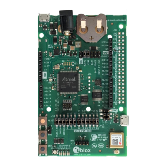
EVK-NINA-B3 - User guide Product description 2.1 Overview The EVK-NINA-B3 evaluation kit is a versatile development platform that allows quick prototyping of a variety of extreme low-power Internet of Things (IoT) applications, using full Bluetooth 5, NFC, and IEEE 802.15.4. - Page 7 EVK-NINA-B3 - User guide Figure 2: EVK-NINA-B302/-B312 evaluation board ⚠ Take care when handling the EVK-NINA-B302 or EVK-NINA-B312. Applying force to the NINA module might damage the internal antenna. Figure 3: EVK-NINA-B306/-B316 evaluation board The evaluation boards provide access to all the 38 GPIO pins and interfaces available on the NINA-B3 modules through a variety of connectors and interfaces including Arduino™...
-
Page 8: Kit Includes
• Quick start card 2.3 Key features • u-blox NINA-B3 Bluetooth low energy module based on the Nordic nRF52840 chipset Full Bluetooth 5 support NFC tag functionality 802.15.4 PHY Integrated Arm Cortex-M4 microcontroller with 1 MB flash, 256 kB RAM, and 64 MHz system clock USB 2.0... -
Page 9: Evk-Nina-B3 Block Diagram
Memory Debug Unit) Raspberry Pi 40 pin GPIO header Raspberry Pi pin NINA Open CPU function GPIO/Digital Interface UART NINA Connectivity Software function Figure 4: EVK-NINA-B3 block diagram UBX-17056481 - R08 Product description Page 9 of 40 C1-Public... -
Page 10: Connectors
CR2032 coin cell battery holder. CR2032 usually has a 3 V potential when fully charged. NFC antenna Pin header that connects to the u-blox NFC antenna included in the kit. The antenna connector can be mounted in either direction. 2.4 GHz RF antenna U.FL coaxial connector that can be used to connect antennas or RF equipment. -
Page 11: Setting Up The Evaluation Board
Plug the external power supply to the power jack connector (J5) or connect a USB host to the USB connector (J8) with a USB cable. Alternatively, you can power on a EVK-NINA-B3 evaluation board with a CR2032 coin cell battery. See also Powering options for more details. -
Page 12: Com Ports
☞ Go to the u-blox support webpage to get the latest available firmware. Instructions for reflashing the EVK-NINA-B3 can be found in the Software section of the NINA-B3 system integration manual [4]. 3.2.1.2 s-center evaluation software To enable communication with the module: 1. -
Page 13: Measuring Current Consumption
EVK-NINA-B3 - User guide 3.3 Measuring current consumption ☞ Before starting the current consumption measurement, go through the Board configuration determine which power configuration you need and what NINA signals must be isolated. The jumper connecting J22 pins 1 and 3 must be removed to measure the current consumption. - Page 14 EVK-NINA-B3 - User guide Amperemeter Voltmeter DC/DC Onboard 3.3 V supply One channel Two channels -.-- V External supply 1.7 - 3.6 V Figure 6: Current consumption measuring options UBX-17056481 - R08 Setting up the evaluation board Page 14 of 40...
-
Page 15: Board Configuration
Figure 7: Block diagram of the power net distribution Selecting the power configuration jumpers The EVK-NINA-B3 offers flexible powering options for the NINA-B3 module and the board itself. To configure this, jumpers are added or removed to pin headers, shorting two of the pins together and connecting or disconnecting different power nets on the evaluation board. - Page 16 EVK-NINA-B3 - User guide Sources Net names Targets DC/DC VDD_MCU Onboard 3.3 V PC communication converter 3V3_PI VBAT Raspberry Pi expansion board Battery VBAT_DIODE VDD_IO Battery with Board I/O power: protection diode Level shifters, LEDs etc. -.-- V Any power net...
- Page 17 EVK-NINA-B3 - User guide Table 2 describes the pinout of jumper headers J7 and J22 used to configure the board power nets. Connector Schematic Description annotation number net name Regulated 3.3 V net. This net is supplied by the board and will always be powered as long as a power source is connected.
-
Page 18: Default Power Configuration, 3.3 V
EVK-NINA-B3 - User guide Default power configuration, 3.3 V This is the default power configuration for the evaluation board, and the jumpers are installed out of the box with this power configuration. All board peripherals are powered up, the NINA module is directly supplied by the board and everything is running at 3.3 V. -
Page 19: Battery Powered, 3 - 1.7 V
EVK-NINA-B3 - User guide Battery powered, 3 – 1.7 V Figure 11 shows the default configuration for battery-powered operation, where the jumpers highlighted with dashed lines are optional. The battery voltage is connected to VDD_NINA, which in turn, is connected to the NINA-B3 VCC supply. -
Page 20: Battery Powered With Protection Diode, 2.7 - 1.7 V
EVK-NINA-B3 - User guide Battery powered with protection diode, 2.7 – 1.7 V This use case is meant to protect the battery from current back surges. When using the NFC interface, there is a risk that the applied electromagnetic field can cause back surges on the module power supply lines that typically damage a non-chargeable battery. -
Page 21: External Supply, 3.6 - 1.7 V
EVK-NINA-B3 - User guide External supply, 3.6 – 1.7 V When measuring current consumption or performing other NINA-B3 module characterization measurements, it can be useful to power the module with an external source such as a lab power supply. In such a case, all jumpers can be removed and the required supply nets can be fed externally by connecting to the pin headers. -
Page 22: Raspberry Pi Hat
EVK-NINA-B3 - User guide Raspberry Pi HAT Use the jumper configurations shown in Figure 14 to connect a HAT to the Raspberry Pi interface. Depending on how the NINA module should communicate with a test PC over USB or with the HAT, the VDD_MCU net could be left unpowered. - Page 23 EVK-NINA-B3 - User guide NINA Signal Jumper Headers Figure 15: Jumper headers J19 and J9 used to isolate specific NINA signals Table 8 describes the pinout for the jumper headers, J19 and J9, used for isolating or connecting specific evaluation board peripherals that are connected to the NINA-B3 module by default.
- Page 24 EVK-NINA-B3 - User guide Connector Pin number Schematic net name Description annotation UART_RTS_I UART to USB RTS signal GPIO_21/ NINA-B30: GPIO signal UART_CTS NINA-B31: UART CTS input UART_CTS_I UART to USB CTS signal GPIO_22/ NINA-B30: GPIO signal UART_TXD NINA-B31: UART TXD output...
-
Page 25: Interfaces And Peripherals
J19. The RGB LED shows the status for the u- connect applications. ☞ See the NINA-B3 data sheet for additional information. Table 10: EVK-NINA-B3 LED indicators UBX-17056481 - R08 Interfaces and peripherals Page 25 of 40 C1-Public... -
Page 26: Arduino Interface
EVK-NINA-B3 - User guide 5.2 Arduino interface The EVK-NINA-B3 includes a set of pin headers and mounting holes that are compatible with certain Arduino or Arduino inspired shields. Figure 17 shows the layout of the Arduino interface and Table 11 explains the pinout in more detail. -
Page 27: Arduino Shield Compatibility
Arduino shield compatibility ☞ The EVK-NINA-B3 has an I/O voltage range of 1.7–3.6 V. It can therefore be used only with shields that also support an I/O voltage within this range. The EVK-NINA-B3 has a pinout that is compatible with some Arduino, or Arduino inspired, shields. -
Page 28: Raspberry Pi Compatible Interface
5.3 Raspberry Pi compatible interface The EVK-NINA-B3 includes a 40-pin GPIO header that can be used to interface with either a Raspberry Pi computer board or with a Raspberry Pi expansion board (HAT). The EVK-NINA-B3 uses different hardware and software configurations depending on if it is connected to a Pi or a HAT; the differences are covered in this section. - Page 29 EVK-NINA-B3 - User guide Raspberry Pi Interface UART RESISTORS 3V3_PI GPIO_5 GPIO_4 GPIO_3 RASP_TXD RASP_RXD PULL-UP RESISTORS GPIO_2 GPIO_1 GPIO_52 MOUNTING HOLES GPIO_51 GPIO_50 3V3_PI GPIO_49 GPIO_48 GPIO_47 GPIO_46 GPIO_45 GPIO_44 GPIO_43 GPIO_42 GPIO_41 GPIO_40 GPIO_39 GPIO_38 GPIO_37 GPIO_36 GPIO_35...
-
Page 30: Powering Considerations
EVK-NINA-B3 - User guide Conn. Raspberry Description Schematic nRF52 Alternate functions and notes Pi pin net name GPIO23 Digital I/O GPIO_50 P0.20 Connected to NINA through a solder bridge. If the solder bridge is cut this pin is left floating. -
Page 31: Uart
NINA TX and RX pins between GPIO14 and GPIO15. If a NINA-B30 is used, this switch can also be made in the software. By default, the EVK-NINA-B3 will be configured to simulate a HAT, and GPIO14 is connected to the NINA UART_RXD pin and GPIO15 is connected to the NINA UART_TXD pin. -
Page 32: Extra Memory - External Flash
EVK-NINA-B3 - User guide Connector Schematic net name nRF52 pin Description annotation number QSPI_CS/GPIO_51 P0.17 Chip select input signal, active low QSPI_D1/GPIO_48 P0.21 MISO in single SPI mode, or data I/O signal in dual/quad mode QSPI_D2/GPIO_49 P0.22 Data I/O signal in quad mode (optional) -
Page 33: Extra Usb To Uart Interface
EVK-NINA-B3 - User guide The signals used in the QSPI interface are shared with other interfaces and GPIO functions. These have been routed both to the flash memory footprint on the bottom side of the evaluation board and to the GPIO pin header J14 (Raspberry Pi interface). To reduce the risk of interference on the QSPI interface, solder bridges have been added to the signal lines. -
Page 34: Appendix
EVK-NINA-B3 - User guide Appendix A Schematics TP35 TP38 TP27 TP16 TP19 TP18 TP15 TP17 TP12 TP14 TP13 R6 R26 TP24 TP11 TP10 TP26 Top view Bottom view (mirrored) Figure 22: Component layout UBX-17056481 - R08 Appendix Page 34 of 40... - Page 35 EVK-NINA-B3 - User guide Figure 23: NINA module schematic UBX-17056481 - R08 Appendix Page 35 of 40 C1-Public...
- Page 36 EVK-NINA-B3 - User guide Figure 24: Hub, FTDI, and flash schematic UBX-17056481 - R08 Appendix Page 36 of 40 C1-Public...
- Page 37 EVK-NINA-B3 - User guide Figure 25: Headers and buttons schematic UBX-17056481 - R08 Appendix Page 37 of 40 C1-Public...
- Page 38 EVK-NINA-B3 - User guide Figure 26: Power supply schematics UBX-17056481 - R08 Appendix Page 38 of 40 C1-Public...
-
Page 39: B Glossary
EVK-NINA-B3 - User guide B Glossary Abbreviation Definition Application programming interface Clear To send Evaluation kit Ground GPIO General-Purpose Input/Output Light-Emitting Diode Micro controller unit Mass storage device Near Field Communication U.FL Coaxial RF connector Universal serial bus Request To send... -
Page 40: Related Documents
[7] u-connectXpress user guide, UBX-16024251 GitHub repository for u-blox Open CPU modules [9] FTDI Chip home page: https://ftdichip.com/ ☞ For product change notifications and regular updates of u-blox documentation, register on our website, www.u-blox.com. Revision history Revision Date Name Comments...
Need help?
Do you have a question about the EVK-NINA-B3 and is the answer not in the manual?
Questions and answers