Table of Contents
Advertisement
Quick Links
AN11022
CLRC663 evaluation board quick start guide
Rev. 1.6 — 17 May 2023
Document Information
Information
Keywords
Abstract
Content
CLRC663, CLRC663 plus, CLEV6630A, CLEV6630B, CLRC663 evaluation board, CLRC663
customer board, CLRC663 GUI, GUI, CLRC663 Support Tool, NFC Cockpit
This document describes the CLEV6630A and CLEV6630B (CLRC663 evaluation board), and
how to use it. It describes the NFC Cockpit (Version 3.6), which allows an easy basic access to
the CLRC663 registers and EEPROM in combination with basic reader functionality.
Application note
Advertisement
Table of Contents

Related Manuals for NXP Semiconductors CLRC663


Summary of Contents for NXP Semiconductors CLRC663
- Page 1 CLRC663 GUI, GUI, CLRC663 Support Tool, NFC Cockpit Abstract This document describes the CLEV6630A and CLEV6630B (CLRC663 evaluation board), and how to use it. It describes the NFC Cockpit (Version 3.6), which allows an easy basic access to...
-
Page 2: Mcuxpresso Ide
AN11022 NXP Semiconductors CLRC663 evaluation board quick start guide Revision history Date Description 20230517 Update to latest NFC Reader Library and MCUXpresso IDE Section 7 "Radio Equipment Directive (RED)" added 20180528 Including CLEV6630A 20170515 MCUXpresso IDE installation and usage chapter added... -
Page 3: Introduction
„MIFARE DESFire card“ refers to a MIFARE DESFire IC-based contactless card. 1.1 CLRC663 registers and EEPROM concept The CLRC663 uses internal registers to adapt and optimize the functionality and performance for each of the supported protocols and data rates dependent on the connected antenna, matching network and receiver path. -
Page 4: Hardware
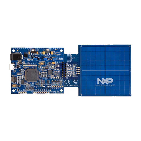
(polarity does not matter) with at least 7.5 V, since the board provides a rectifier and LDO to supply the circuit with 5 V and 3.3 V. The CLRC663 is connected to an NXP LPC1769 µC via SPI. A specific firmware on the LPC1769 allows to use the CLEV6630A / CLEV6630B together with the NFC Cockpit. - Page 5 AN11022 NXP Semiconductors CLRC663 evaluation board quick start guide Figure 2. CLEV6630B top view AN11022 All information provided in this document is subject to legal disclaimers. © 2023 NXP B.V. All rights reserved. Application note Rev. 1.6 — 17 May 2023...
-
Page 6: Schematics
AN11022 NXP Semiconductors CLRC663 evaluation board quick start guide 2.2 Schematics The complete schematics of the CLRC663 evaluation board are shown in the Figure Figure Figure Figure 7, and Figure 2.2.1 LPC1769 The CLEV6630A / CLEV6630B contains an NXP LPC1769 (see... - Page 7 AN11022 NXP Semiconductors CLRC663 evaluation board quick start guide Figure 4. JTAG interface and serial EEPROM AN11022 All information provided in this document is subject to legal disclaimers. © 2023 NXP B.V. All rights reserved. Application note Rev. 1.6 — 17 May 2023...
-
Page 8: Power Supply
As soon as the board is supplied with power, the red LED LD100 must be on. The CLRC663 evaluation board provides two LDOs, one for 5 V and one for 3.3 V. 5 V LDO is only be used, if the external power supply is connected and used (J101 default). -
Page 9: Clrc663
• J303: either VBAT = 5 V or 3.3 V (default) • J300: closed (default) or to measure the ITVDD (bridge with an ampere meter) or to supply the CLRC663 (center pin of J300) with external TVDD from external DC power supply Note: The best RF performance can be achieved with external power supply. -
Page 10: Clev6630A / Clev6630B Clrc663
AN11022 NXP Semiconductors CLRC663 evaluation board quick start guide The relevant test signals can be derived from the digital test pins at the bottom of the board and the two analog test pins AUX1 and AUX2. Figure 7. CLEV6630A / CLEV6630B CLRC663 The antenna connection uses the standard tuning circuit. - Page 11 Note: The CLRC663 plus (CLEV6630B) can drive more output power than the CLRC663 (CLEV6630A), so the antenna for the CLRC663 plus could be tuned with a lower impedance to increase the field strength. However, the maximum allowed field strength must be taken into account, too.
-
Page 12: Clev6630A / Clev6630B Default Jumper Settings
AN11022 NXP Semiconductors CLRC663 evaluation board quick start guide 2.3 Jumper settings Three jumpers can be used to evaluate the different power supply options: J101: either external or USB power supply (default) J303: either VBAT = 5 V or 3.3 V (default) -
Page 13: Clev6630A / Clev6630B Jumper Settings For External Power Supply
AN11022 NXP Semiconductors CLRC663 evaluation board quick start guide Figure 11. CLEV6630A / CLEV6630B jumper settings for external power supply AN11022 All information provided in this document is subject to legal disclaimers. © 2023 NXP B.V. All rights reserved. Application note Rev. -
Page 14: Software
The CLEV6630A / CLEV6630B evaluation board is delivered with a graphical user interface application (GUI), the NFC Cockpit. The NFC Cockpit can be used to explore the functionality of the CLRC663 and perform RF and antenna design-related tests. It allows a direct register access as well as EEPROM read and write access. - Page 15 AN11022 NXP Semiconductors CLRC663 evaluation board quick start guide Figure 12. NFC Cockpit VCOM driver CLEV6630A / CLEV6630B connected to the PC, driver properly installed. AN11022 All information provided in this document is subject to legal disclaimers. © 2023 NXP B.V. All rights reserved.
-
Page 16: Nfc Cockpit
LPC VCOM interface) is enabled automatically. Note: The NFC Cockpit is a development tool, and therefore allows many different kinds of operations, even “useless” ones at a first glance. The correct use of the NFC Cockpit is required to operate the CLRC663 properly. - Page 17 1. <Load Protocol> (e.g. type A 106) 2. <Single REQA> (using again the EEPROM settings) Note: The EEPROM of the CLRC663 is locked for all the LoadProtocol area. AN11022 All information provided in this document is subject to legal disclaimers.
-
Page 18: Clrc663 Register Access
NXP Semiconductors CLRC663 evaluation board quick start guide 3.2.1 CLRC663 register access The NFC Cockpit allows the reading and writing of all the CLRC663 registers (see Figure 15). Selecting a register reads and shows the hexadecimal content as well as the corresponding bit values. The input allows to change each bit separately as well as writing hexadecimal values. -
Page 19: Clrc663 Analog And Digital Test Signals
3.2.2 CLRC663 analog and digital test signals The NFC Cockpit allows to route the CLRC663 digital test signals to the SIGOUT pin, as well as to unlock and route the CLRC663 analog test signals to test pins AUX1 and AUX2. This is shown in Figure The digital test pin SIGOUT can be found at the J301 (pin row). -
Page 20: Clrc663 Lpcd
Otherwise the standby time can be entered and the LPCD can be started. During the LPCD being activated the CLRC663 does not react on any command, so only a detuning (-> place a card) or a Reset (press <Stop LPCD>) can end the LPCD mode. -
Page 21: Secondary Firmware Options: Emvco Loopback Application
AN11022 NXP Semiconductors CLRC663 evaluation board quick start guide 3.2.4 Secondary firmware options: EMVCo loopback application The NFC Cockpit offers the option to flash (“load”) and start applications into the LPC µC. The default application is an EMVCo loopback function, but other samples are provided within the NFC Cockpit delivery package. -
Page 22: First-Time Use
AN11022 NXP Semiconductors CLRC663 evaluation board quick start guide 4 First-time use Make sure that the LPC1769 is flashed with the correct Secondary FW (default after delivery). Check case the CLEV663 had been used with customized code before and the proper secondary firmware has to be flashed. -
Page 23: Clev6630A / Clev6630B Jumper Settings With External Tvdd
AN11022 NXP Semiconductors CLRC663 evaluation board quick start guide Figure 19. CLEV6630A / CLEV6630B jumper settings with external TVDD JP300 can be used to externally supply TVDD. AN11022 All information provided in this document is subject to legal disclaimers. © 2023 NXP B.V. All rights reserved. -
Page 24: Managing The Clrc663 Sw Projects With Mcuxpresso Ide
AN11022 NXP Semiconductors CLRC663 evaluation board quick start guide 5 Managing the CLRC663 SW projects with MCUXpresso IDE The CLRC663 SW projects are delivered in a package available through NFC Reader Library for CLRC663 product page or trough Secure Files on NXP.com https://www.nxp.com/mynxp/secure-files) in case of export controlled version. - Page 25 AN11022 NXP Semiconductors CLRC663 evaluation board quick start guide Figure 20. Checkbox for NXP debug drivers Make sure, the checkbox for installing the NXP debug drivers is activated. During the installation, the user is asked to install some required drivers. The installation of these drivers shall be accepted.
-
Page 26: Importing Provided Sw Example Projects
AN11022 NXP Semiconductors CLRC663 evaluation board quick start guide Figure 22. MCUXpresso IDE 5.3 Importing provided SW example projects The use of quick start panel provides rapid access to the most commonly used features of the MCUXpresso IDE. Quickstart panel allows easy import projects, create new projects, build, and debug projects. - Page 27 AN11022 NXP Semiconductors CLRC663 evaluation board quick start guide Figure 23. Importing project In the Quickstart panel on the left-hand side, choose “Import projects(s)”. AN11022 All information provided in this document is subject to legal disclaimers. © 2023 NXP B.V. All rights reserved.
- Page 28 AN11022 NXP Semiconductors CLRC663 evaluation board quick start guide Figure 24. Import unzipped Browse the desired package and click “Next”. AN11022 All information provided in this document is subject to legal disclaimers. © 2023 NXP B.V. All rights reserved. Application note Rev.
-
Page 29: Import Files
AN11022 NXP Semiconductors CLRC663 evaluation board quick start guide Figure 25. Import files Make sure that the option "Copy projects into workspace" is not checked. Else cross-references will be corrupted and the example projects will not compile. For a working demo project, you must import at least four subprojects. One example project, the NFC Reader Library, FreeRTOS, one chip library and one board library. - Page 30 AN11022 NXP Semiconductors CLRC663 evaluation board quick start guide Figure 26. Building the project As a part of the build output, the binary for the “User Flash” file is created. This binary file can also be used to update LPC1769 User Flash via USB mass storage interface.
-
Page 31: Running And Debugging A Project
AN11022 NXP Semiconductors CLRC663 evaluation board quick start guide 5.5 Running and debugging a project This description shows how to run the “NfcrdlibEx1_CasicDiscoveryLoop” example application for the CLEV6630A / CLEV6630B evaluation development board. The same basic principles apply for all other examples. - Page 32 AN11022 NXP Semiconductors CLRC663 evaluation board quick start guide Figure 30. Successful compile Select “LPC-Link 2” as a debug probe. AN11022 All information provided in this document is subject to legal disclaimers. © 2023 NXP B.V. All rights reserved. Application note Rev.
- Page 33 AN11022 NXP Semiconductors CLRC663 evaluation board quick start guide Figure 31. Select the launch configuration After successful software upload, the execution of the project starts immediately, but might halt at the initial breakpoint. To resume execution, click the resume button. AN11022 All information provided in this document is subject to legal disclaimers.
-
Page 34: Debug Project
AN11022 NXP Semiconductors CLRC663 evaluation board quick start guide Figure 32. Debug project In the console window, application debug outputs of the execution can be seen. Figure 33. Application printouts in console window After the execution has reached the end of the main function, click the Terminate button to stop the execution. -
Page 35: Dubug Buttons
AN11022 NXP Semiconductors CLRC663 evaluation board quick start guide Figure 34. Dubug buttons AN11022 All information provided in this document is subject to legal disclaimers. © 2023 NXP B.V. All rights reserved. Application note Rev. 1.6 — 17 May 2023 35 / 46... -
Page 36: Associated Projects
CLRC663 evaluation board quick start guide 6 Associated projects All example projects are available for download at the CLRC663 product page in the documents section and are being distributed in one single file. After downloading the zip file, unzip it and run the installer. The installer makes a copy of all documents and SW on the hard disk. -
Page 37: Discovery Loop In Poll Mode
AN11022 NXP Semiconductors CLRC663 evaluation board quick start guide 6.1 Example 1 – Basic Discovery Loop The Discovery Loop is the entry point when starting to communicate with an NFC tag or device. It scans the close environment for tags and devices of different technologies. -
Page 38: Example 2 - Advanced Discovery Loop
AN11022 NXP Semiconductors CLRC663 evaluation board quick start guide The core function of this example is “BasicDiscoveryLoop_Demo()”, where initialization of the NFC Reader library and polling for NFC technologies is implemented. After each polling loop, application is checking polling result and printout information about the detected tags or devices. -
Page 39: Example 9 - Ntag I2C
6.9 Test example 12 – CLRC663 LPCD This example is a test suite application to test CLRC663 LPCD. This test suite contains test cases for CLRC663 HAL LPCD under different conditions. Test Cases comprises of combinations of digital filter, charge pump, and detection options. -
Page 40: Simplified Api Emvco
AN11022 NXP Semiconductors CLRC663 evaluation board quick start guide Note: Not all of the offered LPCD functions might work with the used CLRC66302 (in case of using the CLEV6630A). 6.10 Simplified API EMVCo This application configures Reader Library as per EMVCo specification and start EMVCo polling. This loop back application sends SELECT_PPSE command and is used to test EMVCo.3.1a(L1) digital compliance. -
Page 41: Radio Equipment Directive (Red)
AN11022 NXP Semiconductors CLRC663 evaluation board quick start guide 7 Radio Equipment Directive (RED) The following information is provided per Article 10.8 of the Radio Equipment Directive 2014/53/EU: (a) Frequency bands in which the equipment operates. (b) The maximum RF power transmitted. -
Page 42: References
AN11019 CLRC663, MFRC630, MFRC631, SLRC610 Antenna Design Guide, AN11145 CLRC663, MFRC631, MFRC 630, SLRC610 Low-Power Card Detection AN11021 CLRC663, MFRC631, MFRC630, SLRC610 Software Design Guide for NXPRDLib 6. NFC Reader Library web pagehttp://www.nxp.com/pages/:NFC-READER-LIBRARY 7. MCUXpresso Integrated Development Environment (IDE)http://www.nxp.com/products/software-and-tools/ run-time-software/mcuxpresso-software-and-tools/mcuxpresso-integrated-development-environment-... -
Page 43: Legal Information
NXP Semiconductors. In the event that customer uses the product for design-in and use in In no event shall NXP Semiconductors be liable for any indirect, incidental, automotive applications to automotive specifications and standards, punitive, special or consequential damages (including - without limitation - customer (a) shall use the product without NXP Semiconductors’... - Page 44 AN11022 NXP Semiconductors CLRC663 evaluation board quick start guide Tables Tab. 1. Development environment ......24 Tab. 3. Characteristics ..........41 Tab. 2. Supported technologies ........38 AN11022 All information provided in this document is subject to legal disclaimers. © 2023 NXP B.V. All rights reserved.
-
Page 45: Table Of Contents
Application printouts in console window ..34 Fig. 15. CLRC663 register access ....... 18 Fig. 34. Dubug buttons ..........35 Fig. 16. CLRC663 analog and digital test signals ..19 Fig. 35. Defining RTOS preprocessor symbols .... 36 Fig. 17. CLRC663 LPCD ..........20 Fig. 36. - Page 46 3.1.2 LPC driver installation ........14 NFC Cockpit ............ 16 3.2.1 CLRC663 register access ........18 3.2.2 CLRC663 analog and digital test signals ..19 3.2.3 CLRC663 low-power card detection ....20 3.2.4 Secondary firmware options: EMVCo loopback application ........21 First-time use ............ 22 Jumper settings ..........
Need help?
Do you have a question about the CLRC663 and is the answer not in the manual?
Questions and answers