Table of Contents
Advertisement
Quick Links
Advertisement
Table of Contents

Subscribe to Our Youtube Channel
Related Manuals for Casio IT-2000


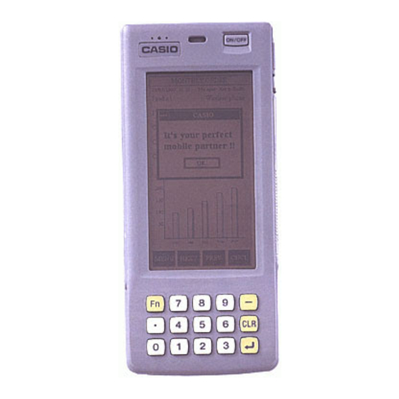
Summary of Contents for Casio IT-2000
- Page 1 SERVICE MANUAL (without price) HANDY TERMINAL IT-2000 (PX-704) JAN 1998 INDEX...
-
Page 2: Table Of Contents
CONTENTS 1. SPECIFICATIONS ....................1 1.1 CPU ......................1 1.2 Hardware ..................... 1 1.3 Memory ....................... 1 1.4 Touch Panel ....................1 1.5 Display ......................1 1.6 Sound ......................1 1.7 Key ......................1 1.8 Interface ...................... 1 1.9 PC card ....................... 2 1.10 Power supply .................... -
Page 3: Specifications
1. SPECIFICATIONS 1.1 CPU CPU: Intel 80486 GX (32 bit) Clock: 25M Hz 1.2 Hardware Configuration: IBM PC AT Architecture and dedicated hardware 1.3 Memory Main memory: 16Mbit DRAM × 2 File memory: (for D10 Model) 32Mbit NAND Flash × 1 (for D20 Model) 32Mbit NAND Flash ×... -
Page 4: Pc Card
[COM2]: 14 pin serial I/F (RS-232C) Purpose: for dedicated peripheral devices only Baud rate: 300 ~ 115,200 bps Transfer type: Start-stop synchronous transmission I/F level: SD(1) less than –5.0 V SD(0) more than +5.0 V RD(1) less than +0.6 V RD(0) more than +2.4 V Infrared (conforms to IrDA Ver. -
Page 5: Options
9-pin female) • DT-888RSC (Modular cable between IT-2060/2065IO-E and IT-2060/2065IO-E, 6-pin and 6-pin) • DT-9689AX (RS-232C 9-pin cable between IT-2000 and • SB-751HF (SCSI cable between IT-2065IO-E and PC :Centro 50-pin full male) • SB-752HH (SCSI cable between IT-2065IO-E and PC :Centro 50-pin half male) •... - Page 6 • DT-9656BCR (Touch type Bar Code Reader with built- in decoder) AC adaptor • DT-825ADP-U (120VAC, for IT-2060IO-E and IT- 2065IO-E) • DT-825ADP-G (230VAC, for IT-2060IO-E and IT- 2065IO-E) • DT-9020ADP-U (120VAC, for IT-2000) • DT-9020ADP-G (230VAC, for IT-2000) — 4 —...
-
Page 7: Interface Pin Assignment
3. INTERFACE PIN ASSIGNMENT 3.1 8 Pin serial I/F PIN No. Signal Name Description Send data Receive data Request to send Clear to send VOUT Power Ground Equipment ready Data set ready 3.2 14 Pin serial I/F (RS-232C) PIN No. Signal Name Description Ground Ground... -
Page 8: Card I/F
3.3 Card I/F 3.3.1 Memory Card Interface Memory Card Interface Signals Pin No. Signal Name I / O Description Pin No. Signal Name I / O Description 1 GND Ground 35 GND Ground 2 D3 I/O Data3 36 CD1# O Card detect1 3 D4 I/O Data4 37 D11... - Page 9 3.3.2 I/O Card Interface I/O Card Interface signals Pin No. Signal Name I / O Description Pin No. Signal Name I / O Description 1 GND Ground 35 GND Ground 2 D3 I/O Data3 36 CD1# Card detect1 3 D4 I/O Data4 37 D11 I/O Data11...
-
Page 10: System Diagram
4. SYSTEM DIAGRAM 4.1 System diagram — 8 —... -
Page 11: Block Diagram
4.2 Block diagram Battery senser Tenperature senser Illuminace senser — 9 —... -
Page 12: Pcb Diagram
ILLUMINACE SENSOR 8 pin I/F CONNECTOR RECHARGE PIN... -
Page 13: Power Supply Diagram
4.4 Power supply diagram — 11 —... -
Page 14: Circuit Description
5. CIRCUIT DESCRIPTION 5.1 Memory 5.1.1 Memory map Memory map of IT-2000 W30 model is shown in Figure 5.1.1. Figure 5.1.1 Memory map — 12 —... - Page 15 5.1.2 Memory block diagram Memory block diagram is shown in Figure 5.1.2. Figure 5.1.2 Memory block diagram — 13 —...
- Page 16 5.1.3 Serial E PROM Password and configurations data of the machine are saved in serial E PROM. PROM diagram is shown in Figure 5.1.3. Figure 5.1.3 Serial E PROM — 14 —...
-
Page 17: Kbc
5.2 KBC 5.2.1 KBC block diagram Input of matrix key and touch panel, LCD contrast, automatic backlight ON/OFF, VBAT monitoring, and buzzer are controlled at KBC. KBC diagram is shown in Figure 5.2.1. Figure 5.2.1 KBC block diagram — 15 —... - Page 18 5.2.2 Matrix key 5.2.2.1 Matrix key diagram Matrix key diagram is shown in Figure 5.2.2.1. KSENS[2:0] is connected to KEYIN#[2:0] of KBC. KSCAN[4.0] is connected to a general port of KBC. Figure 5.2.2.1 Matrix key diagram — 16 —...
- Page 19 5.2.2.2 Key Sequence Interrupt is occurred by pressing the key. When KBC acknowledges the interrupt, it starts to scan and ends after all SCANS are done once. Key sequence diagram is shown in Figure 5.2.2.2. Figure 5.2.2.2 Key Sequence — 17 —...
- Page 20 5.2.3 LCD Contrast control LCD contrast is controlled by KBC. Use a function of KBC, A/D converter to measure the temperature with a temperature sensor. Then give the measured data (10 bits AD value) to the system. According to the value system returns the contrast data to KBC.
- Page 21 5.2.4 Backlight Control Backlight is controlled by KBC. Measure the amount of light with the light sensor. When light amount falls below a certain amount backlight turns on. When light amount exceeds a certain amount backlight turns off. By having a certain amount of hysteresis it prevents the flickering of the backlight. Backlight control is shown in Figure 5.2.4.
- Page 22 5.2.5 Buzzer Control KBC controls the volume of the buzzer and the sound of a key click. Buzzer control diagram is shown in Figure 5.2.5.1. Buzzer control signal is shown in Chart 5.2.5.2. Figure 5.2.5.1 Buzzer Control block diagram Chart 5.2.5.2 Signals controlling buzzer Signal Function BZVR1...
-
Page 23: Communication
5.3 Communication Communication block diagram is shown in Figure 5.3.1. Figure 5.3.1 Communication block diagram — 21 —... -
Page 24: Pc Card
5.4 PC Card 5.4.1 Card power supply circuit The power supplied to the card is controlled by software. Card power supply circuit is shown in Figure 5.4.1. VC5ON, VC3ON, and VCC_SLOT signals control power supply ON/OFF as shown in the diagram. Figure 5.4.1 Card power supply circuit —... - Page 25 5.4.2 Card lock SW Card lock SW diagram is shown in Figure 5.4.2. Figure 5.4.2 Card lock SW diagram — 23 —...
-
Page 26: Power Supply
5.5 Power Supply 5.5.1 Power specifications Chart 4-5-1Power specifications Specification Item Name Capacity Voltage Main battery NP-500 7.2V 1300mA Backup battery CR-2032 3.0V 210mA IVR-2430 3.0V 30mA Power Supply block Name Voltage Maximum Vback 3.3V 300mA Vcore 2.4V 200mA Vsys 3.3V 300mA 5.0V... - Page 27 5.5.2 Power transition This machine is operated by rechargeable lithium battery (main battery) and coin shaped lithium battery (backup battery). When the main battery power gets low, battery replacement warning is displayed. When the main battery becomes more weak that it cannot operate the machine, system turns the power off automatically.
-
Page 28: Disassembly
6. DISASSEMBLY 6.1 Removal of the main battery and the backup batteries a M1.7 × 3.8 1 Slide the open lever to open the battery Open lever pack cover. 2 Remove the main battery. 3 Unscrew (a M1.7 × 3.8), then remove the Battery Pack backup battery cover. -
Page 29: Removal Of Sub Ass'y Pcb
5 Disconnect two cables from the connectors. 6 Remove the polyester tape. Polyester tape (Side view of 7 Remove the FPC cables by removing the connectors Adhisive Tape. FPC cable Separate the Upper Case Block and the Lower Case Block. 6.4 Removal of SUB ass’y PCB 1 Remove the connector. - Page 30 2 Separate the 8 pin serial interface connector from the Middle Case ass’y. 3 Unscrew four screws (g M2 × 10). 4 Separate the Middle Case ass’y from the Upper Case. g M2 × 10 6.5.2 Removal of the LCD ass’y 1 Unscrew two screws (h M2 ×...
-
Page 31: Disassembly Of Upper Case Block
6.5.3 Removal of the MAIN ass’y PCB 1 Pull out ejector lever. 2 Hold and remove the Ejector by pulling upward. Ejector 3 Unscrew five screws (i M2 × 4). 4 Separate the Main ass’y PCB from the Middle Case. i M2 ×... -
Page 32: Diagnostic Program
2 Copy all files in the diagnostic disk to Flash ROM card. Diagnostic disk files are listed in 7.1.4. Note: Casio Flash ROM card is recommended. If used the other card it may not work normally. 7.1.2 Boot operation 1 Set the Flash ROM card to IT-2000. - Page 33 7.1.4 Diagnostic program files Diagnostic disk files are listed bellow. [Diag] Battchk. exe 119. bat Bltest. exe Autoexec. bat Bztest.exe Config. sys Calib. exe Cardlock. exe Cardtest. exe Clktest. exe Comtest. exe Crdlswt. exe Diag_oem. mun Dinortst. exe Dispchk. exe E2ptest .exe Hwwtest.
-
Page 34: Inspection Detail
7.2 Inspection Detail Test Detail Test Menu RAM TEST Chip Select signal, Address signals, Write/Read test for DRAM DINOR FLASH Chip Select signal, Address signals, Read test for DINOR Flash NAND FLASH (except D10 Model) Chip Select signal, Address signals, Write/Read test for NAND Flash S-E2 PROM Chip Select signal, Address signals, Read test for Serial... -
Page 35: Special Tool
7.3 Special tool Special tools are necessary for 8 pin Loop test and 14 pin Loop test. 7.3.1 8 pin loop back connector 8 pin loop back connector wiring is shown in the left. Pin No Signal name 2KΩ — 33 —... - Page 36 7.3.2 14 pin I/F Tester 14 pin I/F Tester diagram is shown below.
-
Page 37: Diagnostic Test
7.4 Diagnostic test <Test Menu Display> PX-704 PX-704 PX-704 HARD TEST PROGRAM 1. RAM TEST 1. MEMORY Version 1.00 Version 1.00 Version 1.00 MEMORY Read/Write RAM TEST DISPLAY Backup Test DINOR FLASH COMM Select “1. MEMORY” NAND FLASH Select “1. RAM TEST” POWER S-E2 PROM TP &... - Page 38 PX-704 PX-704 HARD TEST PROGRAM 5. TP & KEY Version 1.00 Version 1.00 MEMORY CALIB DISPLAY TP Input COMM Select “5. TP & KEY” KEY TEST POWER TP & KEY PC CARD CLOCK Press “CLR” OTHER NAND FORMAT PX-704 6. PC CARD Version 1.00 Select “6.
- Page 39 Test menu Operation Result Fault 1. RAM TEST Display <Menu 3>. <Menu 3> 1. Read/Write 2. Backup Test Select “1. Read/Write”. RAM TEST Error RAM Testing... R/W SSSS:AAAA XX YY RAM Size = 8192K* RAM TEST --- OK Screen displays as shown SSSS :Segment Address in the right.
- Page 40 Test menu Operation Fault Result Select “9. NAND FOR- TFORMAT Version 3. 3. 3-SP MAT”. Copyright c M-Systems, Medium physical size is Note: If NAND-FLASH Boot-image size is 0 Kby is already for- – reserve unit at XXXXX It may vary a little –...
- Page 41 Test menu Operation Result Fault 5. G-RAM Display <Menu 2>. <Menu 2> 1. RAM TEST 2. DINOR FLASH 3. NAND FLASH 4. S-E2 PROM 5. G-RAM 6. HW_WINDOW 7. MASK ROM Select “5. G-RAM”. Vertical Stripes GRAM Error XXXX:YYYY AA BB Screen displays as shown XXXX :Segment Address G-RAM TEST OK...
- Page 42 Test menu Operation Result Fault Select “7. MASK ROM”. MASK ROM Testing... MASK ROM Error MASK ROM TEST - OK XXXX:YYYY AA BB Screen displays as Hit Any Key!! shown in the right. XXXX :Segment Address Goes back to Menu 2. YYYY :Offset Address :Write Data :Read Data...
- Page 43 Test menu Operation Result Fault Press “ ”. 2X patterns lined up verti- cally. Press “ ”. Checker Press “ ”. Reverse checker Press “ ”. Bars — 41 —...
- Page 44 Test menu Operation Result Fault Press “ ”. Reverse bars Press “ ”. No display Press “ ”. Black Press “ ”. No display — 42 —...
- Page 45 Test menu Operation Result Fault Press “ ”. LCD TEST ---OK Goes back to Hit Any Key!! Menu 4. 9. 8 pin Loop Connect 8 pin loop back <Menu 5> connector. * Need 8 pin 1. 8 pin Loop 2. 14pin Loop l o o p b a c k 3.
- Page 46 Test menu Operation Result Fault Select “2. 14pin loop” . COM2 LINE – COM2 CONTROL -- OK Error Message COM2 DATA - OK Screen displays as COM2 DATA - NG Hit Any Key!! shown in the right. Error Message Goes back to Menu 5. Hit Any Key!! Error Message CI ON no respond...
- Page 47 Test menu Operation Result Fault Set the transmitting ma- SIR Rcv Start SIR Rcv Start chine to “3. SIR Send” Rcv Time Out Hit Any Key!! ) Communication IrDA reception is executed. Speed :115 kbps Goes back to Menu 5. The transmitting machine may not have executed “3.
- Page 48 Test menu Operation Fault Result Battery SW OFF :cover is closed Main battery cover ON :cover is opened open/close. M–Batt OFF :undetected Main battery Low (LB0). ON :detected M–Batt OFF :undetected Main battery Low (LB1). ON :detected S–Battry OFF :undetected Backup battery ON :detected (CR2032) Low.
- Page 49 Test menu Operation Fault Result Press CLR key. Select “2. TP Input”. Goes back to Menu 8. Touch the cross point by PEN (5 points). ( 0, 0) OFF Displays each coordinate figures as you touch them. While touching, “ON” is displayed.
- Page 50 Test menu Operation Result Fault 19.PC CARD Set ATA card. (Format- <Menu 9> ted) PX-704 Display <Menu 9>. 6. PC CARD Version 1.00 1. CARD TEST 2. CARD LOCK SW Select “1. CARD TEST”. PCMCIA CARD Testing..CARD Test - OK Hit Any Key!! Goes back to Menu 9.
- Page 51 Test menu Operation Result Fault Select “7. CLOCK TEST”. 1999-12-31 23:59:57 1999-12-31 23:59:58 1999-12-31 23:59:59 2000-01-01 00:00:00 2000-01-01 00:00:01 2000-01-01 00:00:02 2000-01-01 00:00:03 CLOCK TEST --- OK Hit Any Key !! Goes back to Menu 1. 22.BUZZER TEST Display <Menu 0>. <Menu 0>...
- Page 52 Test menu Operation Result Fault 24.BL OFF Display <Menu 0>. <Menu 0> PX-704 HARD TEST PROGRAM Version 1.00 1. BUZZER TEST 2. BL ON 3. BL OFF 4. Batt Meter 5. Temp Meter 6. Bright Meter Select “3. BL OFF”. Backlight turns off.
- Page 53 Test menu Operation Result Fault 26.Temp Meter Display <Menu 0>. <Menu 0> PX-704 HARD TEST PROGRAM Version 1.00 1. BUZZER TEST 2. BL ON 3. BL OFF 4. Batt Meter 5. Temp Meter 6. Bright Meter Select “5. Temp Meter”. ===== Thermometer ===== °C Displays AD value of tem-...
- Page 54 Test menu Operation Result Fault Select “6. Bright Meter”. ===== Light Sensor ===== AD=XX Displays AD value of sensor. 100 – 90 – 70 – 60 – 50 – 40 – 30 – 20 – 10 – 0 – Light level is usually 30~50 in the office.
-
Page 55: Circuit Diagrams
8. CIRCUIT DIAGRAMS 8.1 Curcuit diagram INDEX Description Drawing No. MAIN P704-MAIN-1 C341962 C341962 CHIP_SET C341962 C341962 C341962 C341962 PCMCIA C341962 DRAM/DINOR-FLASH C341962 MASK-ROM/NAND-FLASH C341962 P704-MAIN-2 LCD_POWER/EL C341963 CONNECTOR C341963 P704-SUB PCB CONNECTER C341827 VBACK/VSYS/VCORE C341827 SUPER_CAP/VCARD C341827 VIO/V50/CHARGE C341827 RS-232C/IrDA C341827 P704-LUX... - Page 56 Description: Board No. Drawing No. P704-MAIN-1C (1/9) C341962 — 54 —...
- Page 57 (98.2~) Description: Board No. Drawing No. P704-MAIN-1C (2/9) C341962 — 55 —...
- Page 58 Description: Board No. Drawing No. CHIP_SET P704-MAIN-1C (3/9) C341962 — 56 —...
- Page 59 Description: Board No. Drawing No. P704-MAIN-1C (4/9) C341962 — 57 —...
- Page 60 Description: Board No. Drawing No. P704-MAIN-1C (5/9) C341962 — 58 —...
- Page 61 Description: Board No. Drawing No. P704-MAIN-1C (6/9) C341962 — 59 —...
- Page 62 Description: Board No. Drawing No. PCMCIA P704-MAIN-1C (7/9) C341962 — 60 —...
- Page 63 DRAM IC202 IC203 IC204 IC205 × × × × × × is mounted × × × D30P is not mounted Description: Board No. Drawing No. DRAM/DINOR-FLASH P704-MAIN-1C (8/9) C341962 — 61 —...
- Page 64 NAND-FROM IC22 IC23 IC24 × × × × × × is mounted × × is not mounted D30P IC26 is not mounted mounted only on model IC17:W30 Description: Board No. Drawing No. MASK-ROM/NAND-FLASH P704-MAIN-1C (9/9) C341962 — 62 —...
- Page 65 Description: Board No. Drawing No. LCD_POWER/EL P704-MAIN-2C (1/2) C341963 — 63 —...
- Page 66 Description: Board No. Drawing No. CONNECTOR P704-MAIN-2C (2/2) C341963 — 64 —...
- Page 67 Description: Board No. Drawing No. PCB CONNECTOR P704-SUBB (1/5) C341827 — 65 —...
- Page 68 Description: Board No. Drawing No. VBACK/VSYS/VCORE P704-SUBB (2/5) C341827 — 66 —...
- Page 69 Description: Board No. Drawing No. SUPER_CAP/VCARD P704-SUBB (3/5) C341827 — 67 —...
- Page 70 Description: Board No. Drawing No. VIO/V50/CHARGE P704-SUBB (4/5) C341827 — 68 —...
- Page 71 Description: Board No. Drawing No. RS-232C/IrDA P704-SUBB (5/5) C341827 — 69 —...
- Page 72 Description: Board No. Drawing No. LUX/ON_KEY/BUZZER/CLS P704-LUXC C442504 — 70 —...
- Page 73 Description: Board No. Drawing No. BUZZER P704-BZ C442673 — 71 —...
- Page 74 Description: Board No. Drawing No. SUPER CAPACITOR P704-CAPB C442506 — 72 —...
- Page 75 Description: Board No. Drawing No. BATTERY CONNECTOR P704-BATB C442507 — 73 —...
- Page 76 Description: Board No. Drawing No. P704-KEYB C442503 — 74 —...
-
Page 77: Exploded View
9. EXPLODED VIEW... -
Page 78: Parts List
10. PARTS LIST Notes: 1. The numbers in the item column correspond to the same numbers in exploded view. 2. MARKS: Q: Quantity used per unit R: Rank A: Essential B: Stock recommended C: Less recommended X: No stock recommended —... - Page 79 IT-2000 Item Code No. Parts Name Specification Version Middle Case Block 6541 7808 MAIN ASSY C140528*12 6541 7809 MAIN ASSY C140528*13 6541 7803 MAIN ASSY C140528*7 6541 7810 MAIN ASSY C140528*14 D30P 3122 3241 TRANS/INVERTER EBX-542C 5860 9989 SCREW 2X8 NI...
- Page 80 Item Code No. Parts Name Specification Version 2765 2188 POTENTIOMETER/CHIP EVM-3YSX50B24 3841 1526 INDUCTOR LQH3C4R7M04 IC17 2012 5883 LSI/MASK ROM D23C64000LGY815MJH W30 IC200,201,206 2105 6321 IC/MOS TC7S04FU-TE85L IC301 2105 5215 IC/MOS TC7W74FU(TE12L) 6540 0227 LCD ASSY C140527*1(HOSYU)F 6514 0300 CASE/MIDDLE C140514-1 6331 6670 SCREW A33953-3...
- Page 81 Item Code No. Parts Name Specification Version Q6,10 2259 1953 FET 2SJ203-T1B 2259 1596 FET 2SJ204-T1B Q14,39 2259 2016 FET 2SJ207-T1B Q21,22,27,57,60,62 2259 2072 FET 2SJ317NY-TR Q7-9,11,13,17-19,25, 2254 0336 FET 2SK1580-T1B 27 B Q26,32,36,37,41,42, Q44-46,48-50,58,59, Q63-65,200 Q3-5,47,51,56 2254 0266 FET 2SK1582-T1B 3632 0630 FUSE/CHIP KE10...
- Page 82 CASIO TECHNO CO.,LTD. Overseas Service Division 8-11-10, Nishi-Shinjuku Shinjuku-ku, Tokyo 160-0023, Japan...
Need help?
Do you have a question about the IT-2000 and is the answer not in the manual?
Questions and answers