Advertisement
Quick Links
Isolated Dual Channel Gate Driver
Evaluation Board User's Manual
EVBUM2817/D
Introduction
This user guide supports the evaluation board for the NCP5156x. It
should be used in conjunction with the NCP5156x and NCV5156x
datasheets as well as onsemi's application notes and technical support
team. Please visit onsemi's website at www.onsemi.com.
This document describes the proposed solution for 5 kV
isolated dual channel gate driver using the NCP51561. This user's
guide also includes information regarding operating procedures,
input/output connections, an electrical schematic, printed circuit board
(PCB) layout, and a bill of material (BOM) for each evaluation board.
These evaluation boards can be used to evaluate:
•
NCP51561xyDWR2G
•
NCV51561xyDWR2G
•
NCP51560xyDWR2G
•
NCP51563xyDWR2G
•
NCV51563xyDWR2G
Description
The NCP5156x are isolated dual−channel gate drivers
with 4.5−A/9−A source and sink peak current respectively. They are
designed for fast switching to drive power MOSFETs, and SiC
MOSFET power switches. The NCP5156x offers short and matched
propagation delays.
Two independent and 5 kV
input to each output and internal functional isolation between the two
output drivers allows a working voltage of up to 1500 VDC. This
driver can be used in any possible configurations of two low side, two
high−side switches or a half−bridge driver with programmable dead
time. An ENA/DIS pin enable or disable both outputs simultaneously
when set high or low for ENABLE or DISABLE mode respectively.
The NCP5156x offer other important protection functions such as
independent under−voltage lockout for both gate drivers and a Dead
Time adjustment function.
Key Features
•
Flexible: Dual Low−Side, Dual High−Side or Half−Bridge Gate
Driver
•
Independent UVLO Protections for Both Output Drivers
•
Output Supply Voltage from 6.5 V to 30 V with 5−V, 8−V for
MOSFET, 13−V and 17−V UVLO for SiC, Thresholds
•
4.5−A Peak Source, 9−A Peak Sink Output
•
Common Mode Transient Immunity CMTI >200 V/ns
•
Propagation Delay Typical 36 ns with
♦
5 ns Max Delay Matching per Channel
♦
5 ns Max Pulse−Width Distortion
•
User Programmable Input Logic
♦
Single or Dual−Input Modes Via ANB (NCP51561/563 only)
♦
ENABLE or DISASBLE Mode
© Semiconductor Components Industries, LLC, 2021
November, 2021 − Rev. 1
internal galvanic isolation from
RMS
EVAL BOARD USER'S MANUAL
RMS
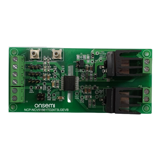
Figure 1. Evaluation Board Picture
FUNCTIONAL BLOCK DIAGRAM
V
DD
VDD UVLO
INA
INA
INB
INB
ANB
VDD
ENA/DIS
DT
GND
1
www.onsemi.com
Type−A
Type−B
Type−C
PIN CONNECTIONS
INA
VCCA
16
INB
OUTA
15
VSSA
V
14
DD
NC
13
GND
ENA/DIS
NC
12
DT
VCCB
11
ANB
OUTB
10
V
VSSB
9
DD
UVLO
[5V, 8V,
17V]
INA
Tx
Rx
LOGIC
LOGIC
Functional
Isolation
UVLO
[5V, 8V,
17V]
INB
DEAD
Tx
Rx
LOGIC
TIME
CONTROL
Publication Order Number:
EVBUM2817/D
VCCA
OUTA
VSSA
NC
NC
VCCB
OUTB
VSSB
Advertisement

Related Manuals for onsemi EVBUM2817/D


Summary of Contents for onsemi EVBUM2817/D
- Page 1 Introduction This user guide supports the evaluation board for the NCP5156x. It should be used in conjunction with the NCP5156x and NCV5156x datasheets as well as onsemi’s application notes and technical support team. Please visit onsemi’s website at www.onsemi.com. Type−A This document describes the proposed solution for 5 kV isolated dual channel gate driver using the NCP51561.
-
Page 2: Evaluation Board Operation
EVBUM2817/D Key Features (continued) • User Programmable Dead−Time • Available Package Footprint ♦ Type−A : TO−220, TO−3P, TO−247, D−PAK, and D2PAK ♦ Type−B : TO−247−4L ♦ Type−C : D2PAK−7L EVALUATION BOARD OPERATION This section describes how to operate the NCP51561... - Page 3 EVBUM2817/D Evaluation Board Jumper Setting Table 1. EVB JUMPER SETTING Default Setting Jumper Jumper Setting Options J4−INA Option1 Jumper not installed, INA/PWM signal provided by external signal and this pin is default low if left open Option1 Option2 Jumper on J4−INA−2 and J4−INA−3 set INA low Option3 Jumper on J4−INA−2 and J4−INA−1 set INA high...
- Page 4 EVBUM2817/D Bench Setup The bench setup diagram includes the function generator, (R13) between DT pin (pin6) and GND (pin4) or DT pin power supplies and oscilloscope connections. is floating (Open). • Follow the connection procedure below and use Figure 2 If using the dual input mode, should be ANB pin (PIN7) as a reference.
- Page 5 EVBUM2817/D Power−Up and Power Down Procedure Power Up 1. Could be connect VSSA pin to VSSB pin through B Should be connect switches source pins (S2A, a wire−bridge between pin 1 and pin 2 of T.P3, if and S2B) to VSSA and VSSB pins through a the Half−Bridge application is not used.
- Page 6 EVBUM2817/D Figure 4 and Figure 5 show the NCP51561 application schematic of each evaluation board to cope with various package types. DRAINA VAIN US1MFA NCP51561 VAIN VCCA VCCA VCCA PWMA VSSA 10 pF PWMB 1 mF 4.7k OUTA T.P5 10 pF...
- Page 7 EVBUM2817/D DRAINA VAIN NCP51561 US1MFA VAIN VCCA VCCA VCCA PWMA VSSA 10 pF PWMB 1 mF 4.7k OUTA T.P5 10 pF 1 nF 1 mF 0.22 mF 10 mF 5.1V T.P4 VSSA TP10 10 mF 0.22 mF T.P2 T.P4/6 ZD1/2...
- Page 8 EVBUM2817/D Electrical Specifications Table 3 show the recommended operating conditions of NCP51561 for an evaluation board. Table 3. ELECTRICAL SPECIFICATIONS Rating Symbol Unit Power Supply Voltage – Input side Power Supply Voltage – Driver side 5−V UVLO Version 8−V UVLO Version 13−V UVLO Version...
- Page 9 EVBUM2817/D Input Stage The input pins of NCP51561 is based on a TTL And we recommends an RC network is to be added on the compatible input−threshold logic that is independent of the PWM input pins, INA and INB, for reducing the impact of...
-
Page 10: Performance Of Evaluation Board
EVBUM2817/D PERFORMANCE OF EVALUATION BOARD ANB Function This section describes application guidance and operation The NCP51561 allows changing the input signal pin of the NCP51561 for an evaluation board (EVB) include key configuration by the ANB pin for user convenience. There functions. - Page 11 EVBUM2817/D Protection Function ENABLE and DISABLE Function NCP51561 provide the protection features include Enable Figure 9 shows the timing chart of ENABLE and or Disable function, and Under−Voltage Lockout (UVLO) DISABLE function. (e.g. NCP51561xA or NCP51561xB power supplies primary−side version).
- Page 12 EVBUM2817/D Under−Voltage Lockout Protection V complementary outputs from one PWM input signal on the The NCP51561 provides the Under−Voltage Lockout INA pin regardless the INB signal when the ANB pin is high. (UVLO) protection function for V in primary−side as As test result, the V UVLO turn−on and off threshold...
- Page 13 EVBUM2817/D Experimental Waveforms with Different Dead−Time DT Pin Floating or Left Open (R13 and C12 are Open) Configurations The dead−time(DT) between the outputs (OUTA and This section shows experimental test results of dead−time OUTB) of the two channels is typically around 10 ns, which control with different dead−time (DT) configuration.
- Page 14 EVBUM2817/D DT Pin Connected to R Overlap is not allowed both switches at the same time Figure 15 shown the experimental results when the when the dead time (DT) control mode. The dead−time (DT) dead−time control resistance for 100 kW.
- Page 15 EVBUM2817/D Select the Type of Output Drive There are many similarities between SiC MOSFETs and Can be selected the type of output drive for the unipolar Si MOSFETs. However, some of the challenges faced by the or negative bias as follows:...
- Page 16 EVBUM2817/D Output Driving Current Capability Figure 19 shows the experimental result of source and respectively at 25°C when the supply voltage (VCCA and sink peak currents driving capability around 4.0 A and 10 A VCCB) is applied 12 V. (a) Source Current Capability...
- Page 17 EVBUM2817/D Printed Circuit Board Figure 21 shows the photograph of the NCP51561 MOSFET load in either of the standard TO−220, TO−3P, evaluation board for the Type−A. This EVB allows for TO−247, and TO−252 (D−PAK), and TO−263 (D2PAK ) evaluation of the device with an MOSFET and SiC footprints.
- Page 18 EVBUM2817/D Figure 23 shows the photograph of the NCP51561 evaluation of the device with an MOSFET and SiC evaluation board for the Type−B. This EVB allows for MOSFET load in the standard TO−247−4L footprint. NCP51561 Figure 23. Evaluation Board Picture of Type−B (Top View) Figure 24 shows the printed circuit board layout of NCP51561 evaluation board for the Type−B.
- Page 19 EVBUM2817/D Figure 25 shows the photograph of the NCP51561 evaluation of the device with an MOSFET and SiC evaluation board board for the Type−C. This EVB allows for MOSFET load in the standard D2PAK−7L footprint. NCP51561 Figure 25. Evaluation Board Picture of Type−C (Top View) Figure 26 shows the printed circuit board layout of NCP51561 evaluation board for the Type−C.
- Page 20 EVBUM2817/D Related Product Information [1] Datasheet of NCP51561/D available on onsemi website [2] Datasheet of NCV51561/D available on onsemi website [3] Datasheet of NCP51560/D available on onsemi website [4] Datasheet of NCP51563/D available on onsemi website [5] Datasheet of NCV51563/D...
-
Page 21: Technical Support
LIMITATIONS OF LIABILITY: onsemi shall not be liable for any special, consequential, incidental, indirect or punitive damages, including, but not limited to the costs of requalification, delay, loss of profits or goodwill, arising out of or in connection with the board, even if onsemi is advised of the possibility of such damages. In no event shall onsemi’s aggregate liability from any obligation arising out of or in connection with the board, under any theory of liability, exceed the purchase price paid for the board, if any.
Need help?
Do you have a question about the EVBUM2817/D and is the answer not in the manual?
Questions and answers