
Subscribe to Our Youtube Channel
Related Manuals for Texas Instruments DAC1220EVM


Summary of Contents for Texas Instruments DAC1220EVM
- Page 1 DAC1220EVM Evaluation Module User’s Guide August 2004 Data Acquisition Products SBAU102...
-
Page 2: Important Notice
TI product or service and is an unfair and deceptive business practice. TI is not responsible or liable for any such statements. Following are URLs where you can obtain information on other Texas Instruments products and application solutions:... -
Page 3: Evm Important Notice
EVM IMPORTANT NOTICE Texas Instruments (TI) provides the enclosed product(s) under the following conditions: This evaluation kit being sold by TI is intended for use for ENGINEERING DEVELOPMENT OR EVALUATION PURPOSES ONLY and is not considered by TI to be fit for commercial use. As such, the goods being provided may not be complete in terms of required design-, marketing-, and/or manufacturing-related protective considerations, including product safety measures typically found in the end product incorporating the goods. - Page 4 EVM. Please consult the EVM User’s Guide prior to connecting any load to the EVM output. If there is uncertainty as to the load specification, please contact a TI field representative. Mailing Address: Texas Instruments Post Office Box 655303 Dallas, Texas 75265 Copyright 2004, Texas Instruments Incorporated...
-
Page 5: Read This First
SBOS099 SN74LVC1G80 Data Sheet SCES221 Additional Documentation The following document provides information regarding selected non-TI components, which may be used in the testing of the DAC1220EVM. This document is available from the corresponding manufacturer. Document Manufacturer HPA449 User’s Guide SoftBaugh, http://www.softbaugh.com... - Page 6 If you have questions regarding either the use of this evaluation module or the information contained in the accompanying documentation, please con- tact the Texas Instruments Product Information Center at (972) 644−5580 or visit the TI web site at www.ti.com.
- Page 7 Contents Contents Overview ............... . 1.1 Introduction .
- Page 8 ..........Tables 3−1. Analog Connector Pin Descriptions for the DAC1220EVM ......
- Page 9 Chapter 1 Overview The DAC1220EVM is an evaluation fixture designed for the DAC1220 20-bit delta-sigma (∆Σ) digital-to-analog data converter. The EVM is designed for prototyping and evaluation, and includes a reference circuit, an oscillator circuit, and an output buffer amplifier. Use of the output buffer amplifier is optional.
- Page 10 The DAC1220EVM is designed using a simple card format developed by TI. This simple, consistent design makes the DAC1220EVM very easy to connect to your own prototype system. One can even think of the DAC1220EVM as an alternate package for the DAC1220—one much larger than the device itself, but also much easier to wire up by hand on a test bench.
- Page 11 These jumpers allow the current of each supply to be measured independently. 1.4 Controls The DAC1220EVM is configured using two slide switches. (See Figure 3−7 for the location of these switches.) Switch S2 selects the system clock source for the DAC1220. You can select from the 2.4576MHz crystal or an external clock.
- Page 12 Setting Up 1.5 Setting Up The way that one configures the DAC1220EVM depends on how it will be used. Consequently, there is no one single procedure to follow for setting up the DAC1220EVM. Nevertheless, it is useful to remember the following points when you are con-...
-
Page 13: Circuit Description
Circuit Description This chapter describes the DAC1220EVM circuit design in detail. The DAC1220EVM is designed to conform to TI’s Modular EVM System. It contains only those parts of the circuit that will typically be used in an applica- tion immediately surrounding the DAC1220EVM. This includes:... - Page 14 For 20-bit resolution, larger ca- pacitors are used; these give a slower settling time but generate lower noise. The DAC1220EVM is shipped with the recommended capacitor values for 20-bit mode as given in the product data sheet. If 16-bit operation is desired, the capacitors can easily be removed and replaced because they are mounted to large (0805) surface-mount footprints.
-
Page 15: Clock Oscillator
Clock Oscillator 2.2 Clock Oscillator The DAC1220EVM can be used with its on-board 2.4576MHz crystal or with an external clock source. A commonly-available crystal type in a through-hole HC49 package was used. Selector switch S2 is inserted between the crystal and the DAC. The double- pole switch disconnects the crystal from the device entirely, to better simulate actual application conditions when using an external clock. - Page 16 DAC1220 continuous-time reconstruction filter, and has a relatively weak output drive capability. For some loads, a buffer is needed. The buffer used on the DAC1220EVM is a unity-gain connected OPA335. This device, which is also used in the voltage reference circuit, offers extremely low voltage drift thanks to its auto-zeroing circuit.
- Page 17 Chapter 3 Usage This chapter describes how to use the DAC1220EVM. It also describes the switches, jumpers, and connectors on the EVM in detail. Topic Page I/O Connectors and Testpoints ....... . .
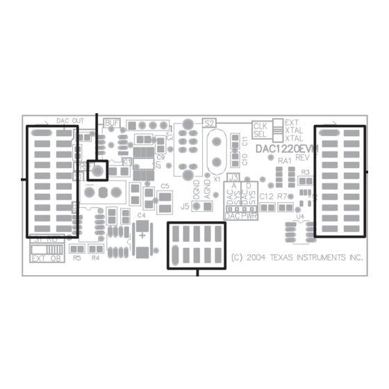
- Page 18 The positions and functions of the connectors and testpoints are shown in Figure 3−1. Figure 3−1. DAC1220EVM Connectors and Testpoints Many of the pins on the connectors are not used. On the pinout diagrams in this user’s guide, unused pins are not marked. In the pin description tables, unused pins are not listed, and ground pins are listed together, with the excep- tion of the power connector.
- Page 19 GND 1 DACOUT GND 3 BUFOUT GND 9 GND 11 GND 13 GND 17 GND 19 SYSREF Table 3−1. Analog Connector Pin Descriptions for the DAC1220EVM Standard Connection Name Name Direction Function to DAC1220 AN0− AN0− Output Signal ground for unbuffered output...
- Page 20 SDO, MOSI, or MISO, and an input line, typically called SDI, MISO, or SOMI. To more easily support these interfaces, the DAC1220EVM includes a tristate buffer connected to the serial connector in- put line. The buffer can be enabled and disabled using pin 9 on the serial con- nector;...
- Page 21 DAC1220EVM uses a single ground plane. The mother- board may have separate ground domains on AGND and DGND. The DAC1220EVM takes its ground connection from AGND. You can connect DGND to AGND on the DAC1220EVM using jumper J5, as described in sec- tion 3.2.2. 3.1.4 Testpoints There is one testpoint on the board;...
- Page 22 J3: DAC1220 Supply Current Measurement Jumpers Jumper block J3 is shown in Figure 3−6. Figure 3−6. Jumper Block J3 on the DAC1220EVM This jumper block can be used to measure the current drawn by the DAC1220 power supplies. For normal operation, when not measuring current, place shorting blocks across both jumper positions in the block.
- Page 23 The DAC1220EVM uses a single-ended reference voltage; J1, pin 18 is not connected. The external reference is filtered on board with a 1µf MLC capacitor. It may be useful to apply a larger filtering capacitor at the voltage source.
-
Page 24: Schematic And Layout
Chapter 4 Schematic and Layout This chapter contains the complete bill of materials, schematic, and PCB lay- out for the DAC1220EVM. Note: Board layouts are not to scale. These are intended to show how the board is laid out; they are not intended to be used for manufacturing DAC1220EVM PCBs. - Page 25 Schematic 4.1 Schematic Figure 4−1. Schematic DAC1220EVM XTALIN...
-
Page 26: Board Layout
Board Layout 4.2 Board Layout Figure 4−2. DAC1220EVM—Layer 1 (Top) Figure 4−3. DAC1220EVM—Layer 2 (Bottom side, viewed from top) Schematic and Layout... -
Page 27: Bill Of Materials
1µF 16V X5R 10% ceramic chip resistor C1608X5R1C105K 1µF 16V X7R 10% ceramic chip resistor C3216X7R1C226M C8, C9, C3 10µF 6.3V X5R 20% ceramic chip resistor C2012X5R0J106M Operational amplifier Texas Instruments OPA335AID Digital-to-analog converter Texas Instruments DAC1220E Tri-state buffer Texas Instruments SN74AHCT1G125DBV... -
Page 28: Texas Instruments
Mouser Electronics Authorized Distributor Click to View Pricing, Inventory, Delivery & Lifecycle Information: Texas Instruments DAC1220EVM...
Need help?
Do you have a question about the DAC1220EVM and is the answer not in the manual?
Questions and answers