Table of Contents
Advertisement
Quick Links
P6900 Series
xx
High-Density Logic Analyzer Probes
with D-Max™ Probing Technology
ZZZ
Instruction Manual
Warning
The servicing instructions are for use by qualified personnel
only. To avoid personal injury, do not perform any servicing
unless you are qualified to do so. Refer to all safety summaries
prior to performing service.
www.tektronix.com
*P077152806*
077-1528-06
Advertisement
Table of Contents

Related Manuals for Tektronix P6900 Series


Summary of Contents for Tektronix P6900 Series
- Page 1 P6900 Series High-Density Logic Analyzer Probes with D-Max™ Probing Technology Instruction Manual Warning The servicing instructions are for use by qualified personnel only. To avoid personal injury, do not perform any servicing unless you are qualified to do so. Refer to all safety summaries prior to performing service.
- Page 2 Copyright © Tektronix. All rights reserved. Licensed software products are owned by Tektronix or its subsidiaries or suppliers, and are protected by national copyright laws and international treaty provisions. Tektronix products are covered by U.S. and foreign patents, issued and pending. Information in this publication supersedes that in all previously published material.
- Page 3 Tektronix, with shipping charges prepaid. Tektronix shall pay for the return of the product to Customer if the shipment is to a location within the country in which the Tektronix service center is located. Customer shall be responsible for paying all shipping charges, duties, taxes, and any other charges for products returned to any other locations.
-
Page 5: Table Of Contents
Perform the functional check ................Inspect and clean the probes ................. Service strategy ....................Legacy probe and attachment support ..............Repackaging instructions ..................Replaceable parts ....................Parts ordering information ................... Replaceable parts list ..................Index P6900 Series Logic Analyzer Probes Instruction Manual... - Page 6 Figure 31: P6960/P6960HS single-ended PCB footprint pinout detail........Figure 32: P6962 single-ended PCB footprint pinout detail..........Figure 33: P6964 single-ended PCB footprint pinout detail..........Figure 34: P6980 differential PCB footprint pinout detail............ Figure 35: P6982 differential PCB footprint pinout detail............ P6900 Series Logic Analyzer Probes Instruction Manual...
- Page 7 Figure 39: P6962 High-Density probe accessories ............Figure 40: P6964 High-Density probe accessories ............Figure 41: P6980 High-Density Differential probe accessories ..........Figure 42: P6982 High-Density Differential probe accessories ..........Figure 43: Optional accessories.................. P6900 Series Logic Analyzer Probes Instruction Manual...
- Page 8 Table 15: P6960HS replaceable parts list ............... Table 16: P6962 replaceable parts list................Table 17: P6964 replaceable parts list................Table 18: P6980 replaceable parts list................Table 19: P6982 replaceable parts list................Table 20: P6900 Series Probes optional accessories............P6900 Series Logic Analyzer Probes Instruction Manual...
-
Page 9: Preface
Preface This document provides information on using and servicing the P6900 Series logic analyzer probes. Related documentation The following list and table provide information on the related documentation available for your Tektronix product. For additional information, refer to the Tektronix Web site (www.tektronix.com/manuals). -
Page 10: Environmental Considerations
PCB and the probe input circuitry. Compression Footprint A connectorless, solderless contact between your PCB and the P6900 Series probes. Connection is obtained by applying pressure between your PCB and the probe through a cLGA c-spring. -
Page 11: Figure I: Differential Input Amplitude
Amplitude Definition Figure i: Differential input amplitude D-Max probing technology Trademark name that describes the technology used in the P6900 Series high-density logic analyzer probes. Flying Lead Set A lead set designed to attach to a P6960 Probe to provide general-purpose probing capability. -
Page 12: Figure Iii: Probe Example
SMT KlipChip An interface device for attaching logic analyzer probes to components with a maximum lead diameter of 2.413 mm (0.095 in) and stackable on lead centers of 1.27 mm (0.050 in). viii P6900 Series Logic Analyzer Probes Instruction Manual... -
Page 13: Operating Basics
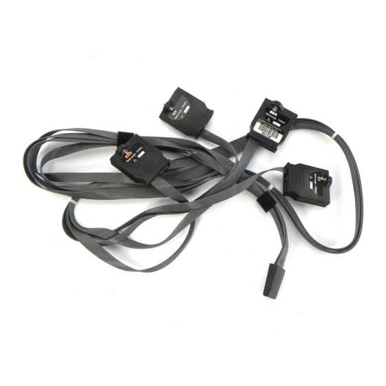
Operating basics This section provides a brief description of the Tektronix P6900 Series High-Density Logic Analyzer Probes, information on attaching color-coded probe labels, and probe and adapter connection instructions from the logic analyzer to the target system. Product description The P6900 Series Probes connect TLA7ACx Series Logic Analyzer modules to a target system. -
Page 14: Figure 1: P6960 High-Density Probe With D-Max Probing Technology
–2.5 V to +5 V input operating range –2.0 V to +4.5 V threshold range 300 mV minimum single-ended signal amplitude 150 mV amplitude each side minimum differential signal Minimal loading of 0.5 pF at 20 kΩ to ground P6900 Series Logic Analyzer Probes Instruction Manual... -
Page 15: Figure 2: P6960Hs High-Density Probe With D-Max Probing Technology
Consists of one independent probe head of 34 channels (32 data and 2 clock/quals) Narrow 34-channel probe head makes for easier placement and layout 2X mode, (for example, 1:2 demultiplexing) uses one-half of the probe head P6900 Series Logic Analyzer Probes Instruction Manual... -
Page 16: Figure 3: P6962 High-Density Probe With D-Max Probing Technology
Figure 3: P6962 High-Density probe with D-Max probing technology The following list details the capabilities and qualities of the P6962 Probe: Differential or single-ended clock and qualification inputs Single-ended data inputs cLGA contact eliminates the need for a built-in connector P6900 Series Logic Analyzer Probes Instruction Manual... - Page 17 –2.5 V (clock only) NOTE. You can find more information about the P6962 probe routing and pinout in the P6962 Single-ended Probe with D-Max probing technology section. (See Figure 32 on page 39.) P6900 Series Logic Analyzer Probes Instruction Manual...
-
Page 18: Figure 4: P6964 High-Density Probe With D-Max Probing Technology
Optimized for 4X mode (1:4 demultiplexing) to minimize board real estate Color-coded keyed attachment –2.5 V to +5 V input operating range –2.0 V to +4.5 V threshold range 300 mV minimum single-ended signal amplitude 150 mV amplitude each side minimum differential signal P6900 Series Logic Analyzer Probes Instruction Manual... -
Page 19: Figure 5: P6980 High-Density Differential Probe With D-Max Probing Technology
Consists of two probe heads supporting 17 channels each, for a total of 34 channels 2X mode (1:2 demultiplexing) and 4X mode (1:4 demultiplexing), use one probe head to minimize required board real estate P6900 Series Logic Analyzer Probes Instruction Manual... -
Page 20: Figure 6: P6982 High-Density Differential Probe With D-Max Probing Technology
Footprint supports direct signal pass-through Supports PCB thickness of 1.27 mm to 6.35 mm (0.050 in to 0.250 in) P6900 Series Logic Analyzer Probes Instruction Manual... - Page 21 +5 V and the maximum negative voltage does not exceed –2.5 V NOTE. You can find more information about the P6982 probe routing and pinout in the Signal Routing section. (See Figure 27 on page 32.) P6900 Series Logic Analyzer Probes Instruction Manual...
-
Page 22: Connect The Probes To The Logic Analyzer
NOTE. All P6900 series Logic Analyzer probes can be connected to the logic analyzer when it is powered on. In addition, all P6900 series Logic Analyzer probes connect to the logic analyzer in exactly the same manner. Figure 7: Connecting the probes to the logic analyzer... -
Page 23: Connect The Probes To The Target System
Operating basics Connect the probes to the target system You can connect the P6900 Series Probes to the target system without turning off the power to the target system. The target system must have either the probe retention posts or the alternate retention assembly installed. Installation procedures for both methods are described here. -
Page 24: Figure 9: Installing The Retention Posts In The Pcb
(not the pliers) act as the fulcrum point for bending the wire. This method pulls the probe mounting posts tightly against the circuit board surface. Figure 9: Installing the retention posts in the PCB P6900 Series Logic Analyzer Probes Instruction Manual... -
Page 25: Figure 10: Soldering The Retention Posts In The Pcb
1. Use a lint-free, clean-room cloth lightly moistened with electronic/reagent grade isopropyl alcohol, and gently wipe the footprint surface. 2. Remove any remaining lint using a nitrogen air gun or clean, oil-free dry air. P6900 Series Logic Analyzer Probes Instruction Manual... -
Page 26: Figure 11: Installing The Alternate Retention Assembly
flush with the PCB surface, anchoring the assembly to the PCB. Bend the other three posts in the same manner. 7. Solder the anchoring posts to the PCB. Figure 11: Installing the alternate retention assembly P6900 Series Logic Analyzer Probes Instruction Manual... -
Page 27: Figure 12: Proper Handling Of The Interface Clip
Take care to prevent incidental contact with other surfaces or edges in the connector contact array area prior to board placement. Always store the probe head in the protective cover when not in use. (See Figure 16 on page 20.) P6900 Series Logic Analyzer Probes Instruction Manual... -
Page 28: Figure 13: Connecting The Probes To The Target System
3. Verify that all of the channels are functional. You can find more information on any channel that appears to be nonfunctional in the following section. (See page 17, Troubleshoot the probe connections to the DUT.) P6900 Series Logic Analyzer Probes Instruction Manual... - Page 29 6. Place another probe in the mounting posts of the original probe. If the new probe acquires data, then the old probe is probably at fault. P6900 Series Logic Analyzer Probes Instruction Manual...
-
Page 30: Figure 14: Using The Flying Lead Set To Connect To The Target System
Operating basics Connect the flying lead set The flying lead set, Tektronix part number 196-3494-xx, is an optional accessory for your probe. The flying lead set allows you to connect to individual test points on your PCB. However, for general-purpose probing, the P6810 probe is recommended for best performance. -
Page 31: Dress The Probe Cables
Hang the probe cables so that you relieve the tension on the probes at the retention posts. (See Figure 15.) Figure 15: Proper dressing of the probe cables P6900 Series Logic Analyzer Probes Instruction Manual... -
Page 32: Store The Probe Heads
To protect the interface clip, it is important to properly store the probe heads when the probes are not in use. (See Figure 16.) Gently slide the probe cover over the probe end and store the probe. Figure 16: Protecting the probe heads P6900 Series Logic Analyzer Probes Instruction Manual... -
Page 33: Reference
Reference This section provides reference information for the P6900 Series High-Density Probes with D-Max probing technology. Probe and target system interface design information Once you have determined which probe is required, use the following information to design the appropriate connector into your target system board. The following topics are in this section: Signal fixturing considerations... -
Page 34: Table 1: Logic Analyzer Clock And Qualifier Availability
680-channel analyzer. A unique feature of the TLA7ACx module is that it supports source synchronous clocking. Combining these two capabilities provide some additional considerations for signal routing. P6900 Series Logic Analyzer Probes Instruction Manual... - Page 35 To see the importance of this we will once again use a microprocessor system as an example. Tektronix logic analyzer processor has a 32-bit address bus and a 64-bit data bus. The data bus is split into four 16-bit subgroups that have independent source synchronous clocks.
-
Page 36: Table 2: 2X Demultiplexing Source-To-Destination Channel Assignments
— — E2:7-0 E0:7-0 E0:7-0 — — — CLK:0 QUAL:1 QUAL:1 QUAL:1 — — — CLK:1 QUAL:0 QUAL:0 QUAL:0 — — — — CLK:2 QUAL:3 QUAL:3 — — — — CLK:3 QUAL:2 QUAL:2 P6900 Series Logic Analyzer Probes Instruction Manual... -
Page 37: Table 3: 4X Demultiplexing Source-To-Destination Channel Assignments
500 MHz sample rate on one-fourth of the channels. By trading three-fourths of the analyzer's channels, the remaining channels can be sampled at a 2 GHz rate with quadruple the memory depth. P6900 Series Logic Analyzer Probes Instruction Manual... - Page 38 The above examples assumes a 136-channel LA module. The missing channels in LA modules with fewer than 136 channels are ignored. With merged modules, range recognition extends across the first three modules: the master module contains the most-significant channels. P6900 Series Logic Analyzer Probes Instruction Manual...
-
Page 39: Board Design
Reference Board design This section provides information that helps you design your PCB mechanically and electrically for use with the P6900 Series Probes. Probe dimensions The following figures show the dimensions for the P6960, P6960HS, P6980, and P6982 probes. Figure 17: P6960, P6960HS, P6980, and P6982 probe dimensions... -
Page 40: Figure 18: P6962 And P6964 Probe Dimensions
Reference Figure 18: P6962 and P6964 probe dimensions P6900 Series Logic Analyzer Probes Instruction Manual... -
Page 41: Figure 19: Retention Post Dimensions
Figure 20.) Vias must be placed outside of the keepout area. Any traces routed on the top layer of the board must stay outside of the keepout area. Traces may be routed on inner layers of the board through the keepout area. Figure 20: Keepout area P6900 Series Logic Analyzer Probes Instruction Manual... -
Page 42: Figure 21: Side-By-Side Layout
All dimensions are per standard IPC tolerance, which is ±0.004 in. CAUTION. To avoid solder creep, bend the assembly wires out after you insert the wires in the board, and then solder the wires. Figure 23: Alternate retention assembly dimensions P6900 Series Logic Analyzer Probes Instruction Manual... -
Page 43: Figure 24: Keepout Area
(See Figure 24.) Figure 24: Keepout area NOTE. Tektronix has provided a 3D CAD solid model file (named dmax_socket_assembly.stp) for the plastic retention assembly. It also includes footprint information for your circuit board. The file is attached to this PDF file. -
Page 44: Figure 26: End-To-End Layout
NOTE. For optimum signal integrity, there should be a continuous, uninterrupted ground return plane along the entire signal path. P6900 Series Logic Analyzer Probes Instruction Manual... - Page 45 1/4 length of the signal rise time, are modeled as transmission lines. P6900 Series probes load model. The following electrical model includes a low-frequency and high-frequency model of the High-Density Single-Ended and High-Density Differential Probes. (See Figure 28.) For the Differential Probes, the load model is applied to both the + side and the –...
-
Page 46: Figure 28: High-Density Probe Load Model
P6982 probes can be modeled by attaching the single line model to each side (+ and –) of the differential signal. The + and – sides of the differential signal are well insulated in the probe head up to and including the differential input stage. P6900 Series Logic Analyzer Probes Instruction Manual... -
Page 47: Probe Footprint Dimensions
Tektronix recommends using immersion gold surface finish for best performance. Tektronix also recommends that the probe attachment holes float or remain unconnected to a ground plane. This prevents overheating the ground plane and promotes quicker soldering of the retention posts to your PCB. The probe retention posts are designed to allow you to solder the retention posts from either side of your PCB. -
Page 48: Other Design Considerations
Figure 30.) Detail A describes the recommended position of the via with respect to the pad. All dimensions are per standard IPC tolerance, which is ±0.004 in. Figure 30: Optional Via-in-pad placement recommendation P6900 Series Logic Analyzer Probes Instruction Manual... -
Page 49: Probe Pinout Definition And Channel Assignment
CK3– CK1– CK3– E3:2 A3:2 A1:2 C3:2 A1:2 C3:2 E3:3 A3:3 A1:3 C3:3 A1:3 C3:3 E3:6 A3:6 A1:6 A1:6 C3:6 C3:6 E3:7 A3:7 A1:7 C3:7 A1:7 C3:7 E1:5 D3:5 D1:5 C1:5 D1:5 A3:5 P6900 Series Logic Analyzer Probes Instruction Manual... - Page 50 C3:5 E1:7 D3:7 D1:7 C1:7 D1:7 A3:7 E1:6 D3:6 D1:6 C1:6 D1:6 A3:6 E1:3 D3:3 D1:3 C1:3 D1:3 A3:3 E1:2 D3:2 D1:2 D1:2 A3:2 C1:2 CK2- CK2- CK2- CK0- CK2+ CK2+ CK2+ CK0+ P6900 Series Logic Analyzer Probes Instruction Manual...
-
Page 51: Figure 32: P6962 Single-Ended Pcb Footprint Pinout Detail
PCB footprint of the P6962 single-ended data, differential clock logic with D-Max probing analyzer probe. (See Figure 31.) The P6962 probe has 32 data channels and technology two clocks for each footprint. Figure 32: P6962 single-ended PCB footprint pinout detail P6900 Series Logic Analyzer Probes Instruction Manual... -
Page 52: Table 5: Channel Assignment For A P6962 Single-Ended Data, Differential Clock Logic Analyzer Probe
A2:5 C3:2 A3:2 C3:3 A3:3 C3:6 A3:6 C3:7 A3:7 E3:5 A1:5 E3:4 A1:4 E3:1 A1:1 E3:0 A1:0 E2:7 A0:7 E2:6 A0:6 E2:3 A0:3 E2:2 A0:2 C2:2 A2:2 C2:3 A2:3 C2:6 A2:6 C2:7 A2:7 P6900 Series Logic Analyzer Probes Instruction Manual... -
Page 53: Figure 33: P6964 Single-Ended Pcb Footprint Pinout Detail
PCB footprint of the P6964 single-ended data, differential clock logic with D-Max probing analyzer probe. (See Figure 33.) The P6964 probe has 32 data channels and technology two clocks for each footprint. Figure 33: P6964 single-ended PCB footprint pinout detail P6900 Series Logic Analyzer Probes Instruction Manual... -
Page 54: Table 6: Channel Assignment For A P6964 Single-Ended Data, Differential Clock Logic Analyzer Probe
Table 6: Channel assignment for a P6964 single-ended data, differential clock logic analyzer probe Pin number Signal name 136 Channel C3:7 C3:6 C3:5 C3:4 CK1+ CK3+ CK1- CK3- C3:3 C3:2 C3:1 C3:0 A3:7 A3:6 A3:5 A3:4 A3:3 A3:2 A3:1 A3:0 E3:0 E3:1 E3:2 E3:3 P6900 Series Logic Analyzer Probes Instruction Manual... - Page 55 Table 6: Channel assignment for a P6964 single-ended data, differential clock logic analyzer probe (cont.) Pin number Signal name 136 Channel E3:4 E3:5 E3:6 E3:7 A1:0 A1:1 A1:2 A1:3 CK2- CK1- CK2+ CK1+ A1:4 A1:5 A1:6 A1:7 P6900 Series Logic Analyzer Probes Instruction Manual...
-
Page 56: Figure 34: P6980 Differential Pcb Footprint Pinout Detail
E2:6- E0:6- A2:6- D2:6- A0:6- D0:6- C2:6- C0:6- E3:0+ E1:0+ A3:0+ D3:0+ A1:0+ D1:0+ C3:0+ C1:0+ E3:0- E1:0- A3:0- D3:0- A1:0- D1:0- C3:0- C1:0- D10+ E3:2+ E1:2+ A3:2+ D3:2+ A1:2+ D1:2+ C3:2+ C1:2+ P6900 Series Logic Analyzer Probes Instruction Manual... - Page 57 A3:3- D3:3- A1:3- D1:3- C3:3- C1:3- D11+ E3:3+ E1:3+ A3:3+ D3:3+ A1:3+ D1:3+ C3:3+ C1:3+ D13- E3:5- E1:5- A3:5- D3:5- A1:5- D1:5- C3:5- C1:5- D13+ E3:5+ E1:5+ A3:5+ D3:5+ A1:5+ D1:5+ C3:5+ C1:5+ P6900 Series Logic Analyzer Probes Instruction Manual...
-
Page 58: Table 8: Channel Assignment For A P6980 Differential Clock And Data Logic Analyzer Probe To A 68- Or 34-Channel Logic Analyzer Module
C2:4- A2:4- A0:6+ D0:6+ C2:6+ A2:6+ A0:6- D0:6- C2:6- A2:6- A1:0+ D1:0+ C3:0+ A3:0+ A1:0- D1:0- C3:0- A3:0- D10+ A1:2+ D1:2+ C3:2+ A3:2+ D10- A1:2- D1:2- A3:2- C3:2- D12+ A1:4+ D1:4+ C3:4+ A3:4+ P6900 Series Logic Analyzer Probes Instruction Manual... - Page 59 D1:1+ C3:1+ A3:1+ D11- A1:3- D1:3- A3:3- C3:3- D11+ A1:3+ D1:3+ C3:3+ A3:3+ D13- A1:5- D1:5- C3:5- A3:5- D13+ A1:5+ D1:5+ C3:5+ A3:5+ D15- A1:7- D1:7- C3:7- A3:7- D15+ A1:7+ D1:7+ C3:7+ A3:7+ P6900 Series Logic Analyzer Probes Instruction Manual...
-
Page 60: Figure 35: P6982 Differential Pcb Footprint Pinout Detail
A2:4+ A0:4+ C2:4+ E2:4- A2:4- A0:4- C2:4- E2:6+ A2:6+ A0:6+ C2:6+ E2:6- A2:6- A0:6- C2:6- E3:0+ A3:0+ A1:0+ C3:0+ E3:0- A3:0- A1:0- C3:0- D10+ E3:2+ A3:2+ A1:2+ C3:2+ D10- E3:2- A3:2- A1:2- C3:2- P6900 Series Logic Analyzer Probes Instruction Manual... - Page 61 A3:1+ A1:1+ C3:1+ D11- E3:3- A3:3- A1:3- C3:3- D11+ E3:3+ A3:3+ A1:3+ C3:3+ D13- E3:5- A3:5- A1:5- C3:5- D13+ E3:5+ A3:5+ A1:5+ C3:5+ D15- E3:7- A3:7- A1:7- C3:7- D15+ E3:7+ A3:7+ A1:7+ C3:7+ P6900 Series Logic Analyzer Probes Instruction Manual...
-
Page 62: Table 10: Channel Assignment For A P6982 Differential Clock And Data Logic Analyzer Probe To A 68- Or 34-Channel Logic Analyzer Module
C2:6+ A0:6- C2:6- A1:0+ C3:0+ A1:0- C3:0- D10+ A1:2+ C3:2+ D10- A1:2- C3:2- D12+ A1:4+ C3:4+ D12- A1:4- C3:4- D14+ A1:6+ C3:6+ D14- A1:6- C3:6- A0:1- C2:1- A0:1+ C2:1+ A0:3- C2:3- A0:3+ C2:3+ P6900 Series Logic Analyzer Probes Instruction Manual... - Page 63 C2:5- A0:5+ C2:5+ A0:7- C2:7- A0:7+ C2:7+ CK1- CK3- CK1+ CK3+ A1:1- C3:1- A1:1+ C3:1+ D11- A1:3- C3:3- D11+ A1:3+ C3:3+ D13- A1:5- C3:5- D13+ A1:5+ C3:5+ D15- A1:7- C3:7- D15+ A1:7+ C3:7+ P6900 Series Logic Analyzer Probes Instruction Manual...
- Page 64 Reference P6900 Series Logic Analyzer Probes Instruction Manual...
-
Page 65: Specifications
Refer to the Tektronix Logic Analyzer Family Product Specifications document (Tektronix part number 071-1344-xx) available on the Tektronix Logic Analyzer Family Product Documentation CD or downloadable from the Tektronix Web site for a complete list of specifications, including overall system specifications. -
Page 66: Table 12: Environmental Specifications
30 °C to 40 °C (+86 °F to +104 °F) 75% relative humidity 40 °C to 50 °C (+104 °F to +122 °F) 45% relative humidity Altitude Operating 9843 ft (3,000 m) Nonoperating 40,000 ft (12,192 m) Electrostatic immunity 6 kV P6900 Series Logic Analyzer Probes Instruction Manual... -
Page 67: Maintenance
Maintenance The P6900 Series High-Density Logic Analyzer Probes do not require scheduled or periodic maintenance. Refer to the Functional Check section below to verify the basic functionality of the probes. Probe calibration To confirm that the probes meet or exceed the performance requirements for published specifications with a compatible logic analyzer module, you must return... -
Page 68: Service Strategy
Maintenance Service strategy The P6900 Series Probes use replaceable c-spring cLGA clips. If a probe failure other than the cLGA clip occurs, return the entire probe to your Tektronix service center for repair. Replace the cLGA Clip For replacement part number information, refer to the Replaceable Parts List. -
Page 69: Repackaging Instructions
Add cushioning material to prevent the probes from moving inside the shipping container. Enclose the following information when shipping the probe to a Tektronix Service Center. Owner's address Name and phone number of a contact person... - Page 70 Maintenance P6900 Series Logic Analyzer Probes Instruction Manual...
-
Page 71: Replaceable Parts
Replaceable parts This chapter contains a list of the replaceable components for the P6900 Series Probes. Use this list to identify and order replacement parts. Parts ordering information Replacement parts are available through your local Tektronix field office or representative. -
Page 72: Replaceable Parts List
Replaceable parts Replaceable parts list The P6900 Series Probes contain only the cLGA clip as a replaceable part. If probe failure occurs, return the entire probe to your Tektronix service representative for repair. Refer to the following list for replaceable items:... -
Page 73: Table 14: P6960 Replaceable Parts List
STRAP,VELCRO;ONE WRAP,BLACK,0.500W X 8.00L,QTY 2 BAGGED & LABELED 003-1890-XX TOOL,HAND; USED TO TIGHTEN PROBE HEAD TO DUT 071-1539-XX MANUAL,TECH; TRIFOLD,INSTALLATION/LABELING INSTRUCTIONS FOR P6960 335-1208-XX P6960 PROBE, SHEET OF LABELS Figure 37: P6960 High-Density probe accessories P6900 Series Logic Analyzer Probes Instruction Manual... -
Page 74: Table 15: P6960Hs Replaceable Parts List
STRAP,VELCRO;ONE WRAP,BLACK,0.500W X 8.00L,QTY 2 BAGGED & LABELED 003-1890-XX TOOL,HAND; USED TO TIGHTEN PROBE HEAD TO DUT 071-1539-XX MANUAL,TECH; TRIFOLD,INSTALLATION/LABELING INSTRUCTIONS FOR P6960 335-3009-XX P6960 PROBE, SHEET OF LABELS Figure 38: P6960HS High-Density probe accessories P6900 Series Logic Analyzer Probes Instruction Manual... -
Page 75: Table 16: P6962 Replaceable Parts List
STRAP,VELCRO;ONE WRAP,BLACK,0.500W X 8.00L,QTY 2 BAGGED & LABELED 003-1890-XX TOOL,HAND; USED TO TIGHTEN PROBE HEAD TO DUT 071-2153-XX MANUAL,TECH; QUADFOLD,INSTALLATION/LABELING INSTRUCTIONS FOR P6962 335-1772-XX P6962 PROBE, SHEET OF LABELS Figure 39: P6962 High-Density probe accessories P6900 Series Logic Analyzer Probes Instruction Manual... -
Page 76: Table 17: P6964 Replaceable Parts List
STRAP,VELCRO;ONE WRAP,BLACK,0.500W X 8.00L,QTY 2 BAGGED & LABELED 003-1890-XX TOOL,HAND; USED TO TIGHTEN PROBE HEAD TO DUT 071-1685-XX MANUAL,TECH; TRIFOLD,INSTALLATION/LABELING INSTRUCTIONS FOR P6964 335-1315-XX P6964 PROBE, SHEET OF LABELS Figure 40: P6964 High-Density probe accessories P6900 Series Logic Analyzer Probes Instruction Manual... -
Page 77: Table 18: P6980 Replaceable Parts List
STRAP,VELCRO;ONE WRAP,BLACK,0.500W X 8.00L,QTY 2 BAGGED & LABELED 003-1890-XX TOOL,HAND; USED TO TIGHTEN PROBE HEAD TO DUT 071-1542-XX MANUAL,TECH; TRIFOLD,INSTALLATION/LABELING INSTRUCTIONS FOR P6980 335-1209-XX P6980 PROBE, SHEET OF LABELS Figure 41: P6980 High-Density Differential probe accessories P6900 Series Logic Analyzer Probes Instruction Manual... -
Page 78: Table 19: P6982 Replaceable Parts List
STRAP,VELCRO;ONE WRAP,BLACK,0.500W X 8.00L,QTY 2 BAGGED & LABELED 003-1890-XX TOOL,HAND; USED TO TIGHTEN PROBE HEAD TO DUT 071-1684-XX MANUAL,TECH; TRIFOLD,INSTALLATION/LABELING INSTRUCTIONS FOR P6982 335-1313-XX P6982 PROBE, SHEET OF LABELS Figure 42: P6982 High-Density Differential probe accessories P6900 Series Logic Analyzer Probes Instruction Manual... -
Page 79: Table 20: P6900 Series Probes Optional Accessories
Replaceable parts Table 20: P6900 Series Probes optional accessories Figure Tektronix Serial Serial & index part number number effective discont'd Name & description 43--1 196-3494-XX P6900 FLYING LEADSET 020-3043-XX ADAPTER KIT; BAG OF 20 KLIPCHIP ADAPTER (40 TOTAL) 020-2908-XX P6900 RETENTION ASSEMBLY KIT, QTY 2... - Page 80 Replaceable parts P6900 Series Logic Analyzer Probes Instruction Manual...
-
Page 81: Index
High Density Probe, P6960HS, 3 P6960HS probes to logic analyzer, 10 High Density Probe, P6962, 4 channel mapping, 37 probes to target system, 11 High Density Probe, P6964, 6 pinout, 37 high resolution timing modes, 25 P6900 Series Logic Analyzer Probes Instruction Manual... - Page 82 57 wires, 11 replacement parts, 59, 60 replacing the cLGA interface clip, 56 requirements via-in-pad, 36 physical attachment for the vias, 36 P6900 Series Probes, 33 P6900 Series Logic Analyzer Probes Instruction Manual...
Need help?
Do you have a question about the P6900 Series and is the answer not in the manual?
Questions and answers