Advertisement
DESCRIPTION
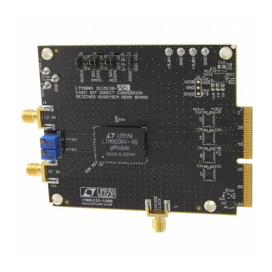
Demonstration circuit DC1513 is an evaluation board
featuring Linear Technology Corporation's LTM9004 14-
Bit Direct Conversion Receiver Subsystem. DC1513
demonstrates good circuit layout techniques and rec-
ommended external circuitry for optimal system per-
formance.
DC1513 comes with Linear Technology's 14-bit
LTM9004 receiver subsystem installed. The board in-
cludes output CMOS buffers. DC1513 plugs into the
DC890 Data Acquisition demo board and the output can
QUICK START PROCEDURE
Validating the performance of the LTM9004 is simple
with DC1513, and requires only two input sources, a
clock source, a computer, and a lab power supply. Refer
to Figure 1 for proper board evaluation equipment setup
and follow the procedure below:
1. Connect the power supply as shown in Figure 1.
There are on-board low-noise voltage regulators
that provide the two supply voltages for the
DC1513. The entire board and all components
share a common ground. The power supply should
still be a low-noise lab power supply capable of
supplying at least 0.5 Amp @ 5.0VDC, and 1 Amp
@ 3.0VDC.
2. Provide an encode clock to the ADC via SMA con-
nector J7. Use a low-phase-noise clock source
such as a filtered RF signal generator or a high-
quality clock oscillator.
NOTE. Similar to having a noisy input, a high-jitter (phase noise) encode
clock will degrade the signal-to-noise ratio (SNR) of the system.
DEMO CIRCUIT DC1513
LTM9004 14 Bit Direct
Conversion Receiver Subsystem
be easily analyzed with Linear Technology's PScope data
processing software, which is available for no charge on
our website at http://www.linear.com.
Design files for this circuit board are available. Call
the LTC factory.
L
, LTC, LTM, LT, Burst Mode, OPTI-LOOP, Over-The-Top and PolyPhase are registered
trademarks of Linear Technology Corporation. Adaptive Power, C-Load, DirectSense, Easy
Drive, FilterCAD, Hot Swap, LinearView, µModule, Micropower SwitcherCAD, Multimode
Dimming, No Latency ∆Σ, No Latency Delta-Sigma, No R
PowerPath, PowerSOT, SmartStart, SoftSpan, Stage Shedding, SwitcherCAD, ThinSOT,
UltraFast and VLDO are trademarks of Linear Technology Corporation. Other product names
may be trademarks of the companies that manufacture the products.
Table 1: DC1513 Connectors and Jumpers
REFERENCE
J3 (SHDN)
J4 (MODE)
J5 (SHDN_AMP)
J6 (LO)
J7 (CLK)
J8 (MIXER
ENABLE)
J11 (RF)
TP1 (SENSE_I)
TP2 (GND)
TP4 (GND)
TP5 (+3V)
TP7 (+5V)
TP8 (GND)
TP12 (SENSE_Q)
3. Apply an RF input signal to the board. For best
results, use a low distortion, low noise signal
QUICK START GUIDE
, Operational Filter, PanelProtect,
SENSE
FUNCTION
Enables/disables the ADC. Default is ON.
Output Format and Clock Duty Stabilizer pin.
Default is VDD.
Enables/disables the Amplifers. Default is ON.
Board LO Signal Input. Impedance-matched to
50Ω for use with lab signal generators.
Board Clock Input. Impedance-matched to
50Ω. Drive with a low-phase-noise clock oscil-
lator or filtered sine wave signal source.
Enables/disables the RF mixer. Default is ON.
Board RF Signal Input. Impedance-matched to
50Ω for use with lab signal generators.
Reference input to adjust the full-scale range of
the DC1513, I Channel. Default is VDD.
DC ground.
DC ground.
DC Supply input (3VDC).
DC Supply input (5VDC).
DC ground.
Reference input to adjust the full-scale range of
the DC1513, Q Channel. Default is VDD.
DC1513
1
Advertisement
Table of Contents

Related Manuals for Linear Technology DC1513


Summary of Contents for Linear Technology DC1513
- Page 1 LTM9004 receiver subsystem installed. The board in- PowerPath, PowerSOT, SmartStart, SoftSpan, Stage Shedding, SwitcherCAD, ThinSOT, UltraFast and VLDO are trademarks of Linear Technology Corporation. Other product names cludes output CMOS buffers. DC1513 plugs into the may be trademarks of the companies that manufacture the products.
- Page 2 DC890B, a USB cable, a Windows computer, and Linear Technology’s PScope data processing soft- 4. Apply an LO input signal to the board. Note that ware. the difference in frequency between this signal and the RF signal will be the IF frequency resulting at the IF filter and ADC input.
- Page 3 From the Configure menu in the toolbar, uncheck “Autodetect Device”. The default settings for DC1513 are shown in Figure 2. Figure 2. Entering the correct device information for your ADC. Select the correct parameters for the DC1513. Under normal conditions, PScope should automatically recognize the board and adjust the software settings accordingly.
- Page 4 DC1513 Figure 3. Schematic.
Need help?
Do you have a question about the DC1513 and is the answer not in the manual?
Questions and answers