Table of Contents
Advertisement
Quick Links
UM_2302_PL39_2304_090250
User manual for DEV_KIT_NGC1081
About this document
Scope and purpose
This document describes the evaluation kit for
field communication (NFC). The kit has all the necessary components to enable the user to quickly start sensing
the world via NFC in active and/or passive mode. The required settings for both modes, for programming and
debugging, are covered in this document.
Intended audience
This document aims to help developers make use of the NGC1081 in NFC sensing applications. It can also serve
as a demo for customers when used to sense different parameters at the same time.
Reference board/kit
Product(s) embedded on a PCB with a focus on specific applications and defined use cases that may include
software. PCB and auxiliary circuits are optimized for the requirements of the target application.
Note:
Boards do not necessarily meet safety, EMI and quality standards (for example UL, CE).
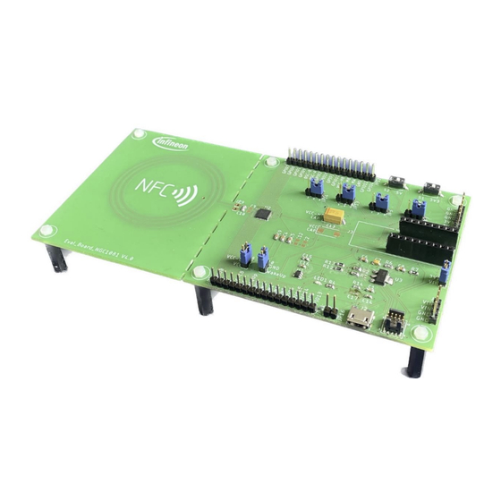
Figure 1
A photo of the Evaluation board EVAL_NGC1081
User manual
https://www.infineon.com/ngc1081
Infineon's NGC1081
Please read the sections "Important notice" and "Warnings" at the end of this
microcontroller, which supports near-
document
V 1.0
2023-04-12
Advertisement
Table of Contents

Related Manuals for Infineon NGC1081


Summary of Contents for Infineon NGC1081
-
Page 1: About This Document
Intended audience This document aims to help developers make use of the NGC1081 in NFC sensing applications. It can also serve as a demo for customers when used to sense different parameters at the same time. -
Page 2: Important Notice
Boards provided by Infineon Technologies. The design of the Evaluation Boards and Reference Boards has been tested by Infineon Technologies only as described in this document. The design is not qualified in terms of safety requirements, manufacturing and operation over the entire operating temperature range or lifetime. -
Page 3: Safety Precautions
User manual for DEV_KIT_NGC1081 Safety precautions Safety precautions Note: Please note the following warnings regarding the hazards associated with development systems. Table 1 Safety precautions Caution: A drive that is incorrectly applied or installed can lead to component damage or reduction in product lifetime. Wiring or application errors such as undersizing the motor, supplying an incorrect or inadequate AC supply, or excessive ambient temperatures may result in system malfunction. -
Page 4: Table Of Contents
User manual for DEV_KIT_NGC1081 Table of contents Table of contents About this document ........................1 Important notice ..........................2 Safety precautions .......................... 3 Table of contents ..........................4 The board at a glance ......................5 Scope of supply ............................5 Main features ............................ -
Page 5: The Board At A Glance
The board at a glance This development kit is a tool for engineers who want to use NGC1081 as a solution for sensing the world via NFC and energy harvesting. NGC1081 is an NFC tag-side controller, which combines in one device the functions of energy harvesting, NFC, sensing unit and motor control. - Page 6 Current between MA and MB I_HB Analog input AN_IN0 to AN_IN3 Analog outputs AN_OUT [*] The maximum external voltage should not exceed the selected clamping voltage of NGC1081 – see the datasheet for the possible values of the clamping voltage. User manual V 1.0...
-
Page 7: System And Functional Description
User manual for DEV_KIT_NGC1081 System and functional description System and functional description The EVAL_NGC1081 has been developed to operate in two different modes. It can operate either in active mode (by external wired power supply) or passive mode (by harvesting energy from the NFC antenna and without any external wired power supply). -
Page 8: Operation In Passive Mode
User manual for DEV_KIT_NGC1081 System and functional description Operation in passive mode In passive mode, the EVAL_NGC1081 not only communicates with the reader device (e.g., smartphone), but also harvests energy from it. 2.2.1 Steps to power up the board in passive mode Check jumper connections in Table •... -
Page 9: System Design
User manual for DEV_KIT_NGC1081 System design System design Schematics Figure 3 EVAL_ NGC1081 schematics User manual V 1.0 2023-04-12... -
Page 10: Layout
User manual for DEV_KIT_NGC1081 System design Layout Figure 4 EVAL_NGC1081 layout (top layer) Figure 5 EVAL_NGC1081 layout (bottom layer) User manual V 1.0 2023-04-12... -
Page 11: Bill Of Materials
EVAL_NGC1081 BOM Serial no. Part ref. Value Package Description MIC5365-3.3YD5-TR SOT95P280X100-5N LDO with 3.3 V output NGC1081 QFN32_NGC1081 Infineon tag-side microcontroller LDO with 2.5 V MIC5209-2.5YS SOT230P700X180-4N output 4, 5 C1, C16 100 nF C0603 Ceramic/X7R 6, 7, 8 C2, C3, C12... -
Page 12: Connector And Switch Details
(Recommended) connected when wake-up pin is not in JP11 NGC1081 pins (3) JP12 NGC1081 pins (4) JP13, JP14 UART and SPI connection between NGC1081 and S2GO JP15 5 V pinouts connected to the S2GO sensors Debugger connector Micro-USB connector S2GO sensors connector... -
Page 13: System In Operation
System in operation System in operation To sense the world using NGC1081, you can use the internal temperature sensor or any of the other peripherals C, SPI, UART ...) that the NGC1081 supports to sense using external sensors. For an easy trial of different sensors, the EVAL_NGC1081 supports the S2GO boards. -
Page 14: Steps To Measure Co
(available in active and/or in passive mode). After going through one of the two options, the NGC1081 sends the results over UART. The results can be read using the Android app supplied with the board. Below is the flow chart of the firmware. - Page 15 User manual for DEV_KIT_NGC1081 System in operation Figure 10 measurement steps labeled on the EVAL_NGC1081 with the SHIELD_PASCO2_SENSOR After less than 2 s the result will already be shown on the UART terminal. 6. Additionally, if the phone is placed where the NFC antenna is, the result of the measurement will also be shown in the app.
-
Page 16: Steps To Measure Temperature
1. Plug the micro-USB into J2 for power supply. 2. Make sure the following jumper is connected correctly: a. JP8 connected 3. Connect the Rx UART cable to GPIO2 (Tx of the NGC1081). 4. Switch S1 on. Figure 13 shows the steps mentioned above on the board. -
Page 17: Passive Mode Temperature Measurement
User manual for DEV_KIT_NGC1081 System in operation The figures below show the results of temperature measurements. Figure 14 Screenshot of the result on the app terminal after temperature measurement Figure 15 Screenshot of the result on the UART terminal after temperature measurement 4.2.2.2 Passive mode temperature measurement For passive mode temperature measurement, there are just two steps:... -
Page 18: Appendices
Appendices Appendices Debugger connection NGC1081 IC supports Arm® SWD and TAG debug ports for firmware programming. Figure 16 shows the connection of the debugger to the device. Two signals of the SWD debug port – SWDCLK and SWDIO – are connected with the pull-down resistors of 100 kΩ. -
Page 19: Bnfc Antenna
The evaluation kit offers an antenna as part of the evaluation board. An additional finished antenna design can be downloaded from the NGC1081 product web page. It is also possible to remove the antenna on the PCB and use an external antenna by connecting it to JP9. NFC readers operate in the 13.56 MHz high-frequency band. -
Page 20: Glossary
User manual for DEV_KIT_NGC1081 Glossary Glossary S2GO Shield 2GO EVAL_NGC1081 Evaluation board NGC1081 User manual V 1.0 2023-04-12... -
Page 21: Revision History
User manual for DEV_KIT_NGC1081 Revision history Revision history Document Date Description of changes revision V 1.0 2023-04-12 Initial release User manual V 1.0 2023-04-12... -
Page 22: Disclaimer
For information on the types in question please contact your nearest Published by Infineon Technologies office. Infineon Technologies AG Except as otherwise explicitly approved by Infineon 81726 Munich, Germany Technologies in a written document signed by authorized representatives Infineon Technologies, Infineon Technologies’...
Need help?
Do you have a question about the NGC1081 and is the answer not in the manual?
Questions and answers