Table of Contents
Advertisement
Quick Links
GS-EVB-HBDB-IMS
650 V Universal Half Bridge Isolated Driver Motherboard for IMS2
& IMS3
Technical Manual
____________________________________________________________________________________________________________________________________________
GS-EVB-HBDB-IMS
650 V Universal Half Bridge Isolated Driver Motherboard for IMS2
& IMS3
Technical Manual
Visit
www.gansystems.com
for the latest version of this technical manual.
GS-EVB-HBDB-IMS TM Rev. 220329
© 2022 GaN Systems Inc.
www.gansystems.com
1
Please refer to the Evaluation Board/Kit Important Notice on page 19
Advertisement
Table of Contents

Related Manuals for Gan Systems GS-EVB-HBDB-IMS


Summary of Contents for Gan Systems GS-EVB-HBDB-IMS
- Page 1 650 V Universal Half Bridge Isolated Driver Motherboard for IMS2 & IMS3 Technical Manual Visit www.gansystems.com for the latest version of this technical manual. GS-EVB-HBDB-IMS TM Rev. 220329 © 2022 GaN Systems Inc. www.gansystems.com Please refer to the Evaluation Board/Kit Important Notice on page 19...
- Page 2 This product contains parts that are susceptible to damage by electrostatic discharge (ESD). Always follow ESD prevention procedures when handling the product. GS-EVB-HBDB-IMS TM Rev. 220329 © 2022 GaN Systems Inc. www.gansystems.com Please refer to the Evaluation Board/Kit Important Notice on page 19...
-
Page 3: Table Of Contents
DC Link Decoupling Capacitors ......................9 IMS Half Bridge Daughter Power Board Options ..................10 Test Results ................................ 12 Double Pulse Test (GS-EVB-HBDB-IMS + GS-EVB-IMS3-66508B-GS) ..........12 Boost Configuration Test (GS-EVB-HBDB-IMS + GS-EVB-IMS3-66508B-GS) ........ 14 GS-EVB-HBDB-IMS Schematics and BoM ....................16 GS-EVB-HBDB-IMS TM Rev. - Page 4 Figure 19 Test waveforms (400Vin, 10kHz, Po=0.8kW) ..................15 List of Tables Table 1 GS-EVB-IMS3-665xxB-GS Evaluation Kit Contents ................. 5 Table 2 Compatible IMS daughter power board for driver motherboard GS-EVB-HBDB-IMS ....10 Table 3 Part numbers and description ........................12 GS-EVB-HBDB-IMS TM Rev. 220329 ©...
-
Page 5: Overview
1 Overview 1.1 Introduction GS-EVB-HBDB-IMS is a 650 V universal half-bridge motherboard with 2 isolated gate drivers. The daughter power boards that are compatible with this driver motherboard are available in 2 power levels: 3kW and 6kW. This document mainly focuses on introducing the design and application of the driver motherboard. -
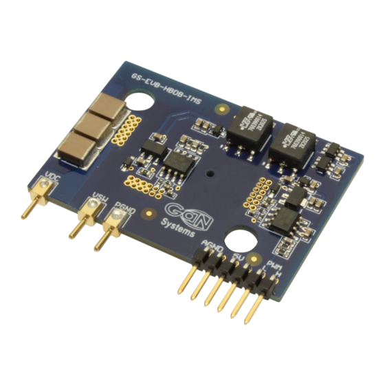
Page 6: Figure 1 Ims Evb Motherboard Gs-Evb-Hbdb-Ims
GS-EVB-HBDB-IMS 650 V Universal Half Bridge Isolated Driver Motherboard for IMS2 & IMS3 Technical Manual ____________________________________________________________________________________________________________________________________________ Figure 1 IMS EVB motherboard GS-EVB-HBDB-IMS Figure 2 Assembled IMS EVB module with heatsink GS-EVB-HBDB-IMS TM Rev. 220329 © 2022 GaN Systems Inc. www.gansystems.com... -
Page 7: Motherboard Technical Specifications
Figure 3 Circuit block diagram of IMS EVB Module Figure 4 Labelled driver motherboard GS-EVB-HBDB-IMS TM Rev. 220329 © 2022 GaN Systems Inc. www.gansystems.com Please refer to the Evaluation Board/Kit Important Notice on page 19... -
Page 8: Gate Driver Circuit
R2 and R3 are gate turn-on and off resistors. 2.3 5V Input and External PWM Signals Input Figure 6 External 5V and PWM signals connector pin GS-EVB-HBDB-IMS TM Rev. 220329 © 2022 GaN Systems Inc. www.gansystems.com Please refer to the Evaluation Board/Kit Important Notice on page 19... -
Page 9: Temperature Monitoring Hole
As it is challenging to create a low inductance power loop on a single-layer IMS board, DC decoupling capacitors are placed on a multi-layer IMS EVB PCB. The power loop path is highlighted below. GS-EVB-HBDB-IMS TM Rev. 220329 © 2022 GaN Systems Inc. -
Page 10: Ims Half Bridge Daughter Power Board Options
(3 kW) and high power (6 kW), normal thermal conductivity (3K) and high thermal conductivity (7K). The ordering options are listed in table 2: Table 2 Compatible IMS daughter power boards for driver motherboard GS-EVB-HBDB-IMS IMS2 and IMS3 HALF BRIDGE DAUGHTER... -
Page 11: Figure 10 Compatible Ims3 Daughter Power Boards
(K factor) of the dielectric layer of the IMS board. Figure 12 Cross-section view of a single layer IMS board Using this platform power designers can evaluate the electrical and thermal performance of GaN Systems’ E-mode transistor in high power, high-efficiency applications. The ordering information are listed below: GS-EVB-HBDB-IMS TM Rev. -
Page 12: Test Results
Evaluate the GaN E-mode performance in any half-bridge based topology, over a range of operating conditions. This can be done using either the accompanying power motherboard (P/N: GS-EVB-HBDB-IMS) or with the users’ own board for in-system prototyping. • Use as a thermal and electrical design reference of the GS66516B or GS66508B GaN ®... -
Page 13: Figure 14 Double Pulse Test Setup
650 V Universal Half Bridge Isolated Driver Motherboard for IMS2 & IMS3 Technical Manual ____________________________________________________________________________________________________________________________________________ Figure 14 Double pulse test setup Figure 15 Double pulse test waveforms (400V/30A) GS-EVB-HBDB-IMS TM Rev. 220329 © 2022 GaN Systems Inc. www.gansystems.com Please refer to the Evaluation Board/Kit Important Notice on page 19... -
Page 14: Boost Configuration Test (Gs-Evb-Hbdb-Ims + Gs-Evb-Ims3-66508B-Gs)
GS-EVB-HBDB-IMS 650 V Universal Half Bridge Isolated Driver Motherboard for IMS2 & IMS3 Technical Manual ____________________________________________________________________________________________________________________________________________ 4.2 Boost Configuration Test (GS-EVB-HBDB-IMS + GS-EVB-IMS3-66508B-GS) • Test condition: V = 400V, f =10kHz, Po=0.8kW, T = 25℃. • Device case temperature 72℃... -
Page 15: Figure 18 Boost Configuration Test Thermal Measurement Result
Figure 18 Boost configuration test thermal measurement result Figure 19 Test waveforms (400Vin, 10kHz, Po=0.8kW) Ch#1 (blue): Drain-source voltage, 100V/div Ch#4 (green): Inductor current, 5A/div GS-EVB-HBDB-IMS TM Rev. 220329 © 2022 GaN Systems Inc. www.gansystems.com Please refer to the Evaluation Board/Kit Important Notice on page 19... -
Page 16: Gs-Evb-Hbdb-Ims Schematics And Bom
GS-EVB-HBDB-IMS 650 V Universal Half Bridge Isolated Driver Motherboard for IMS2 & IMS3 Technical Manual ____________________________________________________________________________________________________________________________________________ 5 GS-EVB-HBDB-IMS Schematics and BoM GS-EVB-HBDB-IMS motherboard schematics GS-EVB-HBDB-IMS TM Rev. 220329 © 2022 GaN Systems Inc. www.gansystems.com Please refer to the Evaluation Board/Kit Important Notice on page 19... - Page 17 GS-EVB-HBDB-IMS 650 V Universal Half Bridge Isolated Driver Motherboard for IMS2 & IMS3 Technical Manual ____________________________________________________________________________________________________________________________________________ GS-EVB-HBDB-IMS assembly drawing (top layer) Mid Layer 1 Top Layer Mid Layer 2 Bottom Layer GS-EVB-HBDB-IMS PCB layout (4-layer PCB) GS-EVB-HBDB-IMS TM Rev. 220329 ©...
- Page 18 GS-EVB-HBDB-IMS 650 V Universal Half Bridge Isolated Driver Motherboard for IMS2 & IMS3 Technical Manual ____________________________________________________________________________________________________________________________________________ GS-EVB-HBDB-IMS Bill of Materials (BOM) Designator Description Quantity Manufacturer Manufacturer Part Number C1, C9, C16, Samsung Electro- CAP CER 4.7UF 10V X5R 0402 Mechanics...
- Page 19 The user assumes all responsibility and liability for proper and safe handling of the goods. Further, the user indemnifies GaN Systems from all claims arising from the handling or use of the goods. Due to the open construction of the product, it is the user’s responsibility to take any and all appropriate precautions with regard to electrostatic discharge.
- Page 20 The information given in this document shall not in any event be regarded as a guarantee of performance. GaN Systems hereby disclaims any or all warranties and liabilities of any kind, including but not limited to warranties of non-infringement of intellectual property rights.
Need help?
Do you have a question about the GS-EVB-HBDB-IMS and is the answer not in the manual?
Questions and answers